HAL Id: hal-00273766
https://hal.archives-ouvertes.fr/hal-00273766
Submitted on 16 Apr 2008
HAL is a multi-disciplinary open access
archive for the deposit and dissemination of
sci-entific research documents, whether they are
pub-lished or not. The documents may come from
teaching and research institutions in France or
abroad, or from public or private research centers.
L’archive ouverte pluridisciplinaire HAL, est
destinée au dépôt et à la diffusion de documents
scientifiques de niveau recherche, publiés ou non,
émanant des établissements d’enseignement et de
recherche français ou étrangers, des laboratoires
publics ou privés.
Through-silicon via based 3D IC technology:
Electrostatic simulations for design methodology
Maxime Rousseau, Olivier Rozeau, Gérald Cibrario, Gilles Le Carval,
Marie-Anne Jaud, Patrick Leduc, Alexis Farcy, Antoine Marty
To cite this version:
Maxime Rousseau, Olivier Rozeau, Gérald Cibrario, Gilles Le Carval, Marie-Anne Jaud, et al..
Through-silicon via based 3D IC technology: Electrostatic simulations for design methodology.
IMAPS Device Packaging Conference, Mar 2008, Phoenix, AZ, United States. pp.Session WA1:
wafer-level 3D integration and through-silicon vias (TSVs) - II. �hal-00273766�
Through-silicon via based 3D IC technology:
Electrostatic simulations for design methodology
M. Rousseau1,3, O. Rozeau2, G. Cibrario2, G. Le Carval2, M.-A. Jaud2, P. Leduc2,A. Farcy1, A. Marty3
1
STMicroelectronics - 850, rue Jean Monnet - 38926 Crolles cedex - France
2
CEA-LETI/MINATEC - 17, rue des Martyrs - 38054 Grenoble cedex 9 - France
3
LAAS-CNRS, Université de Toulouse - 7, avenue du Colonel Roche - 31077 Toulouse cedex 4 - France Corresponding author: [email protected], tel.: +33438780635, fax: +33438785012 Keywords: through silicon via, 3D integration, parasitic coupling, electrostatic compatibility, design methodology, layout.
Abstract
Two parallel methods of simulation have been developed in order to evaluate the electrostatic impact that a through-silicon via (TSV) may have on a 65 nm MOS transistor. The first model is based on the finite element method (FEM) and the second one is related to electric component models (SPICE language). Both approaches are then compared and discussed. The SPICE model has been calibrated on the numerical one, so that it can be used for more complex devices – here, an inverter – and more systematic investigations. A range of 3D-compatible design rules have been defined. By integrating these new data on a complete 3D design methodology, we are able to design and layout simple logic circuitries based on a 2-stratum 3D architecture.
Introduction
As 2-dimensional IC scaling becomes more and more difficult to achieve for the next technological nodes, 3D IC technology is being considered as a real breakthrough approach. It seems to be an interesting solution in terms of IC design and manufacturing [1,2]. 3D integration doubtlessly brings significant benefits concerning circuit performance, density of integration, interconnect power consumption and heterogeneous technology integration capabilities [3]. Microelectronics worldwide actors tend to develop a through-silicon via technology (TSV) in order to connect stacked ICs to each others. TSV appears to be one of the greatest technology challenges brought by 3D integration. As TSV can be considered as a brand new entity in conventional IC architectures, electrical parasitic coupling and critical substrate noise might occur in neighboring active devices. These electrostatic phenomena have to be taken into account to ensure reliable circuit design [4]. Quantifying such effects allows designers to fit 2D design rules to 3D requirements. Another serious issue about 3D technology is that current design tools do not include 3D layout possibilities yet. Beyond TSV considerations, all the conventional design procedures and layout capabilities are unsuitable for 3D integration. At that time, only few labs or companies had developed 3D-compatible design methodologies that could lead to an electrical demonstration [2,5,6,7], but they are not commercially available. Allowing 3D design for the current 2D tools will fully release all the powerful capabilities of vertical architecture.
Copper TSV based 3D integration
There are many possibilities to integrate vertically two (or more) active strata, depending on the application-driven choice and the available 3D process steps. Bonding techniques (molecular, BCB, metal, etc), upper wafer orientations (face-to-face or back-to-face), remaining silicon thickness, alignment techniques are as many parameters that will impact design.
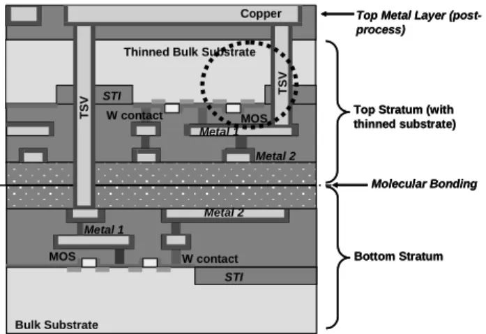
In this paper, we focus on a two-stratum integration flow developed at the CEA/Léti, using molecular bonding [8,9] that can be achieved either by wafer-to-wafer or die-to-wafer techniques. The two active bulk strata are face-to-face oriented. Top stratum backside silicon is thinned down to about 10 µm. Two kinds of through-silicon vias are integrated: one to connect the top metal layer to the metal 1 of top stratum, and another one to connect the top metal layer to the last metal level of bottom stratum (Figure 1). TSV are etched, isolated with oxide and filled with copper. TSV dimensions are typically 2-3 µm wide and 10-12 µm deep. The top metal layer is then deposited over the backside thin silicon layer in order to interconnect TSV to each other. Top metal layer dimensions are relaxed compared to the other metal lines because I/Os are also designed at the same physical level. I/Os involve wide metal lines to enable distribution of power, clock signals and ESD protections.
MOS W contact
Thinned Bulk Substrate
STI
Metal 1 Metal 2
Top Stratum (with thinned substrate) Molecular Bonding MOS W contact STI Metal 1 Metal 2 Bulk Substrate Bottom Stratum T S V T S V
Copper Top Metal Layer (post-process)
MOS W contact
Thinned Bulk Substrate
STI
Metal 1 Metal 2
Top Stratum (with thinned substrate) Molecular Bonding MOS W contact STI Metal 1 Metal 2 Bulk Substrate Bottom Stratum T S V T S V Copper
Copper Top Metal Layer (post-process)
Figure 1. Copper TSV-based bulk face-to-face integration, using molecular bonding.
2D FEM modeling of TSV-induced electrostatic impact on device performances
In all 3D integration schemes, only the top stratum is clearly exposed to the electrostatic disturbances that may be produced by TSV. Indeed, bottom stratum devices are protected by the fact that TSV are connected to the last metal level of the interconnect network, far from the active area. Top stratum devices could be surrounded by several TSV that all pass through the thinned silicon substrate. This study is focused on TSV-CMOS local area depicted on Figure 1 (dotted line), and works with any 3D integration scheme.
In order to quantify parasitic coupling within the thinned silicon substrate, a simple structure is numerically meshed, using the finite elements method. The 2D TCAD software used is Silvaco Atlas [10]. A single 65 nm-based, low power MOS transistor implemented in the thinned silicon substrate and located near a TSV is considered. The whole structure is depicted on Figure 2 – left (dimensions are not scaled). The electrical behavior of the MOS transistor is simulated by the SIMS-based doping profile of 65 nm CMOS technology. As TSV dimensions are much bigger than the MOS ones, meshing the entire TSV is difficult because of the limited number of meshing nodes. So, TSV is considered as a perfect conductor and is represented on the structure as an electrode applied on the whole left vertical limit of the meshing.
To validate the FEM-based model, MOS electrical behavior has been calibrated on the 65 nm electrical models (Design Kit). It is shown that the (Ion/Ioff) ratio from TCAD is 1.2 time higher than the one from the design kit
model. TCAD-based threshold voltage VT is equal to 0.41 V, i.e. 0.1 V lower than the design kit-based VT. The
MOS electrical behavior obtained by FEM-based simulation is very close to its design kit-based model.
The MOS transistor is plugged on its static mode (Vg = Vd = 1.2 V). A square voltage VTSV (f = 200 MHz, 200
ps-long rising and falling ramp times, 3.3 V peak voltage) is then applied on the TSV. A local body potential VB, located in between the channel at 0.5 µm under the oxide-silicon interface, is extracted during a transient
analysis. This position enables to quantify the finest electrical disturbances that may modify the electrical behavior of carriers in the channel. We observed that body potential peaks occur at each rising and falling VTSV
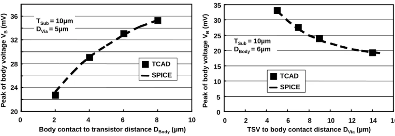
ramp (Figure 2 – right). Distances between body contact and TSV (Dvia), body contact and MOS (Dbody) and
substrate thickness (Tsub) were parameterized to evaluate the direct influence of the structure geometry on
substrate noise. Maximal values of VB were extracted when decreasing Dvia value and increasing Dbody and Tsub
values (as shown on Figure 3). From that, Tsub is set to 10µm, which is a feasible technological requirement.
STI Oxide T S V i s o la ti o n
Thin silicon substrate
Body contact (GND) TSV STI Oxide Oxide STI Oxide S-D contacts VT S V VB
Highly doped layer
Gate Drain Source Dvia Dbody Ts u b -3.5 -2.5 -1.5 -0.5 0.5 1.5 2.5 3.5 0 2 4 6 8 10 12 14 16 Time (ns) T S V v o lt a g e V T S V ( V ) -0.03 -0.02 -0.01 0 0.01 0.02 0.03 B o d y V o lt a g e V B ( V ) -3.5 -2.5 -1.5 -0.5 0.5 1.5 2.5 3.5 0 2 4 6 8 10 12 14 16 Time (ns) T S V v o lt a g e V T S V ( V ) -0.03 -0.02 -0.01 0 0.01 0.02 0.03 B o d y V o lt a g e V B ( V )
2D SPICE modeling of CMOS devices within a 3D integration
The previous numerical simulation allows the extraction of physics-based results. Nevertheless, the cost of simulation time is expensive. One solution is to employ SPICE-like simulation using a circuit simulator (Eldo) in which the results are quasi instantaneous. For this reason, the previous structure was adapted to simulate the impact of the TSV with circuit simulator. The silicon substrate model is composed of 3400 resistors approximately with a grid defined by ∆x=0.5µm (horizontal) and ∆y=TSub/20 (vertical). The barrier oxide is
modeled by a set of MOS capacitances. Finally, the MOS transistor is modeled using BSIM4.
To compare numerical simulation with circuit simulation, a set of numerical simulations was performed using a n-channel transistor with channel length and width L=W=1µm. The substrate thickness value is 10µm.
Figure 3 compares both approaches where the peak of body voltage (from Figure 2 - right) is plotted as a function of body contact-to-transistor distance (Dbody) and TSV-to-body contact distance (Dvia). Note that
substrate and highly doped layer resistivities are adjusted for SPICE simulation to fit perfectly with the numerical simulations.
These last figures validate the SPICE-like approach for a wide range of distances. In the next part, this approach will be used to estimate the influence of the TSV on circuit performances for digital and analog applications.
20 24 28 32 36 0 2 4 6 8 10 TSub= 10µm DVia= 5µm P e a k o f b o d y v o lt a g e VB (m V )
Body contact to transistor distance DBody(µm) TCAD SPICE 0 5 10 15 20 25 30 35 0 2 4 6 8 10 12 14 16 TSub= 10µm DBody= 6µm TCAD SPICE P e a k o f b o d y v o lt a g e V B (m V )
TSV to body contact distance DVia(µm)
Figure 3. Comparison between TCAD and SPICE simulations: peak of body voltage VB versus body
contact-to-transistor distance DBody (Left) and versus TSV-to-body contact distance DVia (Right).
Estimation of the impact of TSV on circuit performances
The aim of this section is to evaluate the impact of the TSV on the circuit operations. To achieve it, basic simulations were performed using the SPICE-based model. On one hand, we propose to study TSV impact on the inverter in transient simulation for digital applications. On the other hand, the impact of coupling between the TSV and the transistor in AC and noise simulations is investigated for analog applications. These textbook cases could be used to define new design rules to preserve circuit performances.
Digital applications
This part is based on the investigation of inverter behavior in transient simulation. This inverter is designed with a 2D approach, as illustrated on Figure 4. pMOSFET is realized in n-doped region. Compared to nMOSFET, the p-channel transistor is less sensitive to fluctuations of substrate potential. In order to simplify the study, a coupling only between the TSV and the nMOSFET body voltage is supposed.
Device geometries are W/L=120nm/65nm and W/L=240nm/65nm for n and pMOSFET, respectively. Square signals are applied on the TSV, noted VTSV, and on the input of inverter, noted VIN, at 200MHz and 72MHz
frequencies respectively. A capacitance load of 200 fF is plugged at the inverter output.
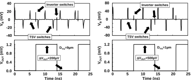
Figure 5 shows the results of the transient simulation on two configurations DVia=1µm and 9µm. Spikes on the
nMOS body voltage appear during the rising and falling ramp times of TSV and input voltages. Nevertheless, the output voltage is not affected by the commutation of TSV voltage. The output voltage dispersion due to the TSV switching is estimated lower than 500 µV for the worst case. From these results, it seems that the TSV has quite no influence on digital circuit behavior. In addition, these results obtained using a 2D approach are probably pessimistic compared to a 3D simulation where body control with the body contacts will be more efficient. As a conclusion, specific design rules are not necessary for this type of application. Design rules will be only defined from technological and process points of view (mask alignment for example).
STI oxide STI oxide STI oxide STI oxide
Thin silicon substrate
nMOSFET pMOSFET T S V i s o la ti o n Dbody GND TSV VDD Dvia IN IN OUT
Highly doped layer
Figure 4. Schematic cross section of inverter.
0.0 0.4 0.8 1.2 0 5 10 15 20 25 -40 -20 0 20 40 VO U T (m V ) Time (ns) VB (m V ) TSV switches Inverter switches DVia=9µm ∆∆∆∆VOUT<200µV 0 5 10 15 20 25 Time (ns) 0.0 0.4 0.8 1.2 -80 -40 0 40 80 VO U T (m V ) VB (m V ) TSV switches Inverter switches DVia=1µm ∆∆∆∆VOUT<500µV
Figure 5. Transient simulation of inverter with DBody=5.0µm and (Left) DVia=9µm and (Right) DVia=1µm.
Analog applications
The aim of this paragraph is to highlight the parasitic coupling between the transistor and the TSV.
A small signal voltage source dVTSV is applied on the TSV. The isolation dVB/dVTSV is calculated from AC
simulation. The transistor is a nMOSFET with L=65nm and W=1µm. This coupling is a high-pass filter due to the TSV insulator as shown on Figure 6 (Left) where dVB/dVTSV, noted H, is calculated versus frequency. On
this figure, Hmin is the minimum of the isolation and fC is its cut-off frequency.
-300 -200 -100 0 100k 1M 10M 100M 1G 10G 100G H = d vB /d vT S V (d B ) GND Rb VB Rs diD Cb GND Rb VB Rs diD Cb dvTSV FC@ Hmin-3dB Hmin Frequency (Hz) DBody=2µm DVia=1-5-10-15µm -21 -20 -19 -18 0 0.1 0.2 0.3 0.4 0.5 0.6 0.7
Oxide isolation thickness (µm) Hm in (d B ) 0 2 4 6 8 10 12 fC (G H z ) DVia= 1µm DBody= 2µm
Figure 6. (Left) Transfer function dVB / dVTSV versus frequency and (Right) figures-of-merit versus oxide
For low frequency applications, the electrostatic coupling between the TSV and the body is pretty weak. It becomes significant for frequencies higher than 100 MHz. Increasing the distance between TSV and body contact affects the coupling at high frequency but can be insufficient for a low noise amplifier.
For better isolation, an obvious solution is to increase the barrier oxide thickness during the process. However, as illustrated on Figure 6 (Right), this technological parameter has a low impact on Hmin. Only the cut-off frequency
fC is affected by the barrier oxide thickness. This solution is not efficient for robust design.
For analog applications, the impact of the TSV depends on the frequency operation and the noise figure needs. For example, in the case of high-gain amplifier, the TSV could inject noise into amplifier chain. A solution consists in guarding the TSV using another TSV connected to the ground. This solution will be probably more efficient than a guard ring using body contact (less deep). Nevertheless, for general case in analog applications, the impact of TSV must be annihilated by using a guard ring.
3D upgrade of design environment using standard tools
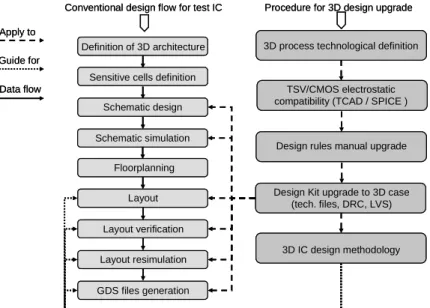
As there is no commercial 3D-suitable design environment yet, designing 3D test circuitries first appears hazardous. Very few research teams are working to achieve a 3D standard-cell place and route tool and a 3D circuit layout editor [7,11]. The primary goal consists in upgrading the 65 nm advanced technology design kit to allow simple 3D sensitive cells design. Place & Route automation is not allowed here. This procedure works only for simple logic circuits on two active strata, with few gates that should be placed and routed by hand. To achieve 3D design upgrade, the new design rules previously defined are included in the 65nm CMOS technology DRM and a new layout methodology is implemented. This work is carried out with Cadence design environment. The proposed approach is depicted on Figure 7.
The layout sequence can be split up in four steps:
1. Layout generation of bottom tier: create the whole bottom layout with TSV layers.
2. “Mirror view” generation of bottom tier layout: allow to flip the bottom tier layout and create a mirror view of the TSV passing through top stratum.
3. Layout generation of flipped top tier: create the top tier layout by taking into account the TSV locations coming from the bottom tier according to the bottom layout mirror view.
4. Final layout generation: allow to layout the top metal interconnections between TSV and I/O.
Simple logic circuits designed for test can be achieved using this layout methodology with Cadence design environment.
Design Kit upgrade to 3D case (tech. files, DRC, LVS) Definition of 3D architecture
Sensitive cells definition Schematic design Floorplanning Layout Layout verification Layout resimulation GDS files generation TSV/CMOS electrostatic compatibility (TCAD / SPICE ) Apply to
Guide for Data flow
3D process technological definition Conventional design flow for test IC Procedure for 3D design upgrade
Schematic simulation
3D IC design methodology Design rules manual upgrade
Conclusion
3D integration is considered as a breakthrough technology with a promising potential. Moreover, 3D integration can be adapted to a large field of applications. Up to now, TSV technology development and 3D IC design are the two main challenges of 3D integration. We showed that TSV have a certain electrostatic impact on advanced technology devices. From this statement, parasitic effects could be decreased if TSV-CMOS spatial configurations are optimized. A SPICE-based model calibrated on a FEM-based numerical model has been developed. This easy-to-use model allowed to estimate TSV impact on circuit performances both in analog and digital applications. As a result, no specific design rules are necessary for digital operating mode. Nevertheless, TSV operation involves parasitic coupling for frequencies higher than 100 MHz in analog mode. In this case, specific design rules have been defined in order to ensure a reliable electrical compatibility. These new design rules defined both from the coupling study and technological requirements allowed to update the 65 nm technology design kit. A 3D-dedicated layout methodology has been implemented. Even if our design flow is place-and-route limited, it allows manufacturing of 3D sensitive cells for test. From now on, a real in-depth revision of current design environments will ensure 3D-based architectures to become a relief to interconnect-driven IC design [1,2,11].
Acknowledgements
This work was carried out in the frame of CEA-LETI/MINATEC and STMicroelectronics collaboration. The authors would like to thank Marc Belleville of LETI’s Design Department for his advice.
References
[1] K. Banerjee et al., 3D ICs : a novel chip design for improving deep-submicrometer interconnect performance and Systems-on-Chip integration, Proceedings of the IEEE, vol. 89, No. 5, May 2001.
[2] W.R. Davis et al., Demystifying 3D ICs: The pros and cons of going vertical, IEEE Design & Test of Computers, 2005, pp 498-510.
[3] S.J. Souri et al., Multiple Si layer ICs: motivation, performance analysis and design implications, 37th Conference on Design Automation (DAC'00), 2000, pp 213-220.
[4] G. Elst, Modeling and simulation of parasitic effects in stacked silicon, MRS Symposium Proceedings, Vol. 970, 2007.
[5] P.R. Morrow et al., Three-dimensional wafer stacking via Cu-Cu bonding integrated with 65-nm strained-Si/Low-k CMOS technology, IEEE electron device letters, vol. 27, No. 5, May 2006, pp 335-337.
[6] P. Jacob et al., Predicting the performance of a 3D processor-memory chip stack, IEEE Design & Test of Computers, 2005, pp. 540-547.
[7] S.M. Alam et al., A comprehensive layout methodology and layout-specific circuit analyses for three-dimensional integrated circuits, ISQED 2002 Proceedings.
[8] R. Chatterjee et al., Three dimensional chip stacking using a wafer-to-wafer integration, IITC 2007 Proceedings.
[9] P. Leduc et al., Enabling technologies for 3D chip stacking, VLSI-TSA 2008 Proceedings. [10] Silvaco International, Atlas User’s Manual, www.silvaco.com