HAL Id: hal-02955765
https://hal.archives-ouvertes.fr/hal-02955765
Submitted on 5 Oct 2020HAL is a multi-disciplinary open access archive for the deposit and dissemination of sci-entific research documents, whether they are pub-lished or not. The documents may come from teaching and research institutions in France or abroad, or from public or private research centers.
L’archive ouverte pluridisciplinaire HAL, est destinée au dépôt et à la diffusion de documents scientifiques de niveau recherche, publiés ou non, émanant des établissements d’enseignement et de recherche français ou étrangers, des laboratoires publics ou privés.
Recent measurements on MiniMALTA, a radiation hard
CMOS sensor with small collection electrodes for
ATLAS
Patrick Moriishi Freeman, P. Allport, I. Asensi Tortajada, M. Barbero, S.
Bhat, D. Bortoletto, I. Berdalovic, C. Bespin, C. Buttar, I. Caicedo, et al.
To cite this version:
Patrick Moriishi Freeman, P. Allport, I. Asensi Tortajada, M. Barbero, S. Bhat, et al.. Recent measurements on MiniMALTA, a radiation hard CMOS sensor with small collection electrodes for ATLAS. 28th International Workshop on Vertex Detectors, Oct 2019, Lopud Island, Croatia. pp.020, �10.22323/1.373.0020�. �hal-02955765�
Recent measurements on MiniMALTA, a radiation
hard CMOS sensor with small collection electrodes
for ATLAS
P. M. Freeman∗
The University of Birmingham (UK), CERN
E-mail:[email protected]
P. Allporta, A. Andreazzap,I. Asensi Tortajadab,c, M. Barberom, S. Bhatm, D.
Bortolettod, I. Berdalovicb, j, C. Bespink, C. Buttarg, I. Caicedok, R. Cardellab,e, F.
Dachsb, f, V. Daob, Y. Degerlin, H. Denizlil, M. Dyndalb, L. Flores Sanz de Acedob,g, L.
Gonellaa, A. Habibm, T. Hemperekk, T. Hironok, T. Kugathasanb, V. Liberalip, I.
Mandi ´ch, D. Maneuskig, K. Metodievd, M. Mikužh, M. Mironovad, K. Moustakask, M.
Munkerb, K. Y. Oyulmazl, P. Pangaudm, H. Perneggerb, F. Pirob, R. Plackett, P.
Riedlerb, H. Sandakere, E. J. Schioppaa, P. Schwemlingn, A. Sharmab,d, I. Shipseyd,
L. Simon Argemimg, C. Solans Sanchezb, W. Snoeysb, T. Suligojj, L. Vigorellip, T.
Wangk, D. Weatherilld, H. Wennlöfa, N. Wermesk , D. Woodd, S. Worma,o
aUniversity of Birmingham, Birmingham, United Kingdom,bCERN,cUniversity of Valencia and
Consejo Superior de Investigaci Científicas (CSIC), Valencia, Spain ,dUniversity of Oxford, Oxford, United Kingdom,eUniversity of Oslo, Oslo, Norway ,fVienna University of Technology, Vienna, Austria ,gUniversity of Glasgow, Glasgow, United Kingdom ,iJožef Stefan Institute, Ljubljana, Slovenia , jUniversity of Zagreb, Zagreb, Croatia ,kRheinische Friedrich-Wilhelms
Universität Bonn, Bonn, Germany ,lBolu Abant Izzet Baysal University, Bolu, Turkey ,mAix Marseille University, CNRS/IN2P3, CPPM, Marseille, France ,nCEA-IRFU, Paris, France ,
PoS(Vertex2019)020
The upgrade of the ATLAS tracking detector for the High-Luminosity Large Hadron Collider at CERN requires the development of novel radiation hard silicon sensor technologies.
The MALTA Monolithic Active Pixel Sensor prototypes have been developed with the 180 nm TowerJazz CMOS imaging technology. This combines the engineering of high-resistivity sub-strates with on-chip high-voltage biasing to achieve a large depleted active sensor volumes, to meet the radiation hardness requirements of the outer barrel layers of the ATLAS ITK Pixel
de-tector (1.5× 10151 MeV n
eq/cm2and 80 MRad TID). MALTA combines low noise (ENC < 20
e−) and low power operation (1 uW / pixel) with a fast signal response (25 ns bunch crossing) in
small pixel size (36.4 × 36.4 µm2), and a small collection electrode (3 µm), with a novel
high-speed asynchronous read out architecture to cope with the high hit rates expected at HL-LHC. The latest developments, embedded in so-called Mini-MALTA chip, address the issues observed in previous designs to meet the desired radiation hardness requirements. This contribution will summarize the design and recent improvements of this technology, together with the measure-ments of analog and digital performance, as obtained in test beams and lab and radioactive source tests.
The 28th International Workshop on Vertex Detectors - Vertex2019 13-18 October, 2019
Lopud, Croatia
PoS(Vertex2019)020
1. Previous MALTA Measurements
The MALTA chip is a 20 × 22 mm2depleted monolithic active pixel sensor (DMAPS) imple-mented in the TowerJazz 180 nm modified process [1]. Its design is based on the ALPIDE chip, which is being installed as part of the ALICE tracker upgrade [2]. It features a 512 × 512 matrix of 36.4 × 36.4 µm2 pixels with a small (3 µm wide) collection electrode electrode with an ap-proximate input capacitance of 5 fF. It features low noise (<20 ENC) and low power consumption (<70 mW/cm2).The key difference between MALTA and the other TowerJazz DMAPS for the ITk, Monopix, is the asynchronous read out architecture which features a 40 bit parallel data bus for high hit rates, and an overall read out speed of 5 Gbit/s [3].
m] µ pos X [ 0 10 20 30 40 50 60 70 m] µ pox Y [ 0 10 20 30 40 50 60 70 [%/100] ε 0.4 0.5 0.6 0.7 0.8 0.9 1
In-Pixel Efficiency for Sector 3, sample W6R6_I138_SUB15_PW6
(a) Unirradiated MALTA in-pixel efficiency,
threshold = 250 e−[4]. m] µ pos X [ 0 10 20 30 40 50 60 70 m] µ pox Y [ 0 10 20 30 40 50 60 70 [%/100] ε 0.4 0.5 0.6 0.7 0.8 0.9 1
In-Pixel Efficiency for Sector 3, sample W6R6_I120_SUB15_PW6
(b) Unirradiated MALTA in-pixel efficiency,
threshold = 400 e−[4]. m] µ pos X [ 0 10 20 30 40 50 60 70 m] µ pox Y [ 0 10 20 30 40 50 60 70 [%/100] ε 0 0.1 0.2 0.3 0.4 0.5 0.6 0.7 0.8 0.9 1
In-Pixel Efficiency for Sector 3, sample W6R21_I120_SUB15_PW6
(c) MALTA in-pixel efficiency, threshold = 400 e−, φ = 5e14neq/cm2[4].
Figure 1: In-pixel efficiency measured at SPS with 180 GeV pions [4]. The results from the entire chip have been averaged into maps of of 2 × 2 pixels.
Previous efficiency measurements in 180 GeV pion test beams at SPS at CERN showed that the sensor was not sufficiently radiation hard. For a neutron irradiated sensor with a fluence of φ = 5× 10¹⁴ neq/cm2, the efficiency was lower in the corners of pixels far from the small collection
electrode, as shown in the in-pixel efficiency maps in Fig. 1. While the unirradiated sensor (Fig.
PoS(Vertex2019)020
MiniMALTA design and measurement P. M. Freeman
Additionally, the irradiated sample could not be operated with good efficiency at a lower threshold due to the large number of pixels with high noise.
2. MiniMALTA Design
To address the unexpected efficiency results with the original MALTA chip, the sensor was redesigned to improve its radiation hardness and implemented these design changes in a smaller prototype sensor, MiniMALTA.
In the original MALTA sensor design measured at the SPS, shown in Fig. 2(a), a continuous lowly doped n-type layer is created in the pixel matrix by means of a low dose high energy implant. TCAD simulations indicated that the lateral field near the pixel edge could be enhanced, even after irradiation, by either creating a gap in the n- layer or or by adding an additional very deep p-well implant in that region as shown in Fig. 2(b) and2(c)[5]. These two modifications were implemented a small scale prototype sensor, the MiniMALTA. The n-gap is a mask change, and the additional deep p-well is a process modification.
(a) The standard MALTA substrate
(b) The extra deep p-well substrates (c) The n−gap substrates
Figure 2: Schematics of the 3 substrate designs in pixels [6].
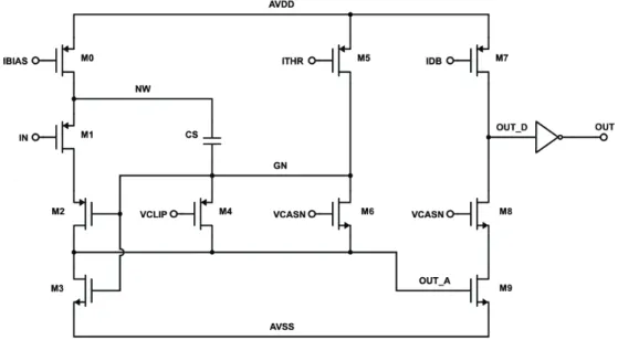
The analog front-end, shown in Fig. 3, was also changed to improve the threshold behavior. Initial measurements of the front-end circuit on the MALTA sensor revealed significant RTS noise preventing lower threshold settings. This was attributed to the M3 transistor being much smaller than on previous circuits. Further measurements confirmed the output conductance of this transistor was higher than expected, and caused gain degradation for the front-end. In addition it was found
PoS(Vertex2019)020
Figure 3: Schematic of the MALTA front-end.
that for lower threshold settings where the influence of this output conductance is larger, the spread on the gain and hence the threshold spread increased. To verify this assumption the MiniMALTA sensor includes sectors with the same M3 size as on MALTA and larger.
The MiniMalta came back from fabrication in January 2019. The chip features a 16 × 64 pixel matrix divided into two columns of four sectors of 8 ×16 pixels. The four sectors on the left half of the chip have the enlarged M3 transistor on the front-end of the chip, while the right half has the standard transistor. The bottom two sectors have the standard substrate with the continuous n-layer, the top two the n- gap, and the second from the bottom the extra deep p-well.
3. MiniMALTA Laboratory Measurements
Measurements on MiniMALTA confirmed that the larger M3 transistor size significantly de-creased the RTS noise, both before and after irradiation [6]. Fig. 4(a) and4(b) show measured charge threshold distributions and illustrate the lower threshold dispersion for the front-end with the larger M3 transistor. The mean of the measured ENC is comparable between the two sectors, however, there are fewer pixels with high noise in the modified sector as expected with a decrease in RTS. A dependence on irradiation was also measured. For the same sensor configuration, smaller thresholds and an increase in the ENC from approximately 10 e− to 20 e−were measured as well as an increase in the RTS noise in neutron irradiated samples with fluences up to 2× 10¹⁵neq/cm2
This irradiation dependence may be related to changes in capacitance of the irradiated sensor sub-strate.
In addition, the larger NMOS size also yielded a significantly larger gain and lower threshold charge threshold for the same settings. The gain of the front-end was measured. with 5.9 keV X-rays from an55Fe source. The measured amplitude spectra are shown in Fig. 5. The k-α peak of the standard and modified front-ends at 304.5 mV and 523.9 mV, respectively, showing that
PoS(Vertex2019)020
MiniMALTA design and measurement P. M. Freeman
100 200 300 400 500 600 700 ] -Threshold [e 0 20 40 60 80 100 120 140 160 Number of pixels
W2R11 (unirrad.) large trans. ) large trans. 2 /cm eq n 15 10 × W2R1 (1 ) large trans. 2 /cm eq n 15 10 × W1R3 (2 =22e σ =292e, µ fit to W2R11, =30e σ =217e, µ fit to W2R1, =29e σ =161e, µ fit to W1R3,
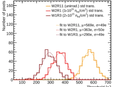
(a) Threshold distribution of the modified front-end [6] 100 200 300 400 500 600 700 ] -Threshold [e 0 20 40 60 80 100 120 140 160 Number of pixels W2R11 (unirrad.) std trans. ) std trans. 2 /cm eq n 15 10 × W2R1 (1 ) std trans. 2 /cm eq n 15 10 × W1R3 (2 =49e σ =569e, µ fit to W2R11, =50e σ =363e, µ fit to W2R1, =49e σ =290e, µ fit to W1R3,
(b) Threshold distribution of the standard front-end [6] 0 10 20 30 40 50 ] -ENC [e 0 20 40 60 80 100 120 140 160 Number of pixels
W2R11 (unirrad.) large trans. ) large trans. 2 /cm eq n 15 10 × W2R1 (1 ) large trans. 2 /cm eq n 15 10 × W1R3 (2
(c) ENC distribution of the modified front-end [6]. 0 10 20 30 40 50 ] -ENC [e 0 20 40 60 80 100 120 140 160 Number of pixels W2R11 (unirrad.) std trans. ) std trans. 2 /cm eq n 15 10 × W2R1 (1 ) std trans. 2 /cm eq n 15 10 × W1R3 (2
(d) ENC distribution of the standard front-end [6].
Figure 4: Measurements from threshold scans.
there is nearly double the gain with the enlarged transistor [6]. In the irradiated samples, the gain increases. The amplitude at the collection electrode, that is at the input of the readout circuit ("IN" in Fig.3), was also measured to have the same increase in gain after irradiation. This suggests that this post-irradiation effect may not be related to the front-end but instead to changes in capacitance to the substrate. The sensor capacitance may also play a role in the previously discussed radiation dependence of the threshold.
In spite of some unexpected radiation dependencies, laboratory measurements of MiniMALTA showed that the modified front-end had increased gain, lower thresholds, and better noise character-istics than the standard front-end. In order to demonstrate that these design changes improved the efficiency and charge collection in the pixel periphery, MiniMALTA was measured in test beams.
4. MiniMALTA Test Beam Results
The efficiency of MiniMALTA samples was studied at ELSA and DESY with beams of 3 to 5 GeV electrons, and in-pixel photon response at Diamond Light source with a precision-focused 8 keV X-ray beam [7,8,9].
PoS(Vertex2019)020
150 200 250 300 350 400 450 500 550 600 650 amplitude (mV) 0 50 100 150 200 250 number of hits 55Fe spectra from amplifier output
enlarged transistors standard transistors 7 = 304.5 mV < = 4.9 mV 7 = 523.9 mV < = 7.4 mV 7 = 523.9 mV < = 7.4 mV
(a) Amplitude spectrum of 55Fe measurements of
the standard and modified front-ends.
50 100 150 200 250 300 350 400 450 500 550 600 amplitude (mV) 0 50 100 150 200 250 300 350 400 number of hits
55Fe spectra from amplifier output before and after irradiation
unirradiated
irradiated 1e15 neq/cm2, 1 Mrad irradiated 2e15 neq/cm2, 2 Mrad
(b) Amplitude spectrum of 55Fe measurements of the
modified front-end of unirradiated and irradiated sam-ples [6].
Figure 5:55Fe measurements of MiniMALTA [6].
4.1 Efficiency Measurements
The efficiencies of unirradiated and irradiated MiniMALTA samples were measured using using the MALTA telescope. The MALTA telescope is a beam telescope composed of six collinear MALTA planes, each read out with a Xilinx VC707. A series of NIM modules were used to trigger on coincidences between planes and reconstructed tracks using the General Broken Lines (GBL) algorithm implemented in Proteus [10]. With the relatively large multiple scattering of electrons, GBL was essential for precise track reconstruction. For 3 GeV electrons, track residuals were approximately 14 µm in each plane coordinate [6].
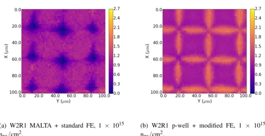
In Fig. 6(a)is a 2-D histogram of the efficiency from an irradiated MiniMALTA chip, W2R1. Each bin corresponds to a single pixel. The pixels on the edges of sectors have been excluded due to edge effects between the different sectors and multiple scattering. The blank sectors feature a PMOS reset instead of a diode reset, and could not be operated simultaneously with the other sectors. The efficiency in the unmodified sector of MiniMALTA is comparable to the efficiency measured at SPS and in the modified sectors there is significant improvement. Modification to only the front-end or only the substrate results in increased efficiency, though both are necessary to achieve the highest efficiencies. In the sectors which have both substrate and front-end design changes, the efficiency is above 98%.
In Fig. 6(b)are the mean efficiencies in each sector plotted as a function of threshold from two sensors, W2R1 and W4R2, both with with a fluence of 1 × 10¹⁵neq/cm2. For W4R2 the epitaxial
thickness for charge collection is 25 µm and for W2R1 it is 30 µm. As intended, with the modified front-end the chip was operational at lower thresholds and higher efficiency. Furthermore, at a given threshold, the efficiency is much better in the sectors with the substrate design changes.
4.2 X-ray Measurements at Diamond Light Source
At the Diamond Light Source, MiniMALTA was measured with a 8 keV X-ray beam in order to demonstrate the improvement in in charge collection in the periphery of the modified pixels.
PoS(Vertex2019)020
MiniMALTA design and measurement P. M. Freeman
(a) Efficiencies in different sectors of sample W2R1. The left half has the modified front-end, and the right half the standard. The bottom sectors have the standard substrate, the middle the extra deep p-well, and the top the n- gap,
φ = 1e15 neq/cm2[6]. 100 200 300 400 500 600 Threshold [e] 50 55 60 65 70 75 80 85 90 95 100 Efficiency [%] Large trans.
Large trans. + extra p-well Large trans. + n-gap Std trans.
Std trans. + extra p-well Std trans. + n-gap ) 2 neq/cm 15 10 × W2R1+W4R2 (1 m EPI) µ W4R2 (25 m EPI) µ W2R1 (30
(b) Efficiencies as a function of threshold, φ = 1e15 neq/cm2[6].
Figure 6: Efficiency results
MiniMALTA was mounted into a cold box on a motion stage with a 400 nm precision, moved the sensor in 2 µm steps, and recorded the number hits acquired in one second at each position. Hit maps were constructed from these data. The beam had a full width half maximum of 2 µm.
A photon energy of 8 keV was selected based on the mean number of electrons deposited in a thin silicon sensor. The mean deposited energy of minimum ionizing particles (MIPs) in silicon is 3.88 MeV/cm, so for the 20 to 25 microns depth of depleted epitaxial silicon in MiniMALTA, the mean deposited charge is between 7.7 keV and 9.7 keV [11].
In Fig. 7 are normalized hit maps for the sensor W2R1, which was neutron-irradiated to 1 × 10¹⁵n
eq/cm2. In the sector with the standard front-end and MALTA substrate (Fig. 7(a)), there
is a decrease in the relative number of hits in the region between pixels, similar to the decrease in efficiency in the MALTA chip measured at SPS. The sector with the modified front-end and extra deep p-well (Fig. 7(b)) has a decrease in the response in the pixel corners at 1 × 10¹⁵ neq/cm2,
but it is not as drastic. There are actually more hits between pixels than in the pixel centers for this sector. The sector with the n- gap substrate and modified front-end had comparable performance, and in both designs the charge collection in the periphery after irradiation has improved with the new substrate and front-end designs [12].
A more thorough analysis of the test beam is in [12]. In that reference, for the modified sectors of MiniMALTA, proton-irradiated sensors with a total ionizing dose (TID) of 70 MRad have similar photon response to unirradiated and neutron irradiated devices.
PoS(Vertex2019)020
(a) W2R1 MALTA + standard FE, 1 × 10¹⁵
neq/cm2.
(b) W2R1 p-well + modified FE, 1 × 10¹⁵
neq/cm2.
Figure 7: Hit maps from the Diamond test beam for different sectors of MiniMALTA.
5. X-Ray Irradiations
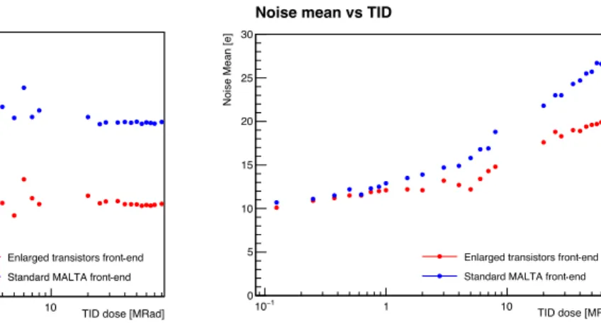
The gain and front-end behavior of MiniMALTA was characterized as a function of total ion-izing dose (TID) in a series of X-ray irradiations.
Fig.8shows the ENC and threshold distributions measured after each irradiation and indicates the modified front-end exhibits lower thresholds. The sectors with the modified front-end have lower thresholds for the same chip confiuration. For both sectors, there is a decrease in threshold as TID increases, with a slight increase in the threshold between 2 and 10 MRad followed by decrease and stabilization at higher levels of TID. The peak amplitudes measured from55Fe spectra follow a similar pattern, though as described in Sec. 3, the modified front-end has more gain. The noise measurements show a key difference in the radiation dependence of the two front-ends. Prior to irradiation, the mean ENC of each front-end is the same. This increases with TID for both designs, but more so for the standard; at 80 MRad, the ENC of the standard front-end has increased to 28 e−, while it is 21 e− for the modified. However, the mean values can be somewhat misleading as the unmodified front-end is biased by a small number of large values in the tail of the noise distribution.
Coupled with the results from Diamond described in [12], the X-ray irradiations show that MiniMALTA is fully operational after TID above the ALTAS requirement, and efficiencies are expected to be comparable to those of devices without TID.
6. Conclusions and Outlook
Measurements of the MiniMALTA prototype demonstrate significant improvement compared to the previous designs of the full-scale version of the chip. The measured efficiency at φ =1 × 10¹⁵ neq/cm2is above the required 97% for the ATLAS ITk, and precision focused X-ray measurements
demonstrate that there is an improvement in the charge collection in the pixel periphery after after neutron or proton irradiation with a large total ionizing dose [13]. Additionally, MiniMALTA is
PoS(Vertex2019)020
MiniMALTA design and measurement P. M. Freeman
1 −
10 1 10
TID dose [MRad] 0 100 200 300 400 500 600 700
Threshold Mean [e]
Enlarged transistors front end Standard MALTA front end
Threshold mean vs TID
-(a) MiniMALTA mean threshold as a function of TID.
1 −
10 1 10 TID dose [MRad]
0 5 10 15 20 25 30
Noise Mean [e]
Enlarged transistors front end Standard MALTA front end
Noise mean vs TID
-(b) MiniMALTA mean ENC as a function of TID.
1 −
10 1 10
TID dose [MRad] 0.1 0.2 0.3 0.4 0.5 0.6 0.7 0.8
Fluorescence peak to baseline [V]
Enlarged transistors front end Standard MALTA front end
Amplitude of FE target as a funcion of TID
-(c) MiniMALTA55Fe amplitude as a function of TID.
Figure 8: Gain, threshold, and noise measurements as a function of TID.
fully operational after a TID of 80 MRad. A telescope composed of MALTA sensors has been shown to have good beam telescope capabilities, including comparable tracking performance to widely-used telescopes in test beam experiments.
After these encouraging results on the small scale prototype MiniMALTA, a new version of MALTA has been fabricated with the sensor modifications, but still with the original front-end. Measurements on this MALTA version are now in progress. This version of the chip is produced on Czochralski silicon in addition to the production on epitaxial silicon. The Czochralski silicon is 300µm thick, allowing for much more depletion and therefore signal than the 30µm of epitaxial silicon. It also has a different concentration of impurities and that may result in an improvement in radiation hardness. A new design submission is also foreseen to include further improvements including a modified front-end.
Acknowledgments
We acknowledge Diamond Light Source for time on Beamline B16 under Proposal 22061. The measurements leading to these results have been performed at the Test Beam Facility at DESY Hamburg (Germany), a member of the Helmholtz Association (HGF). We acknowledge Dr. Ben
PoS(Vertex2019)020
Phoenix, Prof. David Parker, Amelia Hunter, and the operators at the MC40 cyclotron inBirming-ham (UK). Measurements leading to these results have been performed at the E3 beam-line at the electron accelerator ELSA operated by the university of Bonn in Nordhrein-Westfalen, Germany. This project has received funding from the European Union’s Horizon 2020 Research and Innova-tion program under Grant Agreement no. 654168 (IJS, Ljubljana, Slovenia). This project receives funding from the Postgraduate Research Scholarship Fund at the University of Birmingham (UK). This work is supported by the Turkish AtomicEnergy Authority (TAEK) under the project grant no. 2018TAEK(CERN)A5.H6.F2-20. All opinions and views in this paper are solely the responsibility of the author and do not necessarily represent those of the sponsor organization.
References
[1] W. Snoeys et al. A process modification for CMOS monolithic active pixel sensors for enhanced
depletion, timing performance and radiation tolerance. NIMA871 (2017) 90-96
[2] G. Aglieri Rinella on behalf of the ALICE collaboration, The ALPIDE pixel sensor chip for the
upgrade of the ALICE Inner Tracking System NIMA845 (2017) pg. 583-587
[3] I. Caicedo et al. The Monopix chips: Depleted monolithic active pixel sensors with a column-drain read-out architecture for the ATLAS Inner Tracker upgrade, 9th Workshop on Semiconductor Pixel Detectors for Particles and Imaging (PIXEL)JINST 14 (2019) C06006
[4] E. Schioppa, et al., Measurement results of the MALTA monolithic pixel detector, NIMA (2019). Available online (https://doi.org/10.1016/j.nima.2019.162404), 162404
[5] M. Munker et al. Simulations of CMOS sensors with a small collection electrode improved for a faster charge-collection and increased radiation tolerance, 9th Workshop on Semiconductor Pixel Detectors for Particles and Imaging (PIXEL), JINST 14 C05013 (2019)
[6] M. Dyndal et. al., Mini-MALTA: Radiation hard pixel designs for small-electrode monolithic CMOS sensors for the High Luminosity LHC, arXiv:1909.11987v1 (2019)
[7] Elektronen-Stretcher-Anlage. University of Bonn, Germany. Webpage: http:www-elsa.physik.uni-bonn.de/elsa_en.html
[8] Deutsches Elektronen-Synchrotron. Hamburg, Germany. Webpage: desy.de [9] Diamond Light Source, UK. Website: https://www.diamond.ac.uk/Home.html
[10] Kiehn, Moritz. (2019, March 7). Proteus beam telescope reconstruction (Version v1.4.0). Zenodo. http://doi.org/10.5281/zenodo.2586736
[11] M. Tanabashi et al. (Particle Data Group), Physics Rev. D 98 030001 (2018)
[12] M. Mironova et al., Measurement of the relative response of TowerJazz Mini-MALTA CMOS prototypes at Diamond Light Source, arXiv:1909.08392
[13] Collaboration, ATLAS, Technical Design Report for the ATLAS Inner Tracker Strip Detector, CERN. Geneva. The LHC experiments Committee (2017)
![Figure 5: 55 Fe measurements of MiniMALTA [6].](https://thumb-eu.123doks.com/thumbv2/123doknet/12847204.367637/8.892.466.746.140.362/figure-fe-measurements-of-minimalta.webp)