HAL Id: tel-00648593
https://tel.archives-ouvertes.fr/tel-00648593
Submitted on 6 Dec 2011HAL is a multi-disciplinary open access archive for the deposit and dissemination of sci-entific research documents, whether they are pub-lished or not. The documents may come from teaching and research institutions in France or abroad, or from public or private research centers.
L’archive ouverte pluridisciplinaire HAL, est destinée au dépôt et à la diffusion de documents scientifiques de niveau recherche, publiés ou non, émanant des établissements d’enseignement et de recherche français ou étrangers, des laboratoires publics ou privés.
Jonctions tunnel magnétiques à aimantation
perpendiculaire : anisotropie, magnétorésistance,
couplages magnétiques et renversement par couple de
transfert de spin
Lavinia Nistor
To cite this version:
Lavinia Nistor. Jonctions tunnel magnétiques à aimantation perpendiculaire : anisotropie, magné-torésistance, couplages magnétiques et renversement par couple de transfert de spin. Autre [cond-mat.other]. Université de Grenoble, 2011. Français. �NNT : 2011GRENY046�. �tel-00648593�
THÈSE
Pour obtenir le grade de
DOCTEUR DE L’UNIVERSITÉ DE GRENOBLE
Spécialité : Physique des MatériauxArrêté ministériel du 7 août 2006
Présentée par
Lavinia Elena NISTOR
Thèse dirigée par M. Bernard RODMACQ et co-dirigée par M. Bernard DIENY
préparée au sein du Laboratoire Spintec (INAC, CEA Grenoble) dans l'École Doctorale de Physique
Magnetic tunnel junctions with perpendicular
magnetization: anisotropy, magnetoresistance,
magnetic coupling and spin transfer torque
switching
Thèse soutenue publiquement le 7 Octobre 2011 devant le jury composé de:
M. James M. D. COEY
Prof., Trinity College, Dublin (Président)
M. Stéphane MANGIN
Prof., Université Henri-Poincaré, Nancy (Rapporteur)
M. Dafiné RAVELOSONA
D.R. CNRS, Institut d’Électronique Fondamentale, Orsay (Rapporteur)
M. Bernard RODMACQ
Ingénieur, Spintec, CEA Grenoble (Directeur de Thèse)
M. Bernard DIENY
Ingénieur, Spintec, CEA Grenoble (Co-Directeur de Thèse)
M. Olivier FRUCHART
D.R. CNRS, Institut Néel, Grenoble (Examinateur)
M. André THIAVILLE
D.R. CNRS, Laboratoire de Physique des Solides, Orsay (Examinateur)
M. Alain SCHUHL
Remerciements
Je tiens à remercier en premier celui qui m’a ouvert la porte vers la recherche dans le domaine du magnétisme : Viorel Pop, Professeur à l’Université Babes-Bolyai de Cluj-Napoca (Roumanie), qui a suivi avec beaucoup d’attention, de bons conseils et d'encouragements tout mon parcours scientifique à l’Université de Cluj et à l’Université Joseph-Fourier de Grenoble. Je vous remercie de m’avoir accueilli dans votre équipe depuis mes premières années de Faculté en me donnant la possibilité de faire mes premiers pas dans le métier de chercheur à vos cotés et surtout de m’avoir toujours soutenu dans mes choix. Merci pour votre confiance.
Je voudrais remercier Bernard Rodmacq, mon directeur de thèse à Spintec, pour toute sa patience, sa disponibilité, son enthousiasme et ses conseils. Je vous remercie d'avoir été à mes côtés dans mon apprentissage du métier de chercheur, de m’avoir toujours encouragée pour dire mes idées, de m’avoir appris à bien argumenter chaque manip, chaque point de mesure et de m’avoir initiée à la physique très appliquée à travers les brevets. Merci de m’avoir encouragée aussi à explorer pendant la thèse des problématiques plus fondamentales à coté d’un but plus appliqué. Merci pour votre disponibilité, les discussions avec vous m’ont apporté beaucoup au niveau scientifique et m’ont aidé à développer mon esprit critique.
Je voudrais aussi remercier Alain Schuhl, Directeur de SPINTEC jusqu'en 2010, et
Bernard Dieny, son adjoint et mon correspondant CEA, de m'avoir accueilli dans leur Laboratoire en me donnant la chance de découvrir un autre "monde" entre la physique fondamentale et les applications. Alain Schuhl, je vous remercie pour votre disponibilité et surtout pour vos conseils scientifiques mais aussi pédagogiques. Bernard Dieny, je voudrais vous remercier spécialement pour m’avoir suivi pendant ces années de thèse, pour vos conseils scientifiques concernant les articles et les présentations orales que j’ai faits pendant ma thèse. Je tiens aussi à remercier Jean-Pierre Nozières, actuel Directeur de Spintec, pour sa disponibilité, sa sincérité et les encouragements pour la suite de la thèse.
Je remercie James M.D. Coey d'avoir accepté de présider mon jury de thèse. Je remercie également Stéphane Mangin et Dafiné Ravelosona pour avoir accepté le travail de rapporteur pour ma thèse et pour leurs observations et suggestions. Merci également à Olivier Fruchart et
André Thiaville, et à tous les membres du jury, pour le temps qu’ils ont consacré à la lecture mon manuscrit de thèse, pour leurs questions intéressantes lors de ma soutenance et leurs observations et commentaires qui ont été très bénéfiques pour l’amélioration de ce manuscrit.
Merci à Stéphane Auffret pour toutes ses heures passées devant la machine de dépôt dans la salle blanche PTA, pour nous fabriquer les échantillons dont on avait besoin pour cette étude. Je te remercie Stéphane, pour la confiance que tu m’as montrée en m’apprenant à utiliser la machine de dépôt Actemium en tenant compte des problèmes techniques qu’elle avait. Merci Stéphane aussi pour les discutions scientifiques ou pas qui m’ont fait un grand plaisir.
Je tiens à remercier également Liliana Prejbeanu pour m’avoir donné la chance de faire de l’enseignement, pour toutes ses encouragements et conseils et discussions scientifiques et pédagogiques.
Je remercie aussi Mairbek Chshiev, pour toute sa disponibilité, sa patience pour discuter avec moi et m’aider à mieux comprendre mes résultats à travers la théorie. Merci Mair aussi de m’avoir laissé un peu explorer le monde des simulations de transport de spin et structure électronique des matériaux.
Pendant cette thèse j'ai utilisé différentes techniques. Je voudrais remercier pour leur disponibilité et leur aide pour résoudre des petits problèmes de manip à Stéphanie Pouget
pour la réflectivité de RX, Jean-François Jacquot pour le Squid et Marité pour m’avoir appris le process des jonctions tunnel à la PTA. Mes remerciements aussi au personnel de la salle blanche PTA.
Je voudrais aussi remercier Crocus Technology et spécialement Clarisse Ducruet, Céline Portemont et Lucian Prejbeanu pour leur collaboration sur certaines études et pour m’avoir fabriqué des échantillons et m’avoir laissé utiliser leur outil CAPRES pour faire des mesures de transport sur couches continues et pouvoir avancer plus vite (sans passer par l’étape lithographie) dans la fabrication des jonctions tunnel magnétiques.
Je remercie également tout le personnel du Laboratoire pour l'accueil et pour la bonne humeur et surtout les secrétaires qui m'ont beaucoup aidé avec tous les papiers qu’on a dû faire pendant ces 3 années de thèse.
Introduction:
MATERIALS. THE SPINTRONICS AGE.
MOTIVATION 1
References ... 7
Chapter I:
PERPENDICULAR MAGNETIC ANISOTROPY
AT MAGNETIC METAL/OXIDE INTERFACE
11
I-1. Origin of PMA in magnetic metal / oxide bilayers... 14
I-2. Experimental determination of perpendicular anisotropy ... 18
I-3. Thin films preparation ... 23
I-4. Pt/Co(CoFeB)/Oxide trilayers... 25
I-5. Growth of magnetic layers on oxides ... 32
I-6. Conclusions... 40
I-7. References ... 41
Chapter II:
ANISOTROPY AND TRANSPORT
PROPERTIES OF PERPENDICULAR MAGNETIC TUNNEL
JUNCTIONS 45
II-1. Magnetic tunnel junctions ... 49
II-2. Anisotropy properties of top and bottom electrodes in full stackings ... 60
II-3. Influence of the oxidation conditions of the barrier ... 70
II-4. Transport properties of perpendicular junctions ... 75
II-5. Correlation between anisotropy and magneto-resistance ... 80
II-6. Low effective demagnetizing field in planar magnetic tunnel junctions ... 87
II-7. Conclusions ... 90
Chapter III:
INDIRECT EXCHANGE COUPLING IN
PERPENDICULAR MAGNETIC TUNNEL JUNCTIONS 99
III-1. Indirect exchange coupling: theoretical models and experimental
determination ... 103
III-2. Indirect exchange coupling in perpendicular junctions ... 109
III-3. Variation of the antiferromagnetic coupling ... 115
III-4. Origin of the sign of interlayer coupling and of its variation ... 124
III-5. Coupling oscillations with top Co layer thickness ... 126
III-6. Conclusions ... 131
III-7. References ... 132
Chapter IV:
SPIN TRANSFER TORQUE SWITCHING IN
PERPENDICULAR MAGNETIC TUNNEL JUNCTIONS 137
IV-1. Spin Transfer Torque switching: theory and experiments ... 140
IV-2. STT switching of CoFeB/MgO/CoFeB/(Tb/Co) based pMTJ ... 148
IV-3. Conclusions ... 160
IV-4. References ... 162
Conclusion
167
References ... 170
Appendices
173
A-1. Today's recording media ... 175
A-2. Ellingham's diagrams... 177
A-3. Complementary magnetic measurements on in-plane junctions ... 178
A-4. Sub-micrometric junction processing at PTA ... 180
A-5. Scientific communications ... 185
A-6. French summary ... 187
A-6.1 French introduction ... 187
A-6.2 French summary ... 193
Introduction
MATERIALS. THE SPINTRONICS AGE. MOTIVATION
Materials, more or less sophisticated, are present in Man’s life since several thousand years. Man’s intelligence, in the need to improve his life condition, contributed to the evolution of the materials used in our daily life (from the simplest ones like the wood and stone to more complex ones like bronze and iron). The impact of materials in Man’s evolution was so strong than we can assert it helped to model civilisations. For instance, in the case of Hittites (18th century before Christ), the improvement of the technique to fabricate very good quality iron made them one of the most advanced and powerful civilisations of the antiquity and helped them to dominate the Mediterranean region
[Hum_04]. The appreciation of the materials
impact in Man’s history and evolution was illustrated in the History by naming each era after the material used:- stone age - 4500 bc - bronze age - 1700 to 0 bc - iron age – 1500 bc to 1950 ac
Nowadays we are more directed towards the use of functional materials (electronic materials, materials for optics, hydrogen storage materials) for technological applications but also for fundamental research because these materials are full of interesting phenomena to be understood and valorised.
We will focus in this manuscript on the electronic materials in which electrons are the first responsible for their physical properties. Some examples of electronic materials: magnetic materials, metals, insulators.
Magnetism is the property of materials which respond to an applied magnetic field and is related to the electron motion and parity of electrons in the atom. In a simplified picture according to Ampère and Oersted the electron motion (orbital motion around the nucleus, and spin motion around his axis) results in an electric current from which a magnetic field will rise. But spin comes out of quantum mechanics combined with relativity and can be detected by its
magnetic moment, m=g µB s, or the average spin of an ensemble of electrons in a given volume, the magnetization (M). Considering the electrons numbers, the Pauli’s law for filling the atomic energy levels (which allows one paired spin up and down electrons on each energy level in the atom) and spin-orbit coupling, one obtains the atomic momentum, J. So in the case of diamagnetic materials (which have no unpaired electrons and filled energy levels in their atoms, J=0) the magnetism will arise from the interaction between the external applied field and the electron motion in the atom through the Lentz law, resulting in a magnetic moment which will be opposite to the applied field. More interesting are materials with an atomic momentum like paramagnetic and ordered ferromagnetic or antiferromagnetic materials. In paramagnetic materials the uncompensated orbital momentum (L) and spin angular momentum (S) result in independent atomic moments contrary to the ferromagnetic materials which have cooperating atomic moments. This is why the response to an applied magnetic field will be different: paramagnetic materials will be ordered only in the presence of a magnetic field, while ordered materials will stay aligned even after the applied field is removed.
Electrons are also responsible for the metallic or insulating properties of materials. In this case electrons have the role of charge carrier. So in a simple picture one can distinguish such materials by their charge mobility. While metals present high electron mobility, insulators do not.
The fabrications techniques can change and model material properties. This is why they are an important factor in the materials evolution. Another example from history: the bronze discovery was due to the insertion of 10% tin (Sn) in copper (Cu) in order to decrease its melting temperature, making easier the elaboration of different objects. Today, joining together magnetic materials with metals or insulators by using new techniques of fabrication of thin films (with layer thicknesses of the order of the electron scattering length) like Molecular Beam Epitaxy or sputtering, made possible to evidence new physical phenomenon like:
- Interfacial perpendicular magnetic anisotropy (PMA) [Gra_68] - Giant MagnetoResistance (GMR) [Bai_88, Bin_89]
- Tunnel MagnetoResistance (TMR) [Moo_95]
- Oscillatory character of RKKY exchange coupling[Par_91].
All these fascinating phenomena consider the spin of the electron in addition to its charge, associating magnetism and electronic transport in a new research area: the spin electronics or Spintronics. Taking into account both charge and spin of electrons make the physics of materials more complex but gives an additional advantage to applications providing more possibilities to conceive new devices and reinvent the electronics.
Figure 1: Spintronics bricks: (a) Spin asymmetry; (b) Mott approximation; (c) Spin dependent diffusion; (d) Spin accumulation.
Spintronics is based on four effects (see Figure 1) which, when combined, are at the origin of all the properties observed in thin magnetic layers:
1) Spin asymmetry (d electrons): in the density of states for localized d electrons of a ferromagnetic material the number of spin up (↑) of d electrons is different from that of spin down (↓) ones.
2) Mott approximation: the electron spin is conserved (low probability of spin inversion after electron diffusion on the layer defects). As a consequence, two conduction channels exist in parallel for spin up and spin down [Mot_36].
3) Spin dependent diffusion (s electrons):as a consequence of the spin asymmetry there will be a different probability of diffusion for the s spin up and spin down electrons (conduction electrons) when they are parallel (P) or antiparallel (AP) to the magnetization of the layer. 4) Spin accumulation (s electrons): s electrons will be diffused at a magnetic/nonmagnetic
interface (because of the difference between the spin disequilibrium-equilibrium states). According to the Mott approximation s electrons will have large diffusion lengths.
Among all these properties of ferromagnetic-metal multilayers, the discovery of the GMR had the strongest impact on both fundamental and applied physics. From a fundamental point of view, GMR can be explained by the spin dependent diffusion of the electrons due to the relative orientation of the magnetisation in the magnetic layers. So when the layer’s magnetizations are parallel, only the electrons with the spin parallel to the magnetization can pass through the sample because they are weakly diffused resulting in a low resistance (Rlow) state. In the case when the layer’s magnetizations are antiparallel, both electrons with parallel/antiparallel spin will be diffused resulting in a high resistance (Rhigh) state. The large resistance variation between the AP and P orientation inspired the name of GMR. The schematic principle for a simplified case of two ferromagnetic layers (F1 and F2) separated by a
Figure 2: Schematic explanation of the GMR effect.
From an application point of view the GMR discovery offered a new concept for magnetic sensor device: the spin valve [Die_91]. Giving a much improved sensitivity at nanoscale than inductive or even anisotropic magnetoresistance sensors, the spin valves were rapidly integrated in the read/write heads of the hard disk drive (HDD) industry. This allowed a fast increase of the HDD areal density, as it can be observed in Figure 3, and inspired a new device for industrial applications, the Magnetic Tunnel Junction.
Figure 3: Read/Write heads technologies which contributed to the areal density increase in hard
disk drives [Fuj_06].
The magnetic tunnel junctions (MTJ) are spintronic devices derived from spin valves just replacing the metallic spacer by a very thin insulator (oxide) layer so that electrons can pass from one ferromagnetic layer to the other by tunnelling. In this case the spin filtering effect is dominant compared to spin diffusion and the result is a very high relative resistance variation called Tunnel MagnetoResistance (TMR). This is why MTJ devices have a higher output signal than spin valves, making them very attractive for industrial applications. The difference in the resistance values between the P and AP configuration of the magnetic layers can be used for binary coding so that new recording media applications or logic circuits can be imagined.
Today computers use four means of data storage: dynamic random access memory (DRAM), high density memory which needs to be constantly refreshed (high power consumption); static random access memory (SRAM, used in cache memories), with fast reading and writing cycles; Flash memories, non-volatile but with a low writing access; and hard disk drives (HDD), presenting high density but relying on moving parts, which impose size and speed limitations.
In the future, consumer needs for recording media will demand to combine high access speed, reduced noise, reliability, portability, non volatility and low power consumption in a smallest as possible chipwith high density. However, one also has to consider stability against thermal fluctuations and long-term data retention(Appendix 1).
Spintronics give us a candidate for this universal memory based on MTJ technology: the
Magnetic Random Access Memory (MRAM). MRAM is attractive for industrial applications because it could, in principle, replace all other kinds of memories. For instance using a MRAM in a computer, data could be loaded directly into the working memory and wouldn't have to juggle between main memory (SRAM) and hard disk. This could make possible instant-on systems and innovate in the computer architecture.
First MRAM architectures using in-plane magnetized thin films separated by a thin oxide provide some key advantages: the non volatility and unlimited read/write endurance (1015
read-write cycles), in addition to those of conventional RAM memories (speed of SRAM). The energy used for operating (data retention for writing/reading process) is much smaller than that of FLASH because the time required per operation is much shorter. But, even if MRAM writing technique seems the simplest one using an applied field to switch the free layer magnetization, the architecture required is complicated and requires a lot of space making impossible to reach high densities. In addition, Field Induced Magnetic Switching MRAM architectures reach their limits when the cell size is reduced below 100 nm. Decreasing the cell size will increase the current density necessary to produce the switching field and also the write power, the selection errors for writing the memory cells will also increase, as the impact of the thermal fluctuations on the data stability. A 4Mb-MRAM was commercialized by Freescale Motorola (now EverSpin) in 2006 [Eve_06] and finds applications in satellite, aerospace, automotive/ telecommunications industries or memory embedded in controllers or printers.
A high density/stable/fast MRAM memory is the dream to the universal memory which could be used in all applications and replace all different recording media and memories of present times. But it requires a new MRAM technology.
A new physical phenomenon for magnetization switching, the spin transfer torque switching (STT) predicted by Slonczewski in 1996 [Slo_96, Ber_96] and first measured in spin valves [Kat_00, Sun_02, Puf_03], gives the possibility to reach storage densities of DRAM’s. An STT-MRAM architecture can be imagined and can bring considerable advantages: no more addressing errors because only the pillars traversed by the pulse current will be written; increasing the memory density, by suppressing write line, enables 1 Transistor-1 MTJ per cell similar to DRAM and makes possible the MTJ cell size reduction.
In the case of nano-magnetic elements with in-plane magnetization, the thermal stability limit is not related to the current induced switching parameters, but to their shape. In materials without preferred in-plane axis for the magnetization (without crystalline anisotropy), a specific elliptical shape is required to stabilize the magnetization along the long in-plane axis in order to minimize the magnetostatic energy. Reducing cell size makes impossible to keep the elliptical shape and to prevent from magnetization curling due to thermal fluctuations. One solution is to define the magnetization direction of the free layer by coupling it to an antiferromagnetic layer (AF). The switching of the free layer is realized by heating the MTJ cell above the blocking temperature of the antiferromagnet. Based on this phenomenon Spintec proposed a new write technique based on thermally-assisted spin transfer torque switching (STT-TAS-MTJ) [Pre_04, Oun_02, Noz_06, Her_10].
Using materials with out-of-plane anisotropy could be an alternate solution to keep the magnetization along one well-defined axis in MTJ and enhance the robustness against thermal fluctuations [Mor_06, Car_08, Yoo_05]. The size and shape limitations of planar MTJ elements with respect to magnetization curling are eliminated by using p-MTJs. Furthermore studies [Man_06, Nak_08] have shown that STT perpendicular structures may present lower critical switching currents and higher STT efficiency.
These new out-of-plane MTJ elements are promising for industrial applications and interesting for fundamental physics. The pMTJ combine both magnetic properties as out-of-plane anisotropy of the layers and tunnel transport properties across an insulator barrier. In conventional MTJ the high TMR performances are given by the good match between the crystal structure and texture of barrier and electrodes, interfaces quality, low roughness of the barrier. PMA can have different origins, either bulk (in hcp CoCrPt, heavy rare earth/transition metal alloys, or FePt L10 ordered alloys, or interfacial (in Pt/Co, Pd/Co, or Co/Ni multilayers). It has also been observed that a quite large PMA can be induced at the interfaces between the ferromagnetic electrodes and an oxide [Mon_02, Rod_03]. One can take advantage of this PMA from the oxide magnetic electrode interface to fabricate out-of-plane MTJ.
In conclusion pMTJ are very promising for increasing storage areal density, still keeping good data stability and low power consumption. But even if the stability problem seems to be solved other questions can arise:
1) Are nanofabrication techniques able to produce very small nanopillars having the size of one transistor of our days (30nm)?
2) Can we fabricate adapted electronics around a 1T-STT-MTJ cell?
STT-pMRAM will be able to compete with FLASH memories and HDD if these technical aspects are solved at similar production cost. Otherwise MRAM will be used in special markets like Battery-Backed SRAM replacement and would be attractive in applications where speed and permanent data storage are needed, eliminating the use of combined memories. Some examples of applications are the replacement of components of server systems, networking and data-storage devices, home-security systems and computer printers. The consequences are enormous considering the circuit size reduction, low system energy resulting in increased battery life, enhanced performance by improving efficiency of data transfer (the computer start speed). Even more, with MTJ it will be possible to take advantage of precessional dynamics for low power operation or to obtain tuneable radiofrequency oscillators leading to new RF devices for the mobile phone industry.
This thesis summarizes all the efforts done during the last three years, from the fabrication of pMTJ elements to the demonstration of low STT switching currents obtained by using outofplane magnetic anisotropy.
The engineering of pMTJ is a real challenge and a difficult task because good TMR and PMA properties will impose constraints and limit the working window of the device. It also demands a good understanding of PMA and TMR origins, and a good mastering of the thin film growth and characterization techniques in order to be able to optimize the characteristics of materials to obtain their best properties in a given sample. Thin film growth and characterization showed me the physics complexity and wealth of structures made of different materials with different properties. One can obtain a lot of combinations of these properties using different materials, changing their layers thicknesses, performing annealing treatments, applying magnetic fields or current pulses.
We will present here the most significant studies and results in four chapters. Chapter I will be dedicated to the fabrication of materials having PMA contribution also from the interface with an oxide. Both magnetic metal/oxide and oxide/magnetic metal structures will be studied. The PMA origin in these two kinds of materials will be studied by varying different parameters like nature of magnetic material, annealing temperature, layer thicknesses. Chapter II will be dedicated to full pMTJ structures and two kinds of materials will be presented: those with very high PMA based on Pt/Magnetic Metal/Oxide and those with low PMA like Ta/Magnetic Metal/Oxide. Magnetic and transport properties of both structures will be studied in order to choose the best candidate for the MRAM applications. A correlation between TMR and PMA was observed and it helped to confirm the PMA origin from the magnetic metal/oxide interface. Chapter III is a more fundamental study of pMTJ and concerns interlayer exchange coupling in the presence of out-of-plane anisotropy. A detailed study was made comprising annealing
temperature and layers thickness dependence of the coupling in order to understand its origin. Finally the STT-pMTJ concept will be validated in Chapter IV, after sub-micrometric patterning of magnetic tunnel junctions.
References
[Bai_88] M.N. Baibich, J.-M. Broto, A. Fert, F. Nguyen Van Dau, F. Petroff, P. Etienne, G. Creuzet, A. Friederich and J. Chazelas, Giant magnetoresistance of (001)Fe/(001)Cr magnetic
superlattices, Phys. Rev. Lett. 61 (1988) 2472.
[Ber_96] L. Berger, Emission of spin waves by a magnetic multilayer traversed by a current, Phys. Rev. B 54 (1996) 9353.
[Bin_89] G. Binasch, P. Grünberg, F. Saurenbach and W. Zinn, Enhanced magnetoresistance in
layered magnetic structures with antiferromagnetic interlayer exchange, Phys. Rev. B 39 (1989) 4828 (R).
[Car_08] B. Carvello, C. Ducruet, B. Rodmacq, S. Auffret, E. Gautier, G. Gaudin and B. Dieny,
Sizable room-temperature magnetoresistance in cobalt based magnetic tunnel junctions with out-of-plane anisotropy, Appl. Phys. Lett. 92 (2008) 102508.
[Die_91] B. Dieny, V.S. Speriosu, B.A. Gurney, S.S.P. Parkin, D.R. Wilhoit, K.P. Roche, S. Metin, D.T. Peterson and S. Nadimi, Spin-valve effect in soft ferromagnetic sandwiches, J. Magn. Magn. Mat. 93 (1991) 101.
[Eve_06] http://everspin.com/press.php?ppo=2006&qtype=press
[Fuj_06] Storage Systems and HDD Technologies, Fujitsu Sci. Tech. J. 42 (2006) 122.
[Gra_68] U. Gradmann and J. Müller, Flat ferromagnetic epitaxial 48Ni/52Fe(111) films of few
atomic layers, Phys. Stat. Sol. 27 (1968) 313.
[Her_10] J. Alvarez-Hérault, PhD Thesis, Grenoble University (2010).
[Hum_04] R.E. Hummel, Understanding Materials Science - History, Properties, Applications, 2nd Edition, Springer-Verlag, New York, (2004).
[Kat_00] J.A. Katine, F.J. Albert, R.A. Buhrman, E.B. Myers and D.C. Ralph, Current-driven
magnetization reversal and spin-wave excitations in Co/Cu/Co pillars, Phys. Rev. Lett. 84 (2000) 3149.
[Man_06] S. Mangin, D. Ravelosona, J.A. Katine, M.J. Carey, B.D. Terris and E.E. Fullerton,
Current-induced magnetization reversal in nanopillars with perpendicular anisotropy, Nature Mater. 5 (2006) 210.
[Mon_02] S. Monso, B. Rodmacq, S. Auffret, G. Casali, F. Fettar, B. Gilles, B. Dieny and P. Boyer,
Crossover from in-plane to perpendicular anisotropy in Pt/CoFe/AlOx sandwiches as a
function of Al oxidation: A very accurate control of the oxidation of tunnel barriers, Appl. Phys. Lett. 80 (2002) 4157.
[Moo_95] J.S. Moodera, L.R Kinder, T.M. Wong and R. Meservey, Large magnetoresistance at
room temperature in ferromagnetic thin film tunnel junctions, Phys. Rev. Lett. 74 (1995) 3273.
[Mor_06] A. Morisako and X.X. Liu, Sm-Co and Nd-Fe-B thin films with perpendicular anisotropy
for high-density magnetic recording media, J. Magn. Magn. Mater. 304 (2006) 46. [Mot_36] N.F. Mott, The electrical conductivity of Transition Metals, Proc. Roy. Soc. A 153 (1936)
699.
[Nak_08] M. Nakayama, T. Kai, N. Shimomura, M. Amano, E. Kitagawa, T. Nagase, M. Yoshikawa, T. Kishi, S. Ikegawa and H. Yoda., Spin transfer switching in TbCoFe/CoFeB/MgO/CoFeB/TbCoFe magnetic tunnel junctions with perpendicular magnetic anisotropy, J. Appl. Phys. 103 (2008) 07A710.
[Noz_06] J.-P. Nozières, B. Dieny, O. Redon, R.C. Sousa and I.L. Prejbeanu, Magnetic memory with
a magnetic tunnel junction written in a thermally assisted manner, and method for writing the same, US Patent 7,411,817 (2006).
[Oun_02] K. Ounadjela, B. Dieny and O. Redon, High density MRAM using thermal writing, US Patent 20020281603 (2002).
[Par_91] S.S.P. Parkin, Systematic variation of the strength and oscillation period of indirect
magnetic exchange coupling through the 3d, 4d, and 5d transition metals, Phys. Rev. Lett. 67 (1991) 3598.
[Pre_04] I.L. Prejbeanu, W. Kula, K. Ounadjela, R.C. Sousa, O. Redon, B. Dieny and J.-P. Nozières,
Thermally assisted switching in exchange-biased storage layer magnetic tunnel junctions,
IEEE Trans. Magn. 40 (2004) 2625.
[Puf_03] M.R. Pufall, W.H. Rippard and T.J. Silva, Materials dependence of the spin-momentum
transfer efficiency and critical current in ferromagnetic metal/Cu multilayers, Appl. Phys. Lett. 83 (2003) 323.
[Rod_03] B. Rodmacq, S. Auffret, B. Dieny, S. Monso and P. Boyer, Crossovers from in-plane to
perpendicular anisotropy in magnetic tunnel junctions as a function of the barrier degree of oxidation, J. Appl. Phys. 93 (2003) 7513.
[Slo_96] J.C. Slonczewski, Current-driven excitation of magnetic multilayers, J. Magn. Magn. Mater. 159 (1996) L1.
[Sun_02] J.Z. Sun, D.J. Monsma, D.W. Abraham, M.J. Rooks and R.H. Koch, Batch-fabricated
spin-injection magnetic switches, Appl. Phys. Lett. 81 (2002) 2202.
[Yoo_05] I. Yoo, D.K. Kim and Y.K. Kim, Switching characteristics of submicrometer magnetic
PERPENDICULAR MAGNETIC ANISOTROPY AT MAGNETIC
METAL/OXIDE INTERFACE
I-1. Origin of PMA in magnetic metal / oxide bilayers ... 14
I-2. Experimental determination of perpendicular anisotropy ... 18
I-3. Thin films preparation ... 23
I-4. Pt/Co(CoFeB)/Oxide trilayers ... 25
I-4.1 Natural oxidation ... 25
I-4.2 RF deposition of MgO ... 27
I-4.3 Comparison between Co and CoFeB ... 28
I-4.4 RF deposition of MgO in different machines ... 29
I-4.5 Influence of Pt buffer ... 29
I-4.6 Influence of capping layer ... 30
I-5. Growth of magnetic layers on oxides ... 32
I-5.1 Growth of magnetic materials on thermally oxidized SiO
2... 32
I-5.2 Growth of Co on different oxides ... 33
I-5.2.A Growth of Co on thermally oxidized SiO
2... 33
I-5.2.B Growth of Co on different oxides prepared by sputtering ... 35
I-5.2.C Comparison with Pt/Co/Ox and Pt/Co/Pt structures ... 36
I-6. Conclusions ... 40
I-7. References ... 41
Chapter I
PERPENDICULAR MAGNETIC ANISOTROPY AT MAGNETIC
METAL/OXIDE INTERFACE
In magnetic materials the spontaneous magnetization can have preferred orientation axes. This anisotropy can be quantified as a magnetic energy dependence on the magnetization direction. More precisely the orbital momentum of the electrons (L) is coupled to the lattice by electrostatic interactions with the charge distribution of ions in materials (crystalline electric field E). Since the orbital momentum direction is established by crystal field it will also affect the spin (S) magnetic moment through the spin-orbit interaction resulting in the magnetization alignment along the preferred lattice axis. This is known as the magnetocrystalline contribution to the anisotropy. When the magnetization lies perpendicular to the layer (sample) plane we talk about perpendicular magnetic anisotropy (PMA).
PMA can have different origins, either bulk (in hcp CoCrPt, heavy Rare Earth-Transition Metal, or L10 FePt ordered alloys), or interfacial (in Pt/Co, Pd/Co, or Co/Ni multilayers). In this
latter case it has also been observed that a quite large PMA can be induced at the interface between a ferromagnetic electrode and an oxide [Mon_02].
Materials with PMA already proved their advantage for increasing storage density in Hard Disk Drives. Another application is envisaged in the case of MTJ based memories taking use of the anisotropy arising from the interface between the magnetic layers and the oxide barrier. From a basic point of view perpendicular magnetized materials are fascinating and can be used to investigate field/current induced domain wall motion, spin torque switching phenomena, control of magnetic properties by an applied electric field [Man_06, End_10, Ike_10, Mir_10, Wei_07]. But this needs a good understanding of the anisotropy origin in thin films, especially at the magnetic metal/oxide interface.
This chapter will present the essential PMA properties of magnetic metal/oxide and oxide/magnetic metal structures. First the origin of PMA at magnetic metal/oxide interface will be discussed. We will then present the principles of PMA determination in thin magnetic films.
I-1. Origin of PMA in magnetic metal / oxide bilayers
In magnetic thin films, the interfaces have a high impact on their magnetic properties, due to the reduced bulk contribution. This is even more relevant in the case of the perpendicular magnetic anisotropy (PMA) for which the interface between the magnetic and non-magnetic layer is the driving mechanism, as predicted by Néel [Née_54] and experimentally observed several years later [Gra_68]. In a very simple picture the measured effective anisotropy energy (KEff) will
have two major contributions (Figure I-1), the volume anisotropy (KV) and the surface/interface
anisotropy (KS/KI), whose relative contribution increases as the thickness t of the magnetic film
decreases.
The volume anisotropy in transition metal thin films has two major contributions: magnetocrystalline volume anisotropy (KV) and shape anisotropy (KD). The magnetocristalline
anisotropy in the case of Co, Fe and Ni metals is due to the spin-orbit interactions. The orbital magnetic moment (mOrb) is usually a small contribution to magnetism in 3d transition (due to the
orbital moment quenching), resulting in low magnetocrystalline anisotropy contribution to the volume anisotropy (for Co KV=4.1 105 J/m3 (4.1 106 erg/cm3))
[Daa_94].
For these materials thedipolar interaction energy (which depends on the orientation of the magnetization relative to the crystal axes) only contributes to the shape anisotropy since the sum of the dipole–dipole energies cancels in symmetric crystals (Fe, Ni cubic, and Co hcp with low c/a ratio deviation
[Daa_90]).
In thin films the long range magnetic dipolar interaction is sensitive to the outer boundaries of the sample giving rise to strong demagnetizing fields when the magnetization is tilted out of the film plane. In the absence of uniaxial anisotropy contribution, magnetization prefers to lie parallel to the film plane in order to minimize the magnetic energy.These contributions to the effective anisotropy can be expressed as follows:
t K K M K K s s s V eff 2 1 2 2
Equation I-1From this empirical expression, one can see that the interfacial contribution of the anisotropy increases when the magnetic layer thickness (t) decreases. The interfacial anisotropy term KS1+KS2 is the sum of the contributions from both interfaces and could only be observed
thanks to the improvement of deposition techniques which enabled the fabrication of very thin layers.
At the interface (surface) the crystal continuum is broken, so atoms from the interface (surface) have a different environment compared to those in the bulk (Figure I-1). Considering this fact, Néel [Née_54] predicted that the effective anisotropy of thin films should be different from that in the bulk due to the interfacial anisotropy contribution. However, Neel’s approach is based on the simple pair interaction model (localized molecular orbitals) and is not the most appropriate for 3d transition metals like Co, Fe, Ni. The itinerant electron model (band model) introduced by Gay and Richter [Gay_86] to explain PMA in thin films gives a more appropriate
picture taking into account the position of the Fermi level together with the broken crystal symmetry at the interface/surface.
Let us first focus on the simplest case, surfaces.Bruno [Bru_89] predicted for Co, Fe, Ni monolayers a surface anisotropy of the order of 1 erg/cm2 which strongly depends on the
crystal-field parameters and on the filling of the 3d bands. Because of the strongly reduced symmetry at the surface, it will result in much larger shifts (Δ) in the d orbitals energy than in bulk materials (high symmetry) (Figure I-2). More precisely, the absence of coordination atoms results in a reduction of the 3d band which will more affect the out-of-plane orbitals than the in-plane ones (see Figure I-2 for d orbitals). As a result, the bands population needs to be reconfigured by a charge transfer from the in-plane to the out-of-plane levels, thus changing the coulombian energy which will split the levels.
The picture is more complicated in the case of interfaces due to the presence of different
kinds of surrounding atoms. This is why at the interface one has to consider at the same time not only a change in the bulk symmetry but also a change of the nature of coordination (surrounding) atoms. Two examples are presented for different materials at the Co(Fe) interface, Pt with a strong spin-orbit coupling and a strong crystal field, and O with low spin-orbit coupling.
The presence of heavy atoms like Pt (or Pd) at the Co interface will induce a strong hybridization of 3d Co orbitals with 5d Pt orbitals [Nak_98] which, combined with the strong spin-orbit coupling of Pt, will produce an increase of the Co orbital momentum [Wel_94], making possible to orient the spin momentum perpendicular to the interface. In more details, the interface hybridization can be viewed as an effective uniaxial crystal field acting on the Co/Pt interfacial atoms and modifying the material's band structure. At the Co interface side, the crystal field defines both in-plane orbitals dxy and dx2-y2 states and out-of-plane orbitals with dyz and dxz states near the Fermi energy level.The spin-orbit coupling will split both in-plane and out-of-plane states at the interface. The energy separation for dxy and dx2-y2 states is smaller than in bulk Co (due to the broken symmetry at the interface) but also smaller than the spin-orbit coupling separation in out-of-plane orbitals dyz, dxz. Due to the strong splitting in out-of-plane orbitals,
the Co out-of-plane perpendicular orbital momentum will be enhanced. Wang et al [Wan_93] showed that the d-d bonding between Co and Pd ismediated by dyz, dxz orbitals and
predicted even stronger bonding with Pt or Au since in these materials the spin-orbit interaction is larger. The crystal field effect on interfacial Pt layer will shift towards lower energies the Pt 5d bands of spin parallel to the Co majority spin, resulting in a Pt spin momentum parallel to that of Co (Ms(Pt) // Ms(Co)). The large Pt orbital momentum contributes to the interfacial Pt layers
magnetic moment via a strong spin-orbit coupling, thus aligning it parallel to the Co total momentum.
Figure I-2: Co d orbitals and effect of the surface/interface broken symmetry (no coordination
In conclusion PMA at Co/Pt interface is due to the 3d-5d hybridization combined with spin-orbit coupling:
for Co layers this results in a strong splitting of in-plane and out-of-plane orbitals favouring the lowest energy for the out-of-plane orbital.
for Pt layers the effect is the occurrence of a magnetic moment at the Pt interface aligned with the Co magnetic moment.
The interfacial perpendicular anisotropy reported in the case of Co/Pt (Pt, Pd, Au, W, Mo) multilayers [Bro_89, Yoo_05] is principally due to a heavy metal layer (having a strong spin-orbit coupling) present at the interface. According to this observation it was believed that the presence of heavy metal at the magnetic metal interface is essential to obtain the PMA.
Recently a PMA interfacial contribution from the MagneticMetal/oxyde interface has been observed [Mon_02, Rod_03] despite the weak spin-orbit coupling. Experiments showed that this phenomenon is quite general [Man_08a, Rod_09, Nis_09, Ike_10] since it was observed at the interface between various magnetic transition metals and oxide layers and is independent of the crystalline structure of the oxide layers. In addition, X-ray photoemission spectroscopy [Man_08b] showed that oxygen plays an essential role in the PMA at magnetic metal-oxide interface by the formation of Fe(Co)-oxygen bonds. For a better understanding of the PMA origin at the Magnetic Metal/oxide interfaces an ab initio study was realized taking into account the weak spin-orbit coupling [Yan_11].
The origin of the large PMA is ascribed to the combination of several factors: degeneracy lift of out-of-plane 3d orbitals due to the weak spin-orbit coupling,
hybridizations between dz2 and dxz and dyz 3d orbitals induced by weak spin-orbit
interactions
hybridizations between Fe-3d and O-2p orbitals at the interface between the transition metal and the insulator.
The strong overlap between Fe 3d and O 2p orbitals modifies the band structure giving rise to a strong crystal field at the interface. In Figure I-3(middle column) one can clearly see the band levels for the 3d Fe and 2p O orbitals, containing levels (blue/green levels) resulting from the hybridization of the Fe dz2 and O pz orbitals near the Fermi level energy. Even a low spin-orbit coupling is enough to split the Fe(Co) band levels dxz, dyz, dz2 and O pz around Fermi energy in either the in-plane magnetization (right column in Figure I-3), or the out-of-plane magnetization configuration (left column in Figure I-3). After splitting, band positions corresponding in energy for dz2, dxz, dyz levels become hybridized, resulting in the appearance of additional levels for both dz2 and dxz,yz orbitals represented by numbers showing the percentage of the corresponding orbital character components within Wigner-Seitz spheres. For the out-of-plane magnetization orientation (left columns), the additional dz2 levels with 5, 2 and 44 percentage (red lines) originate from dxz,yz orbital character due to SOI and the additional dxz,yz band with 8 percents (blue line) comes from dz2 orbital. In addition for the out-of plane magnetization orientation (left subcolumns) of Fe dz2 we also observe energy levels with O-pz character (red levels) since the Fe dz2 orbitals have already been hybridized with the O pz ones.
In conclusion PMA at metal/oxide interface comes from the combination of the Fe-O bond formation resulting in the mixing of dz2 and pz levels and the weak spin-orbit coupling which will split the levels in the dxz, dyz, dz2 and pz and especially mix the dxz and dyz orbitals with the dz2 ones.
So far, it was assumed that the layers have ideal flat interfaces. In reality, films cannot be grown perfectly even using epitaxial techniques. This leads to roughness and/or interdiffusion at the interface which will modify the magnetic properties.
Figure I-3: Fe-O hybridization and spin-orbit coupling effects at Fe/O interface. Three sub-columns in each column show the band levels for out-of-plane (left) and in-plane (right) orientation of the magnetization as well as for the case with no spin-orbit interaction included (middle).
The effect of roughness on the dipolar anisotropy has been studied theoretically by Bruno [Bru_88]. He used an ideal rough surface (epitaxial layers case) which can be characterized by the roughness height h (which is the mean square deviation from the ideally flat surface) and the correlation length λ (the average lateral size of flat areas on the surface, terraces). Roughness creates in-plane demagnetizing fields at the edges of terraces reducing the shape anisotropy. The anisotropy contribution resulting from the roughness will, therefore, always be positive (favouring PMA). In addition, due to its presence at the interfaces only it will scale as 1/t. But roughness will also introduce step atoms at the interface. Contrary to terraces each step atom contributes to a decrease of the anisotropy. In general the roughness always reduces the anisotropy, it is just a matter of number of step atoms relative to the number of terrace atoms. However for sputtered samples, roughness effects may greatly alter the magnetic surface anisotropy.
The interdiffusion between layers, caused by the nature of the materials (immiscibility) or by annealing, is always detrimental to the interface anisotropy. For example it was experimentally observed [Man_08a, Rod_09, Nis_10] and calculated [Yan_11] that over/under-oxidation of the magnetic material/oxide interface will strongly reduce the interface anisotropy. In the case of over-oxidation at the interface (additional oxygen at the Co interface) the Fe dz2 and O pz orbitals will no more mix due to the charge redistribution induced by the additional oxygen and the spin orbit coupling will cause stronger splitting for dxz,yz states with in-plane orientation than with out-of-plane. The case of under-oxidized interface is characterized by no overlap between the Fe dz2 and O pz orbital and dxz,yz orbitals, and higher splitting for out-of-plane magnetization orientation compared to the in-plane one. Anisotropy in the under-oxidized case will be higher than in the over-oxidized case but much lower than in the case of ideal Fe/MgO interfaces. All this underlines the importance of the interface quality.
I-2. Experimental determination of perpendicular anisotropy
The effective anisotropy energy Keff is the energy required to align the magnetization along the hard magnetization axis and it can be calculated by the difference in areas of the M(H) curves measured along the hard and easy axis directions [Joh_96]:
Keff
M
dH
M
dH
easy axis
hard axis
Equation I-2Keff is usually taken as positive for out-of-plane magnetization. In the case of a linear M(H) variation along the hard axis, the saturation field Han can be used to extract Keff using Keff= Han MS/2, where MS is the saturation magnetization determined from VSM or SQUID measurements. Along the easy axis, only the reversible magnetization curve has to be considered as shown in Figure I-4. In the case of perpendicular magnetization with a multidomain structure in zero applied field, and because of the magnetostatic interactions between domains, saturation fields will have no direct relation with KEff. However KEff can still be determined from the differential area. In practice the anisotropy measured along the hard axis is always much larger than that measured along the easy axis, which can usually be neglected, except near the transition from perpendicular multidomain to in-plane magnetization, which however occurs on a very narrow thickness range.
According to Equation I-1, a plot of Keff t versus t, where t is thickness of the magnetic layer, should give a straight line if the total anisotropy can be reasonably separated into a volume and interface contribution. Figure I-5 gives an example of such a plot in the case of Co/Pd multilayers [Bro_91]. The interface anisotropy KS1+KS2 is usually noted as 2KS in the case of multilayers, where one supposes that both bottom and top interfaces contribute equally to the anisotropy. This is not straightforward if one considers possible differences between the growth of the magnetic material on the metallic spacer and the growth of the metallic spacer on the magnetic material. In our case it is even more questionable since we are dealing with two different interfaces (Pt/Co and Ox/Co for example). We will however, for convenience, call 2KS the total interface anisotropy KS1+KS2.
Figure I-4: (a) Magnetization measurements along easy and hard axis in the case of a sample with
out of plane magnetization; (b) KEff determination by the the difference between areas above
The interface anisotropy 2KS is obtained from the vertical axis intercepts, whereas the difference between the volume anisotropy and demagnetizing energy contribution (KV-2πMS2) is given by the slope of the curve. The effective anisotropy can be:
a) positive (Keff > 0): the interface anisotropy contribution 2KS outweighs the volume contribution (KV-2πMS2), resulting in a perpendicularly magnetized system. The strong demagnetizing fields which are created when tilting the magnetization out of the film plane, and which are usually responsible for the orientation of the magnetization parallel to the film plane, are overcome.
b) zero (Keff = 0), which marks the transition of the magnetization from out-of-plane to in-plane for a given magnetic thickness called critical thickness.
c) negative (Keff < 0), when the volume term dominates and the magnetization is in-plane. The volume contribution KV, which can be either positive or negative, is usually much smaller than the demagnetizing term, leading generally to a negative slope of the curves. Increasing the 2KS/t term (increasing KS and/or decreasing thickness) is thus the only way to obtain perpendicular magnetization.
There are different techniques sensitive to the magnetization which can be used to determine the magnetization variation either along the easy axis (coercive field) or the hard axis (magnetic anisotropy): magnetometry techniques (VSM and SQUID), magneto-optical techniques (Kerr Effect) and magneto-transport techniques (magnetoresistance or Hall Effect). Each technique has advantages and drawbacks, and the choice of the technique will depend on both sample composition and expected information.
Magnetometry measurement is in principle the best choice, since it gives an absolute values of the magnetization. However, the sensitivity is limited to magnetic thicknesses larger than about 1 nm. In addition, since it is a global measurement, all magnetic contaminations (substrate, sample holder) will contribute to the signal. SQUID measurements lead to a much better sensitivity, but suffer from the same contamination problems. It is also a very time-consuming technique.
Magneto-optical techniques are insensitive to external parasitic signals (except for possible surface contamination). The sensitivity to thin magnetic layers is very good, and measurements fast. However, because of the limited penetration depth of the laser radiation, the signal of buried magnetic layers will be small, especially when using capping layers made of heavy metals. In the case of multiple magnetic layers, the relative amplitudes of the Kerr signals will not
Figure I-5: Effective magnetic anisotropy times Co thickness versus Co thickness in Co/Pd multilayers: (a) Out-of-plane anisotropy; (b) Critical thickness; (c) In-plane anisotropy. The vertical axis intercept equals the sum of both interface anisotropies, whereas the slope gives the volume
give the real ratio of magnetizations.
Transport measurements, especially Hall effect, are sensitive to the perpendicular component of the magnetization. Hall effect is a very sensitive technique, but only when the magnetic layer is in contact with metals such as Pt or Pd. As an example, a Co layer sandwiched between two oxide layers will gives almost no Hall signal. The Hall amplitude will thus depend on the magnetization, but also on the Hall coefficient, which is influenced by the environment of the magnetic layer. Such electrical measurements will also be of limited use when thick buffer or capping layers are used, because the large amount of current derived into these layers greatly decreases the signal from the magnetic layer itself.
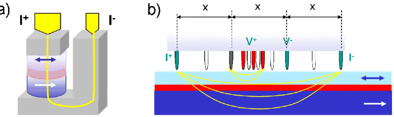
Since most of the samples we studied contain Pt layers in contact with the magnetic ones, we extensively used Hall measurements to determine their magnetic properties. These experiments were conducted on macroscopic samples, in a conventional Van der Pauw geometry presented in Figure I-6a.
Figure I-6: (a) Schematic representation of the Hall configuration. Current is injected along the x direction, Hall voltage is measured along the y direction. The magnetic field is applied along the orthogonal z direction; (b) Typical R(H) curve along the hard axis direction.
In this perfect geometrythe current is injected along the in-plane x direction and the Hall voltage is measured along the in-plane y direction. The Hall resistance is the sum of two contributions:
RH= B RO + Mz RE Equation I-3
where RH is the Hall resistivity, B the magnetic induction, and M the magnetization. R0 is the ordinary Hall coefficient related to the Lorentz force acting on moving charge carriers. RE is the extraordinary Hall coefficient associated with a break of the right–left symmetry during the spin– orbit scattering in magnetic materials and can be much larger than RO.
If the magnetic field is applied along the hard axis (Figure I-6b), the Hall resistance will first vary rapidly until the magnetization is saturated (extraordinary contribution). At larger field, the Hall resistance will vary linearly with field (ordinary contribution). The extraordinary contribution can be expressed as a function of the longitudinal resistivity as:
RE= a XX + b 2XX Equation I-4
where a and b are the skew scattering [Smi_55] and side-jump [Ber_70] coefficients.
These two scattering mechanisms responsible for the extraordinary term have their origin in the spin-orbit interaction: the classical asymmetric scattering [Smi_55] (one scattering channel is favored over the other one), which gives a linear variation with longitudinal resistivity, and the non-classical side-jump mechanism [Ber_70] (different lateral displacement for spin up and spin down electrons) which has a quadratic dependence on the resistivity. Skew scattering and side jump action of spin-orbit coupling thus cause currents of up and down electrons to deflect in
opposite directions. If the current is spin-polarized (materials with high polarization), there will be more electrons moving in one perpendicular direction than the other, resulting in an actual transverse charge current, which in addition to the Lorentz force charge separation can be detected by voltage measurements.
-15 -10 -5 0 5 10 15 -12 -8 -4 0 4 8 12 H all r e sis ta nc e ( m Oh m )
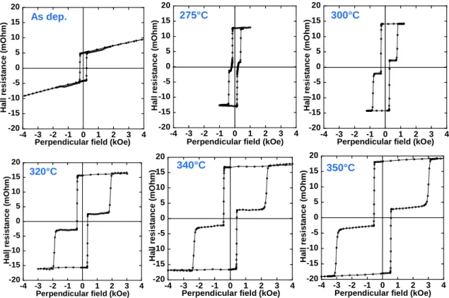
Perpendicular applied field (kOe) Ta3/Pt20/Co4.2/MgO1.4/Cu2/Pt2
c)
Figure I-7: (a) Deviation from the perfect Hall geometry between current and voltage directions and (b) Deviation of the direction of the applied field from the perpendicular direction; (c) Perpendicular Hall curve of a sample with in-plane magnetization. Deviation (a) leads to an even AMR contribution to the Hall signal. Additional deviation (b) leads to a low field AMR signal corresponding to the in-plane switching of the magnetization.
Hall effect measurements are sensitive to any deviation from the perfect orthogonality between current and voltage probes (Figure I-7a). In this case the Hall voltage will contain a contribution from the longitudinal resistivity XX. For a sample with in-plane magnetization (Figure I-7c), the total signal will be the sum of two contributions: an odd one coming from the Hall contribution, and an even one from the anisotropic magnetoresistance (AMR), which depends on the angle between magnetization and current [Tho_56]. Since magnetization progressively goes from parallel to perpendicular to the electrical current, both Hall and AMR contributions will saturate at the same field. A deconvolution of the curve allows to separate out the two contributions.
In addition, if the magnetic field is not perfectly perpendicular to the film plane (Figure I-7b), its in-plane projection will go from positive to negative. The in-plane magnetization will thus switch in a field H= HC / sinα, where HC is the in-plane coercive field and α is the angular deviation from the perfect perpendicular field orientation. This will leads to a supplementary AMR contribution (low-field negative signals in Figure I-7c).
For samples with in-plane anisotropy, a Hall measurement is equivalent to a magnetometry or a Kerr effect one. One just measures the field-induced increase of the MZ component of the magnetization up to saturation. The problem is slightly different for an out-of-plane magnetized layer. One now measures the decrease of the MZ component under the action of an in-plane field from its maximum value (saturated up or down state) down to zero where the magnetization lays in plane for a large enough in-plane field. In order to extract the effective anisotropy, the R(H) curve must be normalized, and then the MX component is extracted from the MZ variation by MX2 = 1 – MZ2. The area above the curve can thus be calculated in order to determine KEff.
Figure I-8: Effect of a small (-z) component on the magnetization curve as a function of in-plane magnetic field.
When the magnetization is in a multi-domain configuration in zero field, for a magnetic thickness close to the critical one, the MZ component will be zero whatever the applied field, and MX cannot be determined from such measurements. One must note that if the applied field is not perfectly in-plane, the measurement will also perturbed, as was the case in Figure 7b. Figure I-8 illustrates this situation. Starting from positive saturation (1), and considering a small -z component of the HX field, magnetization will switch from the +z to the -z direction (2 3) when the -z component of the applied field will be equal to the out-of-plane coercive field of the sample. In order to avoid this perturbation, experiments where always performed aligning the initial magnetization parallel to this HZ component.
The transformation from MZ to MX does not hold anymore for a structure containing more than one magnetic layer. However, as shown in Figure I-9, the successive saturation of the magnetic layers leads to a larger change of slope for Hall measurements (MZ) than for classical magnetometry ones (MX). The anisotropy fields can thus be more easily estimated.
0 0.2 0.4 0.6 0.8 1 0 0.2 0.4 0.6 0.8 1 1.2 M x/Ms 1- M z/Ms M /M s H/H sat VSM Hall 1st order anisotropy: M x H
Figure I-9: Schematic variation of the magnetization as a function of in-plane field for a structure composed of two magnetic layers with perpendicular magnetization. The blue curve is a classical VSM curve (assuming a linear field response), the red one corresponds to Hall measurements.
I-3. Thin films preparation
Cathodic sputtering is a deposition technique used for the preparation of semiconductor and metallic thin films in industry and research. This technique is interesting for magnetic thin film deposition and fabrication of tunnel junctions because of its advantages over other existing techniques like Chemical Vapor Deposition (CVD) or Molecular Beam Epitaxy (MBE) methods:
deposition ofall type of materials (metals, alloys, refractory compounds, dielectrics)
high deposition rates,
good adherence of the deposited films on the substrate,
good thickness homogeneity over large substrates (up to 300mm),
good control of layer thicknesses, down to a few tenths of nanometer.
This technique consists in the deposition on a substrate of atoms mechanically extracted from a target bombarded with accelerated argon ions of a plasma as shown in Figure I-10. The sputtering chamber is under vacuum (a few 10-8 mbar) and an inert gas is introduced to a pressure of about 10-3 mbar. Argon is the most commonly used process gas for sputtering process, since it has a high sputter yield (ionized/sputtered atoms) for most metals, is chemically inert and non-toxic, and is relatively inexpensive (compared with other rare gases as krypton or xenon). The plasma is obtained by an electrical discharge made by applying a negative voltage between target (cathode) and surrounding shield maintained at zero potential. This electrical discharge will ionize the argon atoms by collisions with the electrons. Positive ions are attracted by the target and by elastic collisions will extract atoms from the target. Atoms extracted from the target will deposit on the substrate carrying a large kinetic energy (approximately 50 to 100 times that of neutral atoms generated from thermal evaporation sources). The incoming atoms are likely to mix at the interface with the underlying layer or substrate since their energies are large enough to break bonds in most solids. This large energy is thought to be the reason for the greater adherence of layers observed for sputter-deposited films compared to thermally evaporated films.
Figure I-10: Cathodic sputtering: accelerated Ar+ ions extract atoms from the target.
After reaching the substrate surface, the pulverized atoms can diffuse and interact forming islands as a sign of thermodynamically non-equilibrium with the substrate. In this case the cohesion energy is higher between the sputtered atoms than between the sputtered atoms and the substrate surface. The growth mechanism of sputtering film is strongly influenced by several factors: chemical nature (surface energy) and crystallography of the substrate and deposited layer, interfacial energy, substrate temperature, background pressure, deposition rates.
The vacuum is very important for the film properties. In a poor vacuum (>10-7 mbar) the background pressure is mostly composed of water vapour. The water adsorbed on the surface
may increase the mobility of surface atoms and oxygen may be incorporated in the growing film. For example MgO deposited layers are very sensitive to water vapour changing its insulator or crystallographic properties.
The sputtering rate depends on the DC voltage, and can modify microstructural properties of the material. For example using high sputtering rates one can obtain polycrystalline or even more homogeneous amorphous materials, or modify the magnetic properties of magnetic materials.
Another way to increase the sputtering rates is to use permanent magnets located underneath the target. This magnetic field will concentrate the plasma near the target, thus protecting the substrate from possible heating by the plasma or inclusion of Ar atoms into the layers. This will also allow working with lower argon pressures still keeping high sputtering rates. In the case of non-metallic targets like oxides, the deposition rates are usually lowered by the accumulation of positive charges on the target. This is why in this case a radiofrequency mode is used, applying alternatively positive and negative polarization on the target in order to evacuate the positive charges. Oxide layers deposited from an oxide target are usually non stoicchiometric. As a consequence another method can be used to fabricate thin oxide layers, which consists in depositing the metallic layer and oxidizing it. There are three ways to prepare oxides from a metallic layer: reactive sputtering (sputtering the metallic layer in an argon/oxygen atmosphere), plasma oxidation (exposing the metallic layer to an oxygen plasma after deposition) and natural oxidation (exposing the metallic layer to an oxygen atmosphere for a given time after deposition). Our Actemium sputtering machine allows us to prepare layers presenting a thickness gradient. In the usual geometry, the centre of the substrate holder and the centre of the target are on the same vertical axis (Figure I-11a). In order to get rid of any plasma inhomogeneities (coming for example from the permanent magnets), the sample is rotated at 100 rpm around its axis. It is also possible to position the substrate holder off-axis (Figure I-11b) without rotation. In this case one obtains a thickness gradient on the substrate which depends on the distance d between target and sample normals. The usual geometry is when d equals 100 mm, leading to a thickness variation by a factor of about 2 on a 100 mm substrate.