HAL Id: hal-01068126
https://hal.archives-ouvertes.fr/hal-01068126
Submitted on 25 Sep 2014
HAL is a multi-disciplinary open access
archive for the deposit and dissemination of
sci-entific research documents, whether they are
pub-lished or not. The documents may come from
teaching and research institutions in France or
abroad, or from public or private research centers.
L’archive ouverte pluridisciplinaire HAL, est
destinée au dépôt et à la diffusion de documents
scientifiques de niveau recherche, publiés ou non,
émanant des établissements d’enseignement et de
recherche français ou étrangers, des laboratoires
publics ou privés.
Evaluation of the Near-Field Injection Method at
Integrated Circuit Level
Alexandre Boyer, Bertrand Vrignon, John Shepherd, Manuel Cavarroc
To cite this version:
Alexandre Boyer, Bertrand Vrignon, John Shepherd, Manuel Cavarroc. Evaluation of the Near-Field
Injection Method at Integrated Circuit Level. EMC Europe 2014, Sep 2014, Goteborg, Sweden. pp.1-6.
�hal-01068126�
Evaluation of the Near-Field Injection Method at
Integrated Circuit Level
A. Boyer
1,2, B. Vrignon
3, J. Shepherd
3, M. Cavarroc
11 CNRS, LAAS, 7 avenue du colonel Roche, F-31400 Toulouse, France, alexandre.boyer@laas.fr
2
Univ. de Toulouse, INSA, LAAS, F-31400 Toulouse, France
3 Freescale Semiconductor, Inc., Toulouse 31023, France
Abstract—Near-field injection is a promising method in order
to induce local faults in integrated circuits. This method can be used for various applications such as electromagnetic attacks on secured circuits or susceptibility investigations. This paper aims at evaluating the ability of near-field scan injection to induce local disturbances in integrated circuits. The study relies on measurements performed by on-chip voltage sensors, which provide an accurate method to characterize the induced voltage fluctuations.
Index Terms—near-field scan injection; electromagnetic attack; susceptibility
I. INTRODUCTION
Near-field injection constitutes a promising method for various applications such as electromagnetic attacks on secured circuits [1] [2] or investigations of integrated circuits (ICs) susceptibility to electromagnetic disturbances [3] [4]. The method consists in placing a miniature near-field probe in the vicinity of an electronic device and exciting the probe with a disturbance signal in order to induce a local voltage fluctuation and trigger a failure on the device under test. This method has been mainly used for analysis of IC susceptibility with injection coupled at package level. However, the injection at die level offers the advantage to locate precisely the origin of the induced faults. It can improve not only the efficiency of intentional electromagnetic injection on secured ICs such as differential fault injection (DFA) but also the diagnosis of susceptibility of an IC block.
In this paper, the ability of the near-field injection method to induce local disturbances at IC level is investigated. The proposed study aims at evaluating the possibility of the method in terms of resolution and fault generation with basic handmade magnetic and electric field probes. Moreover, it attempts to clarify the nature of the coupling between the injection probe and the circuit under test. The understanding and modeling of the coupling is essential not only to optimize the injection method, but also to understand the origins of triggered failures and the development of efficient countermeasures against intentional electromagnetic attacks.
This study is based on near-field injection measurements performed on a test chip which integrates several on-chip voltage sensors. They ensure an accurate and high frequency characterization of the voltage induced along circuit
interconnects. The first part of the paper describes the near-field injection bench and the near-near-field probes used for this study. The second part introduces the on-chip sensor and describes the test chip. The third part presents the near-field injection experimental results. Some conclusions about the injection method efficiency and the nature of the coupling between the probe and the circuit under test are provided.
II. NEAR-FIELD INJECTION TEST BENCH A. Presentation of the test bench
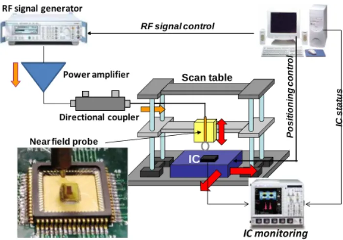
The near-field injection consists in placing a miniature near-field probe in the vicinity of a device and injecting disturbance signals in the probe in order to induce a local voltage fluctuation and trigger a failure. It relies on a near-field scan table in order to control precisely the position of the near-field probe compared to the device under test. The typical test bench is described in Fig. 1.
RF signal control P o s it io n in g c o n tr o l
Near field probe
IC IC monitoring Scan table RF signal generator Directional coupler Power amplifier IC s ta tu s
Figure 1. Near-field injection test bench
The near-field probe can be excited by various types of signal (harmonic or pulse). In this study, harmonic signals are considered for frequency analysis purpose. They are produced by a RF synthesizer followed by a 50 W power amplifier. By experience, this range of power is required to induce failures in the IC. However, one drawback of the use of harmonic signals is the major power dissipation that the probe and cables have to withstand. This constraint can be reduced with short pulse or on-off keying modulated sinus waveforms. With harmonic
signals, a directional coupler is advised to measure the amplitude of the forward power delivered by the power amplifier. As near-field probe are totally mismatched, the excitation current or voltage is not easily predictable.
The injection at IC level requires a precise control of the position of the near-field probe compared to the IC under test. For this purpose, our test bench is equipped with a laser telemeter, which has a theoretical accuracy of 12.5 µm. First, a preliminary calibration is necessary to measure the coordinates of the near-field probe in the telemeter reference frame. Then, the laser telemeter scans the IC under test and provides a 3D topology of its surface. Finally, the scan table control software is able to locate the position of the near-field probe compared to the IC under test. The scan can be done at constant height above the IC under test. Because of the noise introduced by stepper motors of the scan table, the accuracy of the positioning system is about 50 µm.
B. Near-field probes
Near-field probes are miniature and wideband antennas usually dedicated to the sense of either electric or magnetic fields in the vicinity of electronic components, printed circuit boards or antennas. They are usually based on small loops and opened tips. If they are excited by an electrical signal, they produce a strong electric or magnetic fields in their near-field region, which can couple on a device under test (DUT) to produce important voltage fluctuations locally. Near-field injection relies on probe with a good resolution and a sufficient efficiency to induce a perceptible effect on the DUT.
The development of optimized near-field probes is outside the scope of this work. In this study, two usual handmade probes made from RG405 semi-rigid coaxial cables are evaluated. Fig. 2 gives the dimensions of the probes used in this study: a tangential magnetic H and a normal electric field E probe with similar dimensions.
2.2mm Ø wire=0.45mm 2.5 mm 2.2mm Ø wire=0.45mm 3.1mm
Figure 2. Dimensions of the near-field probes: tangential magnetic field (on the left) and normal vertical electric field probes (on the right)
C. Near-field probe characterization
Near-field probe for injection are characterized by two main figures of merit: the resolution and the injection efficiency. The resolution quantifies the ability to produce an important field locally. In practice, it means that the coupling between a high resolution probe and two identical neighbor lines separated by a short distance can be distinguished. The resolution is defined as the distance that the injection probe has to travel between a first position where the coupling with the DUT is optimal and a second position where the coupling has been reduced significantly (e.g. by 3 dB for 3 dB resolution). The efficiency is the coupled voltage induced on a given DUT
for a given probe excitation. It aims at comparing the effect of different injection probe.
In order to measure the resolution and the efficiency of our injection probes, they are placed at 0.5 mm above a narrow microstrip line with a width of 0.15 mm. The probes are excited by a RF signal synthesizer which delivers 13 dBm forward power. The resolutions of both probes are similar, as shown in Table I. Fig. 3 presents the measured evolution of the voltage coupled on the microstrip line during E and H field injection. The H field probe is 15 dB more efficient than the E field probe up to 1 GHz.
TABLE I. RESOLUTION OF THE NEAR-FIELD PROBES
Resolution H field probe E field probe
1 dB 0.3 mm 0.4 mm
3 dB 0.65 mm 0.8 mm
6 dB 0.95 mm 0.95 mm
Figure 3. Comparison between measurement and simulation of the coupling of the near-field E and H probes on a microstrip line
Basic models of the near-field radiation of both probes have been constructed using elementary electric and magnetic dipole models. The evolution of the electric and magnetic fields in the vicinity of the probe can be computed. The voltages VE or
VH induced on the terminal of a line (e.g. a microstrip line) by
an electric or magnetic field probe respectively can be deduced by using the field to transmission line equations [5].
∫
+
=
Lline O line Z line L L L L Ej
C
E
h
dl
Z
Z
Z
Z
V
ω
2 1 2 1 (1)∫
+
=
Lline O line L L L Hj
H
h
dl
Z
Z
Z
V
0 tan 2 1 1ωµ
(2)From the dimensions of the tested injection probe and microstrip line, the voltage induced by the injection on the microstrip line terminal is simulated. Simulation results are superimposed on measurement curves, as shown in Fig. 3. This basic model is sufficient to obtain a good estimation of probe couplings for relatively short separation distances. The
This work is supported by the French Agence Nationale de la Recherche under contract ANR-12-INSE-005 E-Mata-Hari.
coupling increases with frequency by 20 dB/dec up to 1 or 2 GHz.
III. PRESENTATION OF THE TEST CHIP
Measuring the local voltage fluctuations in an IC induced by a near-field probe is not obvious. First, the measurement of high frequency voltage fluctuations through I/O pads and IC package introduces a non negligible attenuation and distortion. High frequency probes placed directly on IC pads disturbs the measurements and are partially coupled with the injection probe. A convenient method to measure on-chip rapid voltage fluctuation accurately, with a minimum of distortions and coupling with the injection probe relies on the use of on-chip voltage sensors (OCS) [6] [7]. A dedicated test chip with canonical structures and OCS has been developed for the characterization of near-field injection at IC level.
A. Presentation of the test chip
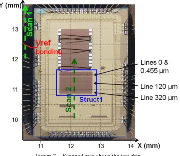
A test chip has been designed with Freescale® in 0.25 µm SMARTMOS 8 technology with 4 metal layers in order to study the near-field injection on basic interconnect and bus structures. Twenty four OCS are disseminated within the test chip to monitor local voltage fluctuations induced by the near-field injection.
The presented study is focused on one structure called Struct1, described in Fig. 4. It consists in eight 1 mm lines separated by a variable distance. The line name depends on the distance to the first one: 0 µm, 0.455 µm, 5.5 µm, 10 µm, 30
µm, 70 µm, 120 µm and 320 µm. They have a microstrip configuration: a 1.75 µm wide trace is routed on layer metal 3 over a reference plane designed in layer metal 2 and biased at a potential Vref equal to 1.25 V by a bandgap. The lines are
terminated by 50 Ω resistors. The reference voltage is connected to an external pad for test purpose. Eight OCS are placed at each line terminal to monitor the voltage fluctuations induced by the near-field probe.
Vref Vref
50 Ω Line 0 µm
Vref Vref
Line 0.455 µm
Metal 2 connected to Vref On-chip
sensors Analog pad connected to Vref Line 5.5 µm Line 10 µm 50 Ω 50 Ω 50 Ω Vref Vref Vref Vref Vref Vref 50 Ω 50 Ω 50 Ω 50 Ω 50 Ω 50 Ω Line30µm Vref Vref 50 Ω 50 Ω Line70µm Vref Vref 50 Ω 50 Ω Line120µm Vref Vref 50 Ω 50 Ω Line320µm
Figure 4. Description of Struct1
The test chip is mounted in CQFP64 package with a removable metallic lid in order to place the near-field probe as close as possible to the die surface.
B. Presentation of the on-chip sensor
In order to monitor voltage fluctuations induced by an injection near-field probe along IC interconnects, on-chip voltage sensors are disseminated within the test chip. This sensor is able to measure the waveform of voltage bounce across non accessible nodes with a precise time resolution (up to 100 ps for a development with a CMOS 0.25 µm technology). Its analog bandwidth is equal to 2.7 GHz. The acquisition principle is based on a sequential equivalent-time sampling (Fig. 5). Its principle and its implementation in the test chip are explained in [6]. In order to prevent noise coupling to sensors, they are supplied by an internal voltage regulator connected to a dedicated power supply and are isolated from the bulk substrate by a deep Nwell. Moreover the OCS is routed with only three metal layers. A complete shielding of the OCS is done with the top metal layer, avoiding the OCS to be disturbed by the radiated fields.
Reconstructed Waveform Sampling command Synchronization On-chip event Sampled data ∆Τ2 ∆Τ3 ∆Τ4 ∆Τ1 T T T T T V V
Figure 5. Principle of signal reconstruction with the on-chip sensor [6] The sensor is controlled by an external acquisition card which sends sampling clock, delay control command and converts the analog signals delivered by the sensor. The waveform of a signal can be reconstructed only if the signal is reproducible and synchronized with the sampling command of the sensor. During the near-field injection, the RF signal generator is synchronized with the OCS sampling command. Fig. 6 presents an example of reconstructed harmonic signal induced within the test chip during a near-field injection. The frequency of the probe excitation signal is 900 MHz. The step time is set to 150 ps.
IV. EXPERIMENTAL RESULTS
In this part, the measurement results obtained with the on-chip sensors are presented for injection with magnetic and electric field probes. Their performances are presented and compared. The coupling mechanisms are clarified.
A. Description of tests
Near-field scans have been performed at a constant height above lines of Struct1 with simultaneous measurement of the induced voltage fluctuations by OCS. Two scan areas have been defined and are presented in Fig. 7 by green arrows. Scan1 parses 700 µm above the Vref bonding wire in the
vicinity of I/O pads. The near-field coupling on Vref bonding
wire should induce the similar voltage fluctuation on each line of Struct1. Scan2 parses 300 µm above Struct1. If the resolutions of injection probes are accurate enough, the coupling between probes and each line of Struct1 should be distinguished.
Figure 7. Scanned area above the test chip
B. Injection with the magnetic field probe
The tangential magnetic field probe is oriented along the Y axis defined in Fig. 7 (orientation 0°) in order to optimize the magnetic coupling with Struct1 lines.
1) Evaluation of the localization/resolution
A preliminary experience consists in displacing the H field probe above the bonding wire of Vref (Scan1). The excitation
frequency is set to 1.4 GHz. The power amplifier delivers a 45 dBm forward power. Fig. 8 compares the voltage coupled only on four lines of the Struct1 for clarity purpose. The maximum induced voltage reaches up to 220 mV when the probe is placed just above the bonding wire. The same voltage is induced on the eight lines because the coupling is localized on the bonding wire Vref.
The same experiment is repeated but the probe moves along Scan2 area. Fig. 9 presents the evolution of the voltage coupled on lines 0, 0.455, 120 and 320 µm according to the magnetic field probe position. The sensors do not measure exactly the
same voltage for a given probe position. The positions of maximum coupling on these four lines are indicated by arrows on Fig. 9. They are shifted along the probe position. The maximum coupled voltage is similar for all the lines except line 0 µm. As line 0 µm is at the border of Struct1, the presence of tiling could modify its impedance and thus the coupling of the magnetic field produced by the injection probe. This result shows that the injection can be distinguished between two lines separated by more than 100 µm. At 300 µm above the IC line, the 1 dB resolution of the magnetic field probe is about 250 µm.
V
refFigure 8. Evolution of the voltage coupled on four lines of Struct1 when the magnetic field probe moves along Scan1
≈ 300 µm
Figure 9. Evolution of the voltage coupled on the four lines of Struct1 when the magnetic field probe is positionned at 300 µm above Struct1 In order to verify that the coupling is mainly magnetic, the near-field probe is rotated by 90° and the previous experiment is repeated. Fig. 10 compares the evolution of the voltage coupled on line 120 µm for both probe orientations (0° and 90°). The coupled voltage is divided by two for orientation 90° because the magnetic field direction is not perpendicular to the lines of Struct1. However, as a non negligible voltage is still measured by the sensor, the magnetic field is certainly coupled on the Vref plane placed under the lines.
Figure 10. Evolution of the voltage coupled on line 120 µm of Struct1 for two perpendicular orientations of the magnetic field probe
2) Effect of the near-field scan altitude
The effect of the near-field probe height above the die surface on the voltage coupled on the lines of Struct1is also measured. Fig. 11 presents the evolution of the voltage measured by the sensor placed on line 120 µm according to the probe height which ranges from 200 to 1000 µm. The probe is placed just above line 120 µm. Obviously, when the scan altitude is reduced, the coupled voltage increases rapidly, especially for the altitude smaller than 500 µm. At such a short distance, the coupling with the line under test is mainly due to the nearest part of the injection probe.
Figure 11. Evolution of the voltage coupled on line 120 µm of Struct1 according to the magnetic field probe altitude
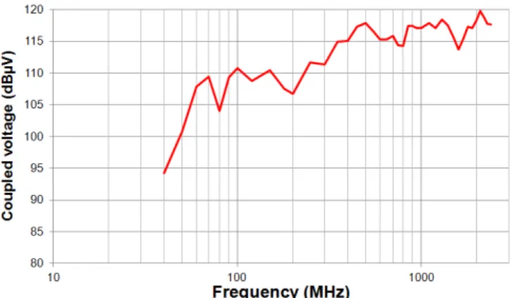
3) Frequency characterization of the magnetic field coupling
The OCS placed on line 120 µm is used to measure the evolution of the coupled voltage on the line depending on the frequency of the excitation signal of the probe. The measurements are done with a constant forward power amplitude (43 dBm measured on a 50 Ω load). Fig. 12 presents the evolution of the voltage amplitude coupled on line 120 µm depending on the frequency. This result shows that the coupling is globally improved at high frequency as expected. Voltage fluctuations of several hundreds of millivolts can be generated on a 1 mm long IC interconnect, which can be just enough to start triggering failures in digital or analog ICs.
Figure 12. Evolution of the voltage coupled on line 120 µm of Struct1 according to the magnetic field probe excitation frequency However, the coupling with the IC interconnect does not increase as continuously and rapidly as the coupling with a PCB microstrip line (Fig. 3). Moreover, the coupling is surprisingly high if the geometry of line 120 µm and the basic coupling model used in part II.C are considered. The structure of the line is certainly more complicated than a basic microstrip line. Moreover, the parasitic coupling between the line and the circuit substrate should be taken into account to model the evolution of the coupled voltage. Further measurements and simulations have to be carried at clarify the physical interaction between the injection probe and a circuit interconnect.
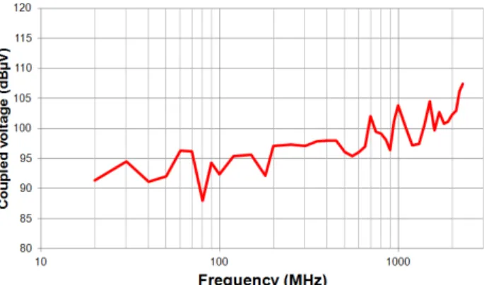
C. Injection with the electric field probe
The normal electric field probe is placed at 300 µm above Struct1 along the Scan2 area. The excitation frequency is set to 1.4 GHz. The power amplifier delivers a 45 dBm forward power. Fig. 13 presents the evolution of the voltage coupled on lines 0, 0.455, 120 and 320 µm according to the electric field probe position. The coupling between the IC lines and the electric field probe is nearly 7 times weaker than the coupling with the magnetic field probe. The measurement of the voltage fluctuation amplitude is partially disturbed by a residual noise of 5 mV. Due to the weak coupling, the four measurement curves are nearly superimposed and no conclusions about the resolutions of electric field probes can be deduced.
Figure 13. Evolution of the voltage coupled on the four lines of Struct1 when the electric field probe is positionned at 300 µm above Struct1 Fig. 14 presents the evolution of the voltage amplitude coupled on line 120 µm according to the frequency. The measurements are done with a constant forward power
amplitude (43 dBm measured on a 50 Ω load). At a given probe height, the coupling between the IC line and the electric field probe is about 7 times weaker than the coupling with the magnetic field probe. It confirms the efficiency difference between both probes measured in part II.C. The coupling increases slightly with frequency, but not as continuously and rapidly as the coupling with a PCB microstrip line (Fig. 3). Once again, this evolution can be explained by a more complicated line structure than a basic microstrip line and the complex parasitic coupling between the line and the circuit substrate.
Figure 14. Evolution of the voltage coupled on line 120 µm of Struct1 according to the electric field probe excitation frequency
V. CONCLUSION
The paper has presented a original experimental work dedicated to the evaluation of the near-field injection to induce local disturbances at IC level. This method is very promising for various applications such as electromagnetic attacks on
secured ICs or investigations of susceptibility to
electromagnetic disturbances. The measurements rely on on-chip voltage sensor to overcome the parasitic effect of IC pads and package interconnects on high frequency signal. Two handmade and basic electric and magnetic field probes have been tested. Their dimensions are in the millimeter range.
Magnetic field rpobes provide a resolution sufficient to distinguish the coupling between two lines separated by 100 µm, for a scan altitude of 300 µm. The improvement of the resolution is necessary. It can be provided by a miniaturization of the probes and a reduction of the scan altitude. It requires a test bench with a precise control of the altitude probe to prevent contact with the die surface. The measurement results have shown that even with similar dimensions the magnetic field probe produces voltage fluctuations about 7 times larger along
an IC interconnect than the electric field probe. If the magnetic field probe is connected to a RF power amplifier which can deliver several tens of watts, the amplitude of the induced voltage fluctuation can reach several hundred of millivolts. It can be enough to cause triggering failures in digital or analog circuits. The use of a harmonic RF power source has a major drawback: the heating of the injection probe. In order to increase the amplitude of IC voltage fluctuations without excessive heating of the injection probe, it is recommended to use pulsed signals.
However, the results have shown that the physical coupling between the injection probe and an IC interconnect remains complex. It has to be clarified to propose a valid model. A simple coupling model of the electric or magnetic field produced by the injection probe on a canonical line structure such as a microstrip line underestimates the actual voltage fluctuations measured on IC interconnects. Further works have to be done to improve of field coupling on IC interconnects.
ACKNOWLEDGMENT
The authors would like to thank Nicolas Mauran from LAAS-CNRS for his support on the near-field scan test bench.
REFERENCES
[1] J.M. Schmidt, M. Hutter, "Optical and EM Fault ‑Attacks on CRT‑
based RSA: Concrete Results", Austrochip 2007, 15th Austrian Workshop on Microelectronics, 11 October 2007, Graz, Austria. [2] F. Poucheret, K. Tobich, M. Lisart, L. Chusseau, B. Robisson, P.
Maurine, "Local and Direct EM Injection of Power into CMOS Integrated Circuits", 2011 Workshop on Fault Diagnosis and Tolerance in Cryptography (FDTC), 2011.
[3] A. Boyer, E. Sicard, S. Bendhia, « Characterization of the Electromagnetic Susceptibility of Integrated Circuits using a Near Field Scan », Electronic Letters, 4th January 2007, vol. 43, No 1.
[4] T. Dubois, S. Jarrix, A. Penarier, P. Nouvel, D. Gasquet, L. Chusseau, B. Azaïs, "Near-Field Electromagnetic Characterization and Perturbation of Logic Circuits", IEEE Transactions on Instrumentation and Measurement, vol. 57, no 11, November 2008.
[5] C. D. Taylor, R. S. Satterwhite, W. J. Harrison, "The response of terminated two-wire transmission line excited by a non uniform electromagnetic field", IEEE Transactions on Antennas and Propagation, vol. AP-13, pp. 987-989, 1965.
[6] S. Ben Dhia, E. Sicard, F. Caignet, “A new method for measuring signal integrity in CMOS ICs”, Microelectronic International Journal, Vol. 17, No. 1, January 2000.
[7] S. Ben Dhia, A. Boyer, B. Vrignon, M. Deobarro, T. V. Dinh, “On-Chip Noise Sensor for Integrated Circuit Susceptibility Investigations”, IEEE Transactions on Instrumentation and Measurement, vol. 61, no. 3, pp. 696-707, March 2012.

![Figure 5. Principle of signal reconstruction with the on-chip sensor [6]](https://thumb-eu.123doks.com/thumbv2/123doknet/14506272.528871/4.892.74.417.703.973/figure-principle-signal-reconstruction-chip-sensor.webp)