Development of the Recess Mounting with Monolithic Metallization
Optoelectronic Integrated Circuit Technology for Optical Clock
Distribution Applications
byERALP ATMACA
S.B. Electrical Engineering and Computer Science, Massachusetts Institute of Technology (1999) M.Eng Electrical Engineering and Computer Science, Massachusetts Institute of Technology
(2000)
Submitted to the Department of Electrical Engineering and Computer Science in partial fulfillment of the requirements for the degree of
ELECTRICAL ENGINEER in ELECTRICAL ENGINEERING MASSACHUsETTS INSTrTUTE OF TECHNOLOGY
MASSACHUSETTS INSTITUTE OF TECHNOLOGY
rFeCA 2
&07
APR 3
0
2007
Septembe 2006
LIB3RARIES
© Massachusetts Institute of Technology, 2006. All Rights Reserved.LBRRE
BARKER
A uthor ...
Department of Electrical Engineering and Computer Science ,entemhr R, 2006
C ertified by ... ...
ton G. Fonstad, Jr Vrotessor ot biectrical Engineering sor
Certified by ...
Terry P. Orlando Prmf-e-nr of MIt-trirnl U-n- ring visor
A ccepted by ... ...
mith Chairman, Department Committee on Graduate Students
Development of the Recess Mounting with Monolithic
Metallization Optoelectronic Integrated Circuit Technology
for Optical Clock Distribution Applications
byERALP ATMACA
Submitted to the Department of Electrical Engineering & Computer Science on September 8, 2006, in partial fulfillment of the
requirements for the degree of
ELECTRICAL ENGINEER
IN ELECTRICAL ENGINEERING & COMPUTER SCIENCE
Abstract
Recess mounting with monolithic metallization, or RM3 integration, is used to integrate
In0.47Ga0.53As/InP based lattice-matched high quantum efficiency p-i-n photodetectors on
silicon chips to build high performance optoelectronic integrated circuits [1]. In RM3 integration, partially processed heterostructure devices are placed in recesses formed in the dielectric layers covering the surface of an integrated circuit chip, the surface is planarized, and monolithic processing is continued to transform the heterostructures into optoelectronic devices monolithically integrated with the underlying electronic circuitry. Two different RM3
techniques have been investigated, Aligned Pillar Bonding (APB) and OptoPill Assembly (OPA). APB integrates lattice mismatched materials using aligned, selective area wafer bonding at reduced temperature (under 350'C), which protects the electronic chips from the adverse effects of high temperatures, and reduces the thermal expansion mismatch concerns. In the OPA technique, optoelectronic heterostructures are processed into circular pills of 8 pm height and 45 pm diameter, the pills are released
from the substrate, and collected through a process that involves decanting. The pills are then assembled into recesses on silicon chips using manual pick & place techniques, and they are bonded to the metal pads on the bottom surface of the recesses using a Cu-AuSn solder bond. A new magnet assisted bonding technique is utilized to obtain clamping pressure to form the solder bond. The gap between the pill and the surrounding recess is filled using BCB, which also provides good surface planarization.
Contents
1
Introduction 111.1 Electrical and Optical Interconnects ... 12
1.2 Optoelectronic VLSI Technologies ... 15
1.2.1 Monolithic Optoelectronic Integration ... 16
1.2.1.1 Common Epi-layers ... 18
1.2.1.2 Epitaxy-on-Electronics ... 18
1.2.2 Hybrid Optoelectronic Integration ... 19
1.2.2.1 Wire Bonding ... 20
1.2.2.2 Flip-chip Bonding ... 20
1.2.2.3 W afer Fusion ... 23
1.3 Recess Mounting with Monolithic Metallization ... 24
1.4 Thesis Organization ... 26
2 Analysis of 1550 nm InO.47Gao.53As/InP based p-i-n Photodetectors for RM3 Applications 29 2.1 Review of Conventional Clock Distribution on ICs ... 29
2.1.1 Optical Clock Distribution ... 31
2.2 Analysis of 1550 nm Ino.4 7Ga0.53As/InP based p-i-n Photodetectors 33 2.2.1 Semiconductor Physics for Heterostructures ... 36
2.2.2 Electrical Mobility Model for InGaAs/InP Material System 38 2.2.3 Carrier Recombination Models ... 39
2.2.4 Analysis of Reverse Biased p-i-n Photodiode ... 41
2.2.4.1 DC Photocurrent ... 41
2.2.4.2 Frequency Response ... 42
2.2.5 ATLAS Two-Dimensional Device Simulations ... 47
2.2.5.1 Physical Definition of the Heterostructure ... 47
2.2.5.2 Electrical Characterization ... 50
2.2.5.3 Optical Characterization ... 51
3 Recess Mounting with Monolithic Metallization Technology Development 57
3.1 A ligned Pillar Bonding ... 58
3.1.1 Reactive Ion Etching of InP Based Materials ... 59
3.1.1.1 SiO2 Etch Mask for InP Etching ... 60
3.1.1.2 CH4-H2 Plasma Etching of InGaAs/InP ... 62
3.1.2 Metal Deposition on InP Pillars ... 65
3.1.3 Recess Preparation via Dry Etching on CMOS chips 66 3.1.4 Metal Assisted Bonding for RM3 ... . . . 71
3.1.4.1 RDA M8 Flip-Chip Bonder ... 71
3.1.4.2 Palladium-to-Semiconductor Bond ... 72
3.1.4.3 AuSn Eutectic Solder Alloy Bond ... 75
3.1.5 APB InP Substrate Removal ... 79
3.1.6 Summary of APB Results and Process Limitations ... 82
3.2 OptoPill A ssem bly ... 86
3.2.1 OptoPill Fabrication ... 86
3.2.1.1 Fabrication of OptoPillars ... 87
3.2.1.2 OPA InP Substrate Removal ... 89
3.2.1.3 Collection of OptoPills in Clear Methanol Solution 91 3.2.2 Micro-Scale Pick-and-Place (MPAP) Assembly Technique 92 3.2.3 Magnet Assisted Bonding ... 94
3.2.3.1 Estimation of the Magneto-Static Clamping Pressure 98 3.2.4 OPA Post-Fill Processing ... 106
3.2.4.1 Ohmic Contact Formation on the OptoPill ... 106
3.2.4.2 Gap Filling and Planarization using BCB ... 110
3.2.4.3 Other Post-Fill Processes ... 112
3.2.5 Summary of OPA Results ... 112
3.3 Summary of the RM3 Process Development ... 114
4 Summary and Conclusion 117 4.1 Directions for Future Research ... 119
List of Figures
1-1 The Epitaxy-on-Electronics process flow ... 19
1-2 A wire-bonded optoelectronic device ... 20
1-3 Illustration and SEM image of a coplanar bonded VCSEL on an IC ... 22
1-4 Illustration and SEM image of a top-bottom bonded VCSEL on an IC ... 22
1-5 Illustration and SEM image of top-contact bonded VCSEL on an IC ... 23
1-6 OEIC fabricated by Recess Mounting with Monolithic Metallization ... 25
2-1 General approaches for optical clock distribution ... 32
2-2 The growth cross-section of the InGaAs/InP p-i-n photodiode ... 35
2-3 Velocity-field characteristics for carriers in the InGaAs/InP material system 39 2-4 Carrier transit time effects on bandwidth ... 44
2-5 Equivalent circuit of a p-i-n photodiode ... 45
2-6 Bandwidth as a function of the load resistance ... 46
2-7 The ATLAS mesh structure of the p-i-n photodiode ... 47
2-8 Energy band diagram of a pn heterojunction ... 49
2-9 Thermal equilibrium energy band diagram of the photodetector ... 49
2-10 Energy band diagram of the photodetector under 1V reverse bias ... 50
2-11 Current-voltage characteristics of the photodiode ... 51
2-12 DC photocurrent of the photodiode ... 52
2-12 Optical frequency response of the photodiode ... 53
2-13 Optical transient response of the photodiode ... 54
3-1 The Aligned Pillar Bonding process flow ... 59
3-2 APB process flow for InGaAs/InP pillar fabrication ... 63
3-3 SEM of ECR-RIE etched InGaAs/InP pillars ... 64
3-4 SEM of a CMOS recess after an attempt to clean it by wet etching ... 67
3-5 SEM and EDS analysis of the CMOS recess ... 69
3-6 Metal pad exposed on the bottom of a CMOS recess ... 70
3-8 Gold-tin equilibrium phase diagram ... 76
3-9 Under-cutting problem during InP substrate removal ... 80
3-10 Epoxy flow under vacuum to prevent the air bubbles ... 81
3-11 InP detectors transferred into recesses on a CMOS chip using APB technique 81 3-12 Ohmic contact formation on the InP pillars bonded on a CMOS chip 82 3-13 SEM of an InP photodetector and the Au ohmic ring in a CMOS recess 83 3-14 Sidewall SEM of InP pillars transferred on a CMOS chip ... 84
3-15 AuSn alloy on top of the InP pillar after an unsuccessful attempt of bonding 85 3-16 OptoPill Assembly process flow ... 86
3-17 Illustration of the OptoPillar definition process ... 88
3-18 InP substrate removal in OPA ... 90
3-19 OptoPill collection inside a test tube ... 91
3-20 Illustration of OptoPills dispensed on a silicon substrate for MPAP ... 93
3-21 SEM s showing OptoPills ... 94
3-22 The chip and the magnet during the Magnet Assisted Bonding ... 96
3-23 Typical m agnetic hysteresis loop ... 97
3-24 Magnetic hysteresis loop of 0.38 pm Ni film deposited on a GaAs substrate 98 3-25 Problem geometry for 2D magneto-static simulations ... 100
3-26 The magnitude of the magnetic flux density around the CoSm magnet 101 3-27 Clamping pressure vs. horizontal distance from the center of the magnet 102 3-28 Clamping pressure vs. distance from the magnet ... 103
3-29 Problem geometry with 2 nickel layers ... 104
3-30 Clamping pressure vs. horizontal distance with 2 nickel layers ... 105
3-31 Metal ring formed on the surface of a bonded OptoPill ... 107
3-32 SEM of CMOS recess after the bonded pill comes out ... 108
3-33 Magnetization of nickel as a function of temperature ... 109
3-34 Process flow for gap filling and planarization with BCB ... 110
3-35 SEMs demonstrating the gap filling and planarization with BCB ... 111
3-36 Illustration of the optoelectronic device definition by groove-etching 112 4-1 The growth cross-section of a resistive pill structure ... 121
List of Tables
1-1 Material parameters of important semiconductors and dielectrics ... 17
2-1 Electrical mobility model parameters for the InGaAs/InP material system 39
2-2 SRH recombination parameters for the InGaAs/InP material system 40
2-3 Direct and Auger recombination parameters for the InGaAs/InP material system 40
3-1 Room temperature mechanical properties of 80 wt.% Au -20 wt.% Sn alloy 76 3-2 Magnetic B-H data used in the magneto-static simulations ... 100
Chapter 1
Introduction
As the integrated circuit technology is being driven beyond the VLSI regime, transistor performance and integration density are no longer the primary limitations on the performance of digital systems. Rather, the electrical wires that interconnect the transistors within electronic systems determine the performance. Electrical interconnect limitations arise from the finite resistance, capacitance and inductance of the electrical conductors. For example, the electrical bus lines that carry data between chips on a multi-chip module (MCM) have to be operated at clock frequencies much lower than the on-chip clock rate due to the parasitics associated with the long metallic wires. As the clock frequencies are moving into the gigahertz regime, the on-chip global interconnects are also becoming very difficult to implement for similar reasons.
The electrical interconnect problems were first observed in long-distance communication systems in 1960s. After the invention of the semiconductor laser and the development of optical fibers, optical communication links that offer higher bandwidth and lower loss than electrical interconnects have become the backbone of long-distance communication channels replacing the electrical coaxial cables and copper wires. As it once revolutionized the long-distance communications, the use of optics can now offer solutions for several electrical interconnect performance limitations at shorter length scales that include the on-chip, chip-to-chip and board-to-board scales. In Section 1.1,
some of the motivations for the use of optical interconnects in digital systems are reviewed.
Unlike long-distance communication links where a single optical fiber, a discrete laser, a discrete photodetector, and separate driver and receiver electronics are well suited to the task, optics will be successful at small size scales only if the optical interconnect, the optical emitter and detector, and the electronics can be constructed together, i.e. integrated. Therefore, a key technology needed to realize such optical interconnects is the means of fabricating optoelectronic integrated circuits (OEICs), which closely couple VLSI-complexity electronics with large numbers of optoelectronic devices such as semiconductor lasers, light emitting diodes (LEDs), optical modulators and photodetectors. The central theme of this thesis is the development of an optoelectronic integration technology that is termed Recess Mounting with Monolithic Metallization (RM3). Section 1.2 surveys various optoelectronic integration techniques to understand the advantages and limitations of the OEICs made with RM3 technologies in the context
of optical interconnect system performance.
1.1
Electrical and Optical Interconnects
Low power dissipation, small latency, small physical size, and the ability to integrate with mainstream silicon electronics in large numbers are all required of optoelectronic devices for dense optical interconnects at the chip-to-chip and on-chip levels. To start the discussion of the benefits of optical interconnects to electronic chips in digital systems, it is important to understand some of the physical limitations to the scaling of electrical interconnections.
Conventional electrical interconnects possess resistance and capacitance, which determine the rise time of the signals. The finite rise times limit the rate at which the signals can be sent down the wire. If the bits are sent too close in time, they will overlap because of this finite rise time. An important issue here is that the rise times do not scale with the shrinking size of the electrical interconnects in VLSI systems [2]. The shrinkage of an electrical line in all dimensions by some factor makes no change in the RC time
constant of the line, and the lines cannot keep up with the transistors, which get faster as the feature sizes get smaller.
A similar problem arises for the longer inductive-capacitive (LC) lines such as the
electrical interconnects at the chip-to-chip and board-to-board levels. The rise times on such lines are limited by skin-effect resistance, which becomes worse at high frequencies. The form of the rise time has a much longer tail for LC lines than the RC case, leading to worse problems with overlapping of successive bits. This particular form of tail arises from the frequency dependence of the effective resistance that results from the skin effect. For high-speed systems nearly all lines other than on-chip lines are LC lines. There is a drop by as much as a factor of 10 in the number of bits per second that can be transmitted by an LC line compared with an RC line for a certain interconnect cross-sectional area. Hence, the bandwidth limitation is a more urgent problem for off-chip electrical interconnects [3].
Optical interconnects do not suffer from this aspect ratio limit. The physics of loss and signal distortion in optical interconnection is completely different. Loss in optical media is essentially independent of the modulation bit rate, even into the terahertz regime. Optical attenuation can be relatively very small; it is negligible in free-space propagation over scales of meters, and in optical fibers over kilometers (e.g., 0.2 dB/km loss at 1550 nm wavelength). Optical systems readily exceed the electrical scaling limit derived here by multiple orders of magnitude. For example, a single-mode optical fiber, 125 tm in diameter and 15 km in length, would have only 3 dB of distance dependent loss. Sending signals at, for example, 100 Mb/s is simple and routine in such a system. A simple electrical interconnect with the same length and cross section would, according to the scaling analysis of this paper, be able to carry less than 0.1 bit/s of data [3]. More sophisticated optical systems can handle much greater distances and bit rates, with 160 Gb/s transmitted over 232 km of optical fiber.
The distance-dependent loss and distortion in an optically interconnected digital system is much easier to model and take into account. An optical interconnect can be taken over any distance in a digital electronic system without degradation. On the other hand, with electrical interconnects, connecting over any substantial distance is
increasingly difficult. Hence with optics, it is possible to take architectures and continue to scale them to higher clock speeds without having to deal with the problem of aspect ratio.
The cross-sectional area of an electrical interconnect largely determines its performance, and the aspect ratio limit constrains the maximum interconnect density that can be achieved with electrical interconnects. Fiber optical interconnects have an important advantage in this regard. Optical fibers are very compact (typical fiber outer diameter is 125 pm) and flexible and may be densely packed in one- and two-dimensional arrays. Fiber optic connectors are also more compact than electrical connectors, thus providing another advantage in density. Another aspect of optical interconnections that lead to a higher density is the ability to intersect optical paths. For example, in planar lightwave circuits, waveguides may intersect orthogonally without cross-talk. In free-space optics, where a transmission medium is not required, optical paths can be crossed arbitrarily.
The delay on optical signal or clock paths is not strongly dependent on temperature, and signal edges do not degrade substantially over tens of meters. By contrast, the effective delay in electrical lines depends on the temperature because the resistivity of metal depends on temperature. The rise time on electrical lines is proportional to resistance of the line, and the signal delay on RC lines is proportional to the resistance. In addition, gate delay varies with fabrication and temperature. In the case of optics, the propagation delay due to the finite velocity of light can still not be avoided, but the arrival time of optical signals is likely to be reliable and predictable.
There is also variability in delay from the driver and receiver circuits in both the electrical and optical cases. With the use of small optoelectronic devices integrated well with their electrical drive circuits, the optical circuits should have the same or fewer numbers of stages than their electrical counterparts, and hence comparable or better delay variation.
In general, in optics, the power consumption does not depend on the distance of signal propagation. By contrast, the power required to distribute signals or clocks with electrical interconnects will depend on the total length of the distribution lines. Optics
could eliminate the need for high-power clock driver circuits on chips. Telecommunication receivers, which are usually designed with large input capacitance and minimum detectable power, are too large and consume too much power for use in optical interconnections. With integration of relatively small photodetectors, relatively low power dissipation and small size are possible in optical interconnect receiver circuits. Optical output devices, such as quantum well modulators and Vertical Cavity Surface Emitting Lasers (VCSELs), must operate at relatively low power so that the transmitter circuits do not dissipate too much power. With quantum well modulators, total power dissipation in the range of a few milliwatts is also possible for transmitter circuits [4].
Conventional electrical interconnects suffer from mutual electromagnetic coupling effects. These effects become more severe as the signal bandwidth increases since the mutual coupling is proportional to the signal frequency. Photons do not generate stray electric and magnetic fields. With proper design, optical interconnects can offer communication links with extremely low cross-talk.
In conclusion, optics is a promising technology for high-density, high-speed interconnects typically required in modem computation and communication systems. However, the realization of optical interconnects can only be possible with high-density, high-speed and low-power optoelectronic integrated circuits.
1.2
Optoelectronic VLSI Technologies
The development of optoelectronic integrated circuits (OEICs) that combine large numbers of optoelectronic devices with VLSI-complexity electronics is the key technological challenge associated with the implementation of optical interconnects. The choice of specific optoelectronic and electronic devices to combine the high transmission bandwidth of optical signals and the information processing capacity of electronic circuits is the central theme in the development of an optoelectronic integration technology. Fundamental incompatibilities between the III-V compound semiconductors that are commonly used for optoelectronic devices (GaAs, InP, etc.), and silicon, the dominant electronic semiconductor material, have been an obstacle in the realization of OEICs. These incompatibility issues have resulted in the development of a number of
different optoelectronic integration technologies that can be broadly categorized as either monolithic or hybrid.
1.2.1 Monolithic Optoelectronic Integration
In the monolithic approach the optics and electronics are inherently proximal. The close proximity aspect of the monolithic optoelectronic integration can reduce the parasitics associated with contacts and interconnects, thus improving the performance of the optoelectronic circuits. The power dissipation of the optoelectronic circuit is also reduced since integrating all systems on the same chip eliminates the need for buffer electronics that drive off-chip output signals. In most applications, the production cost can also be reduced since the monolithic integration enables the easy packaging of the optoelectronic circuits [5].
Monolithic integration employs a common semiconductor substrate on which both electrical and optical devices are formed. Monolithic integration has proven difficult due to fundamental material incompatibilities as mentioned before. For example, VLSI complexity electronic circuits are often fabricated from silicon, which is a poor light emitter due to its indirect bandgap. On the other hand, semiconductor optical sources and detectors can readily be made from III-V compound semiconductors such as indium phosphide (InP) and gallium arsenide (GaAs) that are direct bandgap and have much better optical emission properties. The problem is that these two materials systems (silicon and the III-V's) are quite different and thus are difficult to integrate on the same chip. The lattice mismatch between different semiconductor materials can cause dislocations that often introduce deep-levels, which degrade the device performance. The dimensional change due to the heterogeneous thermal expansion not only induces large stress on a microscopic scale, but also makes it impossible to maintain macroscopic alignment of patterns. Coefficients of thermal expansion (CTE) and lattice constants of some of the materials used in this research are shown in Table 1-1.
Table 1-1: Material parameters of important semiconductors and dielectrics
Parameter Si GaAs InP InO.53Gao.47As SiO2
Lattice constant (A') 5.43095 5.65330 5.86860 5.86860 N/A CTE (x 10- C4) 2.60 6.86 4.75 5.67 0.50
The recent progress in compound semiconductor VLSI fabrication has made it possible to build very high speed GaAs and InP based optical transmitter and receiver circuits. The availability of both electronic circuits and optoelectronic components such as lasers, LEDs and detectors in InP and GaAs based material systems is an important achievement towards the full monolithic integration of optoelectronic systems. However, the processing constraints of optoelectronic devices are typically inconsistent with standard VLSI fabrication even when the same kind of substrate is used to fabricate both the electronic circuits and the optoelectronic devices. For example, the optimum conditions demanded by the high quality epitaxial growth are often not compatible with the processing requirements of electronics. GaAs VLSI circuits using aluminum based metal interconnections cannot sustain any elongated processing at temperatures above 4700C [6].
For silicon-based electronics, thermal cycle above 550'C is also detrimental due to dopant diffusion and the degradation of ohmic contacts and metallization layers [7].
On the other hand, the temperatures required for optimal growth can be as high as 5500
C-600'C for InP and 600OC-7000C for GaAs, and it is generally very difficult to grow high quality epitaxial layers on pre-processed electronic circuits without degrading the functionality of the electronic circuit [8].
Most commercial optoelectronic applications rely on hybrid integration, but there is considerable research effort to develop monolithic optoelectronic integration techniques because of the higher performance, lower packaging cost and lower power dissipation of monolithic OEICs. There are a number of approaches to monolithic optoelectronic integration.
1.2.1.1 Common epi-layers
In this technique, both the optical and the electrical devices are fabricated in the same epitaxial layers. For example, since HBT and laser diode heterostructures are similar, selected areas of the wafer can be processed into HBTs and other areas into laser diodes. Unfortunately, this approach does not allow for the independent optimization of both optical and electronic devices. In addition, poor planarity and electronic device uniformity restrict this technique to small to medium scale integration [8].
Alternatively, the optical and electrical device epitaxial heterostructures can be separated to avoid compromising optical and electrical device performance. Optical device layers, which are typically quite thick (3-8 pim), can be grown beneath the electrical device layers, which are typically thin (~I pm), and this allows the independent optimization of the electrical and optical devices. A thin layer of material is removed to gain access to the thick layers in the lateral areas where optical devices are to be formed. The improved surface planarity of this process also allows the use of monolithic processing to complete the fabrication of the devices after the epitaxial growth is done. One drawback of this approach is that the electronic devices do not take advantage of the commercial electronics infrastructure [8].
1.2.1.2 Epitaxy-on-Electronics (EoE)
Epitaxy-on-Electronics is based on epitaxially growing the optoelectronic device layers on the host substrate of electronics, which are typically 111-V compound semiconductors, in recesses opened down to the underlying wafer surface [8]. Removing the polycrystalline material, which is deposited on the surface of the chip during the epitaxy, leaves behind photonic epitaxial islands intermixed with the electronic devices. After the removal of the polycrystalline material, the top surface of the electronic chip is highly planar, and monolithic processing can be used to finish the optoelectronic device fabrication, and to interconnect with the pre-existing electronics on the chip. The EoE process is illustrated in Figure 1-1.
MonoliUthically integrated
1pitxia heerosruture surface emitting diode
GaAs MISFIT circuitry with E pitamal tteerostructure sCSEL or LED) Emission
muld-laver interconnects
Dielectric a mls
growth well
N+e fo mimpbntn Senim-rsutabng
1;aAS~~a~ Waerbafer Cntc GaAs vw afer
a. Processed GaAs IC wafer as b. After epitaxy and c. Optoelectronic device received from the manufacturer prior to removal of the processing and
polycrystalline deposit integration completed
Figure 1-1: The Epitaxy-on-Electronics Process: a) Dielectric growth wells are opened
on the back-end of the GaAs wafer, b) optoelectronic device epitaxy and the removal of the polycrystalline deposit from the surface of the chip, and c) after completing device processing and integration
The difficulty of obtaining very clean surfaces, required for high quality epitaxial growth, on the bottom of the dielectric growth window is an important limitation of Epitaxy-on-Electronics. The substrates used for electronic circuits are not as high quality as those used for optoelectronic devices, the ion implantation needed to form the back contact area introduces damage, and the growth surface can easily be damaged by the etch processes employed during the opening of the dielectric windows. Furthermore, Epitaxy-on-Electronics is restricted to GaAs and InP integrated circuits, and it is not suitable for
CMOS chips due to lattice mismatch and heterogeneous thermal expansion when the
electronic substrate used is silicon. EoE is also limited by degradation of the electronic circuits at elevated temperature, which limits the epitaxy temperature to under 500'C. These limitations of the EoE technology make it necessary to consider other RM3 processes that do not require growing optoelectronic epitaxial layers on electronic substrates.
1.2.2 Hybrid Optoelectronic Integration
Monolithic integration offers a reduction in cost, an increase in functionality and an improvement in performance over hybrid circuits, but due to the limitations of the monolithic integration technologies described so far, most commercial optoelectronic
systems rely on hybrid integration. In the hybrid approach, the optics and the electronics are formed separately but are then packaged in close proximity. Hybrid integration brings together separately optimized optoelectronic and electronic parts through a variety of techniques such as wafer bonding, wire bonding and flip-chip bonding.
1.2.2.1
Wire bonding
The wire bonding technique involves the bonding of gold or aluminum wires between contact pads on different chips or assembly boards [10]. Die on the carrier or the substrate are moved through a wire bonder, and each bond is individually produced. The machine's pattern recognition system identifies the die, transforms and corrects the taught locations for each bond, and individually moves to each location to produce an interconnection. This makes wire bonding a costly operation for large-scale integration. For high frequency applications, this technique is also limited by the wire bond inductance. It may be possible to use the wire bond inductance to build noise-matching or inductive-peaking networks to improve the performance of the optoelectronic circuit, but this is more the exception than the rule, and lead inductance is in general a major limitation. An illustration of a wire-bonded optoelectronic device is shown in Figure 1-2.
VLSI Chip
PCs
Photonic Devices
Figure 1-2: An illustration of a wire-bonded optoelectronic device
1.2.2.2
Flip-chip bonding
Currently, flip-chip bonding is the most mature technology for the combination of III-V optoelectronics with silicon integrated circuits. Like most other hybrid integration techniques, it allows the independent optimization of electronics and optoelectronic
devices. The basic technique of flip-chip bonding has been used for over thirty years as an alternative to the wire bonding of integrated circuits. In the basic flip-chip bonding technique, solder balls are applied to the IC bondpads, and the chip is brought into rough alignment with a package. The solder is then reflowed by heating, and the IC and package are pulled into proper alignment by the surface tension of the molten solder. The flip-chip bonding technique is preferred over wire bonding because of the reduced parasitics and a shorter assembly time [9-11].
While this basic technique is very well suited to the packaging of electronic die, two significant modifications have been made in applying it to OEIC fabrication. First, unlike conventional flip-chip packaging, the substrates of the optoelectronic die which are flip-chip bonded to form OEICs are typically removed, leaving individual free-standing devices. This is done in order to address the issues arising from the large thermal expansion mismatch between silicon and compound semiconductors. Second, suitable bondpads must be prepared on the optoelectronic sample. Common optoelectronic devices are highly non-planar. Producing contacts to both sides of the optoelectronic device is a challenging fabrication task, particularly given the high device densities that are desired and the bondpad co-planarity required for successful flip-chip bonding. Recently, three different techniques have been reported that address the co-planarization problem in the flip-chip optoelectronic integration process [12].
In the first technique, optoelectronic devices are fully processed before bonding, and the n- and p-contacts are formed in such a way that they are on the same plane as illustrated in Figure 1-3. In order to accomplish this, Au is electroplated on the n-contact to a height that is level with the p-contact. In addition to this, 5 ptm of Au is deposited onto both the electroplated Au post and the p-contact. On the IC chip, Ti-Au-InSn is deposited onto the Al bonding pads. The bonding is done at 180'C, which melts the InSn contacts and bonds the two chips together. It is believed that the alloying of InSn with Au occurs during the bonding phase. After the bonding, the optoelectronic substrate is removed, leaving individual optoelectronic devices locally bonded to pads on the electronic chips.
hv Sbiae nvd A sec stop lay= n-sDirror 500 Insm. I OW A Au,
Figure 1-3: Illustration (left) and SEM (right) image of a coplanar bonded VCSEL on an
electronic chip [12]
Electroplating for co-planarization of the solder bonds can be avoided by depositing Au posts onto pads on the electronic chip to the approximate height of the optoelectronic device in order to form part of the top contacts as can be seen in Figure 1-4. After the bonding, epoxy is flowed between the two chips, the optoelectronic substrate is removed, and the n-contact of the optoelectronic device and the metal trace between the n-contact and Au posts are deposited and annealed. Step coverage is not a serious problem since the epoxy provides a bridge between the optoelectronic device and the Au post.
Su-uaw hVnnpctmat
a-m rrorPixC1 Chip
Active I GaA1,As confined to 5000A in~n, IWO A A Bon To 00 A Ti, Contact Conta
Figure 1-4: Illustration (left) and SEM image (right) of a top-bottom bonded VCSEL on
an electronic chip [12]
Both of the methods described so far use tall metallic posts to achieve a level of co-planarity for generating electrical contacts to both sides of the optoelectronic device. The Au posts are usually electroplated and the height variations cannot be avoided. Beyond this, the electrical parasitics associated with these posts can limit the performance of the OEICs at high frequencies. The use of metallic bonding posts is
eliminated in a third technique by attaching the optoelectronic wafer to the electronic chip by the help of an epoxy. After the attachment, the optoelectronic wafer substrate is removed and the remaining epitaxial layers are processed into optoelectronic devices as illustrated in Figure 1-5. The contacts are made to each side of the optoelectronic device, and polyimide is spun on and patterned to provide an insulating layer. Au is then deposited and patterned into traces that connect the p- and n-contacts to their corresponding bondpads on the electronic chips. However, the yield in this process is very low, and the non-planar top surface of the integrated complete OEIC prevents the fabrication of dielectric waveguides on top of the chip.
Substzmtc
Figure 1-5: Illustration (left) and SEM image (right) of a top-contact bonded VCSEL on
an electronic chip [12]
1.2.2.3
Wafer Fusion
In wafer fusion bonding, the surfaces of two mirror-polished wafers are prepared for the bonding process, and then brought into contact for bonding at room temperature in a
sufficiently clean environment in order to avoid particles between the wafers. Directly
after room temperature bonding, Van der Waals interactions or hydrogen bridge bonds
determine the adhesion between the two wafers. Higher bond energy, required for most practical applications, may be obtained by an appropriate heating step [13]. For compound semiconductor bonding, at temperatures as high as 1100'C, the Group III atoms diffuse along the two surfaces, and when the materials are cooled, they form the original compounds with the Group V elements on the other side of the interface resulting in a very strong covalent bond [14]. Lattice matching is not an issue for wafer bonding, but stress due to thermal expansion coefficient mismatch can lead to deformation of bonded wafers. Higher temperatures required for the covalent bonding can result in dopant diffusion and the degradation of ohmic contacts and the metallization layers; hence the two wafers must be fused together before the fabrication of the electronic circuits, requiring the development of a new VLSI technology. Therefore, wafer fusion is not a cost-effective way of building an optoelectronic integrated circuit technology.
1.3
Recess Mounting with Monolithic Metallization
The Recess Mounting with Monolithic Metallization (RM3) technology
overcomes most of the limitations of the flip-chip bonding techniques mentioned so far
by bonding the individual optoelectronic devices into recess openings on the silicon
integrated circuits. Modem integrated circuits have several layers of metallization, and in the RM3
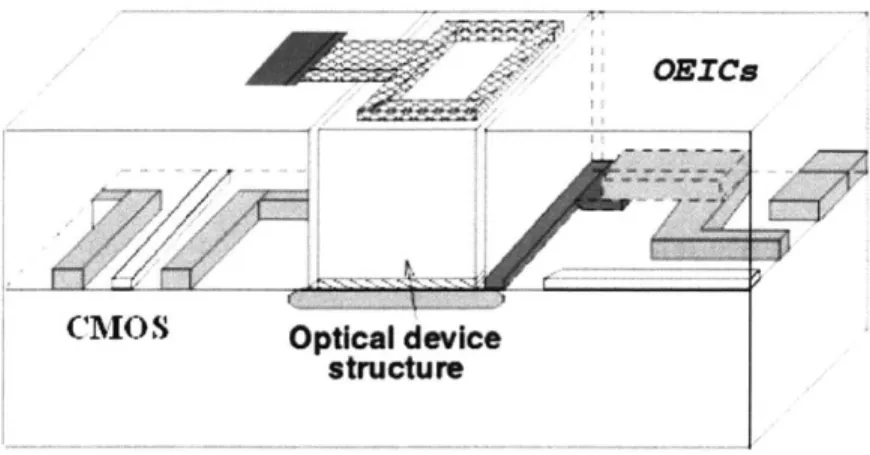
process, the top and bottom contacts of the optoelectronic devices can be made at different levels of IC metallization since the optoelectronic device mesas are placed into recesses etched in the dielectric back-ends of the electronic chips. This allows the use of vertical optoelectronic devices and avoids the tedious manufacturing process flow for making contacts to both sides of the optoelectronic device. In addition, it reduces the parasitics associated with the Au posts that are used for co-planarization before the bonding of the devices can take place. An illustration of an recess mounted optoelectronic device is shown in Figure 1-6.
OBICS
/ 7f
CMOS Optical device
structure
Figure 1-6: Illustration of an OEIC fabricated by Recess Mounting with Monolithic
Metallization (RM3) process
RM3 allows the use of compound semiconductor based optoelectronic devices
such as lasers and photodetectors on silicon chips. Although it is possible to make some of these optoelectronic devices, such as photodetectors, from silicon processes, the performance of the InP and GaAs based photodetectors are much better than the performance of silicon based photodetectors. In Chapter 2, it will be shown the performance of high-speed optical clock distribution can be significantly improved by using InGaAs/InP based photodetectors instead of integrated silicon photodetectors.
The major advantage of RM3 over the flip-chip bonding technique illustrated in
Figure 1-5 is the planar surface obtained by the RM3 process. Both processes use metal
traces to form the electrical interconnect to the top terminal of the device, and the bottom interconnect is fabricated using a larger pad. Therefore, the interconnect parasitics are comparable. However, the approach in Figure 1-5 results in a highly non-planar surface, and no further processing can be done on the wafer after the bonding of the optoelectronic device. In RM3, the planar surface achieved after the integration allows the
continuation of monolithic processing that can be used to fabricate integrated optical waveguides on the top surface of the chip to distribute the light signals.
In conclusion, RM3 is a modified flip-chip bonding technique, which has
advantages over the conventional optoelectronic flip-chip bonding techniques described in this section. Among these advantages are a simplified process flow, very good
planarization that leads to reduced top contact parasitics and lower packaging costs. In addition, the planar top surface of the OEICs fabricated by the RM3 processes is very suitable for making integrated optical waveguides on top of the electronic chips.
1.4
Thesis Organization
The main concern of this thesis is the processing technology development for the Recess Mounting with Monolithic Metallization optoelectronic integration technology to integrate InP based heterostructures on silicon chips. Besides being a key component in the development of optical interconnects, an optoelectronic integration technology can also find applications in sensor arrays, wireless infrared local area networks and fiber-optical communications. In this thesis, the emphasis is on the development of the RM3 optoelectronic integration technology to build optical interconnects. More specifically, the RM3 concept is used for studying the integration of indium phosphide based lattice-matched photodetectors at 1550 nm wavelength with silicon chips for optical clock distribution applications. The issues regarding the conventional electrical clock distribution in modern digital CMOS chips are reviewed in Chapter 2, and the advantages offered by using an RM3 process for optical distribution of the clock signals across a chip
is examined. Chapter 2 includes a detailed analysis of the physics and operation of the p-i-n photodiode used in the integration work. This discussion includes the effect of using heterojunctions in the device layers, the derivation of the current voltage characteristics, responsivity, quantum efficiency and the frequency response. Two dimensional device simulations of the InGaAs/InP based p-i-n photodetectors are used to support the analysis of the photodetector.
Chapter 3 is the main chapter of the thesis, and it focuses on the technology development for the RM3 process. RM3 technology is an "exotic" process, and a series of
new processing technologies were developed for the RM3. Two major RM3 processes
researched in this thesis are the Aligned Pillar Bonding and OptoPill Assembly. Aligned Pillar Bonding is derived from the conventional flip-chip bonding techniques, and it utilizes an RDA M8 Flip-Chip Bonder instrument. OptoPill Assembly is based on manual assembly of OptoPills of p-i-n heterostructures on recesses opened on silicon chips. A
new solder bonding method using magnetic interaction forces is developed. Magneto-static simulations are used to quantitatively analyze this technique. Bonding experiments were carried out with the help of Mindy Teo [39c].
Chapter 2
Analysis of 1550 nm 1nO.
47
GaO.
3
As/InP
based p-i-n Photodetectors for RM
3
Applications
RM3 integration techniques can be utilized in numerous optoelectronic applications including optical interconnects for on-chip and chip-to-chip clock and data distribution. This chapter starts with a discussion of the motivations for on-chip optical clock distribution, and it reviews the problems with the present clock distribution schemes. It then highlights how RM3 can be used to advance the optical clock distribution concept by
monolithically integrating high quantum efficiency, low capacitance, 1550 nm Ino.47GaO.53As/InP based p-i-n photodetectors on silicon chips. An analytical discussion of
the photodetector is supported by ATLAS 2D device simulations that compute various electrical and optical characteristics of the photodetector.
2.1 Review of Conventional Clock Distribution on ICs
Clock distribution is a specific application of global signal distribution. The distinct characteristics of a clock signal are that it is periodic and predictable. However, in practical systems, clock signals do not arrive precisely at the same time everywhere on the chip. A clock signal that arrives slightly out of phase at different locations is skewed. Similarly, jitter refers to variation of arrival of the clock signal relative to an average
arrival time (clock period) from cycle to cycle. Skew and jitter are often due to static
variation in circuit, device and interconnect parameters, dynamic variation in temperature and power supply fluctuation, and other sources, such as noise.
Reliable global clock distribution in high-speed microprocessors and ASIC circuits via electrical interconnects is becoming a serious issue with deep sub-micron
CMOS processes. Clock signals in silicon VLSI circuits must be distributed to each
flip-flop within the IC. The dense population of flip-flip-flops leads to a complex clock distribution network, thus to increased relative device and interconnect variation resulting in clock skew and jitter across the chip. This problem is amplified by higher clock frequencies resulting in lower absolute skew and jitter budgets. On the other hand, parasitics such as high resistance of the interconnection combined with the capacitance due to decreasing wire dimensions and fringing fields imposes a significant RC delay factor for the long clock lines, limiting clock rates. The large current required to rapidly charge and discharge the total capacitance of the clock network along with the increasing numbers of repeater insertion limit the maximum clock rate due to power dissipation.
A number of methods have been developed to achieve low skew clock
distribution with electrical interconnects. Existing schemes for electrical clock distribution such as H-trees and matched delay lines rely on symmetry to achieve minimal skew (difference in signal arrival times) across all leaf nodes on the chip. In principle, if all clock paths to flip-flops were of equal length and of equal impedance load, the clock skew would be zero (or minimal). However, even with balanced H-trees, process variability leads to significant amounts of skew. Furthermore, the clock signal received at different flip-flops is influenced by the routing of the clock interconnections among a dense set of data interconnections, switching increasingly rapidly as data rates evolve to Gbits/s on ICs. These neighboring, high-speed data lines couple a significant amount of cross-talk onto the clock lines. The specific cross-talk appearing at any single flip-flop depends on the specific path of the clock line to that flip-flop as well as the specific activity of data lines that couple to that path. As a result, large amounts of statistical modeling and optimization are required to design balanced H-Tree distribution schemes that achieve desired clock frequencies where skew and jitter budgets occupy a small, constant fraction of the clock cycle.
H-Trees are no longer sufficient to meet skew budgets with clock rates in excess of 1 GHz as process variability increases relative to shrinking process technologies. New designs utilize active deskew mechanisms, which operate by comparing distributed clocks with a carefully balanced reference clock. Distributed clocks are then adjusted through delay elements such that they are in phase with the reference clock, and the global skew has been reduced from 11 ops to 28ps [15]. However, these mechanisms do not compensate for environmental (temperature and power supply) variation or noise, and they do little to mitigate jitter.
2.1.1 Optical Clock Distribution
Optical clock distribution to ICs has been studied for several years. As was mentioned in Chapter 1, the potential benefits optics has to offer include lack of parasitics (such as RC delays and crosstalks), higher potential frequencies due to lack of frequency dependent signal loss or distortion, lower power interconnects [2,3]. The use of optics to globally distribute a clock signal can help to reduce skew and jitter so long as the optical receiver circuitry is robust to the sources of variation mentioned before. Optical clocks can be transmitted in a tree using waveguides or in free space. Light can be distributed to multiple areas of the chip with very low skew. If this light can be reliably converted to an electrical clock signal, this method could serve as a good replacement for current electrical clock distribution techniques.
Up to the present, there has been not yet been a demonstration of completely
integrated on-chip optical clock distribution networks. General approaches for on-chip optical clock distribution are illustrated in Figure 2-1 [16]. In the optical H-tree approach shown in Figure 2-1(a), optical waveguides replicate the H-Tree topology. The chip is divided into smaller sections, and each section consists of a photodetector and a receiver module. The externally applied global clock signal is distributed from the optical source to each section through waveguides. Once reaching the detector in each section, the optical pulses are converted into an electrical square wave matching the digital voltage levels on the IC, and conventional electrical interconnects continue the distribution of the clock.
Detector site Beam SplitLer 0 0 Waveguide Graving o o o o Opticnl nput Clock 0 0 0 0 0 0 0 0 lock to IC
Optical I-put- Optial I~pLL.--'U]Silicon lC~ Detector Power
(a) (1,)
Optical Clock Input
Frovers hologram)
Hologram Diffracive Input Optical
H ologram Feam Splitr Clock
Facet DotdLn:PmrGrating
Dosted Line: Plan
ofDracivt Opticv
Detector Detector
-... ... Detector
Lme* lane aveguide
Silicon IC Silicon IC
(c) (d)
Figure 2-1: General approaches for optical clock distribution over the area of an IC: (a)
Waveguide emulating H-tree, (b) Tapped waveguides, (c) Hologram distribution of clock, (d) Planar diffractive optics providing vertically optical clocks [16].
In Figure 2-1(b), a set of parallel waveguides traverse the IC, with diffractive elements redirecting a portion of the light onto underlying detectors. The resulting array of detectors looks like the approach in Figure 2-1(a), but with the condition of precisely equalized paths removed since the distance that light travels before reaching a photodetector depends on the layout of the optoelectronic chip and not the length of the waveguide [16].
In Figure 2-1(c), the optical clock signals are applied vertically (avoiding the need for fabricating waveguides on the IC surface) through use of a hologram. A restriction is that the hologram must be separated from the IC surface by approximately 1 cm, adding significant volume to the basic IC. In Figure 2-1(d), a planar optical unit (with diffractive optics, mirrors, etc.) is used to first distribute light in the plane of the unit, and then direct it vertically to the IC (with zero skew along the optical paths) [16].
Keeler et al. demonstrate a free-space distribution scheme, where femtosecond pulses are used for skew and jitter removal [17]. The impulse nature of femtosecond pulses make them ideal candidates for wavelength division multiplexing due to the large spectrum of frequencies contained in such a pulse. Additionally, as early as 1991, Delfyett et al. demonstrated optical clock distribution to 1024 ports via optical fiber [18]. Jitter between any two end-nodes in this system was measured below 12ps. Both of these systems may be applicable at a board-to-board or chip-to-chip level communication, but not for intra-chip communication. Optical fiber cores are on the order of 5 pm in diameter and are thus not practical for on-chip optical distribution.
At MIT, the research has focused on integrated on-chip silicon CMOS distribution networks. Sam designed a first-generation clock receiver circuit, which utilizes modified inverters as a primary means of amplification in 0.35 ptm MOS process and silicon p-i-n photodetectors [19]. However, integrated silicon p-i-n photodetectors have small absorption coefficients, and thus they require a very thick intrinsic region or large areas due to their low responsivities. Lum designed a second-generation clock receiver circuit with a completely different architecture by using a bandgap reference and voltage regulator in a 0.18 pm CMOS process, which proved valuable in increasing robustness to environmental variation [20]. Lum's design uses Indium Phosphide (InP) based photodetectors, which are RM3 integrated to a CMOS die. InGaAs/InP based photodiodes can be built with large responsivities using thinner (I pm) intrinsic regions, and they also allow for smaller photodetector areas (30 gm x 30 pm) and thus smaller diode capacitance.
2.2
Analysis of 1550 nm 1n
0.
47Ga
0.
53As/InP based p-i-n Photodetectors
All of these approaches for optical clock distribution favor a significant number of clock
lines into the IC, requiring an optoelectronic integration technology that can be used to integrate large numbers of photodetectors with silicon VLSI circuits. The photodetector either must be made of silicon or be made in such as way that it can be integrated with a silicon die. Photodetectors made of silicon have the advantage of easy integration on a
CMOS process. However, the low absorption coefficient of silicon at fiber-optic
sufficient photocurrent for efficient conversion into an electrical signal. Since the area of the photodetector is directly proportional to its capacitance, a large area photodetector also has high capacitance, which degrades the frequency response of the detector. A thick absorption region is also undesirable since it is hard to implement on a conventional
CMOS process, and the transit times of carriers are proportional to the thickness of the
absorption zone in a p-i-n photodiode. Beyond this, long minority carrier lifetimes degrade the bandwidth of silicon photodiodes in comparison with III-V semiconductors such as InP and GaAs.
The p-i-n photodiode made up of compound semiconductor materials has become the most widely deployed photodetector for all optoelectronic applications including OEICs. The quantum efficiency and the frequency response of a p-i-n photodiode can be optimized by changing the thickness of the depletion region, resulting in high quantum efficiency and low dark current devices most suitable for monolithic OEICs. High quantum efficiency leads to smaller acceptable device areas, and the capacitance of the III-V p-i-n photodetectors are very low compared with silicon photodetectors that provide the same photocurrent as output.
The study in this thesis involves an InO.47Gao.53As/InP based lattice-matched p-i-n
photodetector designed for operation at 1550 nm wavelength. The active region of the photodetector is a 1.1 pm-wide undoped (intrinsic) Ino.47Gao.5 3As layer, which has
bandgap energy of 0.74 eV at 300'K. The InGaAs layer is sandwiched between p-type and n-type InP buffer regions, thus forming a double heterojunction structure. This formation has the advantages of a higher breakdown voltage and a smaller reverse leakage current compared with a homojunction structure made up of narrow bandgap materials. When a heterostructure material is used, the incident optical power is mostly absorbed in the intrinsic region, and the wide bandgap buffer layers work merely as transparent windows. In this scheme, the InGaAs layer is depleted under the typical reverse-biased operation of the photodiode, and the carriers generated in this high field region are swept away by the electric field. The intrinsic region is encapsulated by two
0.05 pm spacer layers of intrinsic InP that serve as dopant diffusion barriers between the
doped window layers and the intrinsic region. When a relatively thin top window layer is 1 The InGaAs material referred in this document always has the composition Ino.
47Gao.53As.
utilized, the light incident on the photodiode can penetrate this layer with minimum absorption. However, a thin window layer also results in a large sheet resistance. The thickness of the top window layer is chosen as 0.25 ptm, a thickness that provides a good trade-off between sheet resistance and light absorption. The bottom window is thicker (5 pm) since it serves as a support base when the photodiode pill is released from the substrate.
The photodiode structure is encapsulated with a pair of InGaAs layers of 0.2 pm thickness. The narrow bandgap InGaAs exhibits low Schottky barrier heights for both n-type and p-n-type material, and for this reason, heavily doped InGaAs is often incorporated as a contact layer for InP based devices. Low Schottky barrier height of InGaAs makes non-alloyed contacts possible, which is desirable for RM3 processes. The growth cross-section of the p-i-n heterostructure used in this thesis is shown in Figure 2-2.
0.2 ptm p+ InGaAs contact (5E18 cm~3)
5 pim P+ InP buffer (5E18 cm-3)
0.05 pm InP spacer (un-doped) 1.1 pm InGaAs I-layer (un-doped)
0.05 pm InP spacer (un-doped) 0.25 pm N+ InP upper window (5E18 cm~3)
0.2 ptm n+ InGaAs contact/etch stop (5E1 8 cm~3)
2.5 pim N+ InP buffer (5E18 cm-3)
N+ InP (100) substrate
Figure 2-2: The growth cross-section of the InP/InGaAs p-i-n heterostructure
The discussion in this chapter starts with a review of the heterojunction physics that governs the operation of the p-i-n photodiode. The electrical mobility and carrier generation-recombination models used in the simulations are presented. This is followed
DC photocurrent and the frequency response of the photodiode. Finally, two-dimensional ATLAS device simulations are used to characterize the electrical and optical response of
the photodiode. First, energy-band diagrams are studied at different bias conditions. This is followed by DC bias sweep simulations that reveal the dark current and the turn-on voltage of the photodiode. AC small signal analysis is used to extract the device capacitance. LUMINOUS optical simulator is used in conjunction with ATLAS to calculate the DC photocurrent, intrinsic cut-off frequency and the optical transient response of the photodiode.
2.2.1 Semiconductor Physics for Heterojunctions
The physics of semiconductor devices are governed by the Poisson's equation, the continuity equations and the transport equations. Poisson's equation relates variations in electrostatic potential to local charge densities:
div(eV p) = -p (2.1)
where p is the electrostatic potential, , is the local permittivity, and p is the local space charge density. The electric field is obtained from the gradient of the potential:
E = Vyp (2.2)
The continuity equations describe the way the electron and hole densities evolve as the result of transport processes, generation processes and recombination processes:
an 1
-t div) + Gn Rn (2.3)
at q
In this set of equations, n and p are the electron and hole concentration, in and JP are the
electron and hole current densities, Gn and Gp are the generation rates for electrons and holes, Rn and Rp are the recombination rates for electrons and holes, and q is the magnitude of the charge on an electron.
Derivations based upon the Boltzmann transport theory have shown that the current densities in the continuity equations may be approximated by a drift-diffusion
model, which is appropriate for most devices. In this case, the current densities are expressed in terms of the quasi-Fermi levels Ef, and Efp as:
.,n = pnVEfn (2.5)
.Z = pupVEf (2.6)
where pt and pp are the electron and hole mobilities. The quasi-Fermi levels are then linked to the carrier concentrations and the potential through the two Boltzmann
approximations:
Efn(x) = E.(x) + kT In n () (2.7)
(N. (x)
Ef,(x)= E,(x)-kTIn P(j (2.8)
(N, (x))
where Ec(x) is the energy of the conduction band edge, Ev(x) is the energy of the valence band edge, and Nc and Nv are the effective density of states in the conduction and valence bands, respectively. Conduction and valence band energies can be written as:
Ec (x) = -q#(x) - X(x) (2.9)
E,(x) = -q#(x) - X(x) - E, (x) (2.10)
where X is the electron affinity and Eg is the bandgap energy. Substituting Eq. 2.9 into
Eq. 2.7 yields:
J,(x) = -npnq npn + pnkT an-pnkT n 'N (2.11)
-x
ax
ax
N, ax
The last term is usually small, and it can be neglected. Identifying an effective electric field for electrons:
I
laEC
Eex =q a (2.12)
q
ax
Using this last equation and the Boltzmann-Einstein relation, the transport equation for electrons can be written as:
- n
Jn(x)= qnpE + qD-e (2.13)
Sx