HAL Id: hal-01017506
https://hal.archives-ouvertes.fr/hal-01017506
Submitted on 2 Jul 2014
HAL is a multi-disciplinary open access
archive for the deposit and dissemination of
sci-entific research documents, whether they are
pub-lished or not. The documents may come from
teaching and research institutions in France or
abroad, or from public or private research centers.
L’archive ouverte pluridisciplinaire HAL, est
destinée au dépôt et à la diffusion de documents
scientifiques de niveau recherche, publiés ou non,
émanant des établissements d’enseignement et de
recherche français ou étrangers, des laboratoires
publics ou privés.
Electrical Characteristics Evolution of the Deep Trench
Termination Diode Based on a Finite Elements
Simulation Approach
Fédia Baccar, François Le Henaff, Loïc Théolier, Stephane Azzopardi, Eric
Woirgard
To cite this version:
Fédia Baccar, François Le Henaff, Loïc Théolier, Stephane Azzopardi, Eric Woirgard. Electrical
Char-acteristics Evolution of the Deep Trench Termination Diode Based on a Finite Elements Simulation
Approach. EuroSimE, Apr 2014, Ghent, Belgium. pp.1-7, �10.1109/EuroSimE.2014.6813814�.
�hal-01017506�
Electrical Characteristics Evolution of the
Deep Trench Termination Diode Based on a Finite Elements Simulation Approach
F. Baccar, F. Le Henaff, L. Théolier, S. Azzopardi, E. Woirgard
IMS Laboratory, University of Bordeaux, 351 Cours de la Libération33405 Talence Cedex – France
e-mail: [email protected]
Abstract
The main contribution of this work consists in showing the possibility to use the Cyclotene 4026-46 BCB (BenzoCycloButen) resin in thick layer to realize Deep Trench Termination (DT2). The development of the DT2 in power devices strongly depends on its reliability. 2D finite elements simulations were used to determinate the electrical characteristics after mechanical stresses created in the structure. It appears that void created inside the structure does not affect the structure’s characteristic; however it changes when a quantity of charge was added at interface Silicon/BCB.
1. Introduction
Recently, deep trench structure has become one of the design options for semiconductor devices due to the advancement in the Micro Electro Mechanical Systems (MEMS) process technology [1]. The DT2 was presented in 2009 [2] and then, several studies [1, 3] have proposed electrical improvements. Many studies demonstrate the possibility to use BCB passivation layers in Wafer Level Chip Scale Package (WLCSP) process [4] or use it in order to create moisture sensor [5], but no reliability study has been done on power devices.
The first aim of this work is to study the reliability of a 1200 Volts Deep Trench Termination diode. DT2 structure is one of the candidates for future high voltage power devices edge termination design for reducing the chip area and improves the reverse voltage. Then, in a second step, it will be interesting to avoid long sample preparation for optical analyses and to propose simulations in order to explain ageing phenomena. Indeed, it takes a lot of time to prepare samples for optical observations, due to the care needed to go through coating and polishing. Moreover, the water used for polishing may inflate the BCB volume and defects may appear which will not be the result of ageing. We propose to use finite elements simulation, to justify the electrical variations that can be observed after passive thermal ageing. Several degradations have been implemented in the simulated structure such as creating voids and adding traps to the interface between BCB and silicon.
2. Presentation of the Deep trench Termination structure
The top view schematic of the 1200V structure is presented in Figure 1.
Figure 1: Top view of the schematic structure. Figure 2 shows the 2D cross section structure of the DT2 diode. The diode is composed by a 1014 cm-3 N- concentrations substrate with a P+ implantation in top layer and a N+ implantation in the bottom layer. A deep trench (105µm x 75µ m) is filled by BCB in order to realize the termination. A field plate is needed to draw out the electrostatic potential in the trench.
Figure 2: Cross section of the schematic structure.
3. Presentation of the limits of the optical observations
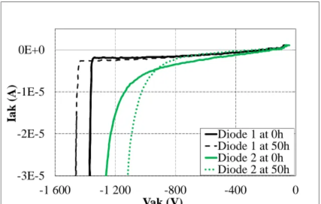
Figure 3 describes electrical reverse characteristics of two DT2 diodes before and after 50 hours passive of thermal ageing (-40°C, +125°C).
Figure 3: Measured I-V reverse characteristics after 50 hours of thermal ageing.
-3E-5 -2E-5 -1E-5 0E+0 -1 600 -1 200 -800 -400 0 Ia k ( A ) Vak (V) Diode 1 at 0h Diode 1 at 50h Diode 2 at 0h Diode 2 at 50h
This figure exhibits the breakdown voltage variations after ageing. An increase or decrease of 100 volts can be observed. In order to explain these variations, samples are prepared for optical observations. Figure 4 presents optical observation of the real component, after 50 hours passive thermal ageing (-40°C, +125°C).
(a) (b)
Figure 4: Optical observation (a) of the entire device and (b) a focus on the trench.
Optical observation does not highlight that peeling of the resin and silicon can explain these variations, and hence, more analyses are requested. Therefore, a simulation approach is proposed.
Thermal variations induce mechanical stress; so it is possible that a separation of materials along the Si/BCB interface and fixed charges appear.
ANSYS is used to localize the maximum stress in the structure after an increase in temperature and TCAD SENTAURUS is used to visualize the electrical characteristics after degradations created in the structure.
4. ANSYS simulations
First of all, using ANSYS Modeler software, a 3D structure of our chip composed of silicon, BCB and gold layers (see table 1 for material properties) was created. Due to the presence of two symmetries, the final structure is 1/4 of the initial structure, as shown in Figure 5. This simplification was used to reduce the simulation time. The major part of the structure was meshed into rectangle elements except for the area near the curved lines where regular trapezia elements were used. The model loading was an isothermal temperature applied to the entire structure in order to obtain the mechanical stress distribution in the structure.
Table 1: Material properties for FEM analysis.
Density (Kg.cm-3) CTE (10-6/°C) Young’s modulus (GPa) Poisson’s ratio Gold 1930 14.2 79 0.44 BCB 1000 42 2.9 0.34 Silicone 2300 2.8 130 0.28
Figure 5: base model of the chip for ANSYS FEM analysis (green = silicon, grey = BCB and blue = gold).
Figure 6 and Figure 7 show the mechanical stress distribution in the BCB and silicon after the thermal load. A logarithmic scale was used to obtain a visual distribution of those mechanical stresses. As expected, the most stressed areas for both materials are located near the BCB/silicon interface on the right angle edge. Indeed, from a geometrical point of view, this geometrical singularity, shown in Figure 7, is the most complex part of the chip structure. Furthermore, the most stressed area of the gold layer is on top of this singularity and the interface BCB/silicon around the trench present high mechanical stress.
Figure 6: Mechanical stress distribution in the BCB (left) and the silicon (right).
Figure 7: Zoom of the BCB and the silicon parts where the most stressed areas are located.
FEM analysis has been useful to understand the behavior of the chip under thermal environment (125°C and isotherm cases) and areas under important mechanical stress have been located on the interface BCB/silicon).
5. TCAD SENTAURUS simulations
The simulated structure is composed by two finite element cells, a base cell and the termination (Figure 8). In order to consider the real die, it is necessary to take into account the different surfaces for each cell. It is necessary to define the Area Factor for the base cell regardless of the termination one.
Figure 8: Base cell and termination.
Sentaurus Device is a single-device simulator, and a mixed-mode device and circuit simulator. A single-device command file is defined through the mesh, contacts, physical models, and solve command specifications [6]. For a multi-device simulation, the command file must include specifications of the mesh (File section), contacts (Electrode section), and physical models (Physics section) for each device. A circuit netlist must be defined to connect the devices (
Figure 9), and solve commands.
Figure 9: multi device simulation and its circuit netlist. Sentaurus Device also provides a number of compact models for use in mixed-mode; in this work Spice has been implemented for defined the system of the circuit (Figure 10): D1, DT present respectively the central and elementary cell.
Figure 10: Circuit for SENTAURUS mixed mode.
5. A. Void created in the structure 5. A.1. Breakdown voltage variations
At the interface Si/BCB, more precisely in internal interface of the termination (Area 1) and external interface of the termination (Area 2), a void with different width (Wv) has been created to observe its impact on the structure.
Figure 11 presents the reverse characteristics after created the void in different parts of the device. A same observation can also be obtained in Area 1 and Area 2 (Figure 8).
(a)
(b)
Figure 11: void width effect on the reverse characteristic in Area 1 (a) and Area 2 (b). These figures exhibit that a separation at the interface does not affect the breakdown voltage. This is explained by the fact that the electric field is concentrated at the end of the field plate and does not make change in this region.
The insertion of a void in the structure at the interface Si/BCB modifies the distribution of potential lines due to the low permittivity of the void (Figure 12). -8E-07 -6E-07 -4E-07 -2E-07 0E+00 -1600 -1200 -800 -400 0 Ia k ( A ) Vak (V) Wv=0.1µm Wv=0.5µm Wv=1µm -8E-07 -6E-07 -4E-07 -2E-07 0 -1600 -1200 -800 -400 0 Ia k ( A ) Vak (V) Wv=0.1µm Wv=0.5µm Wv=1µm
(a)
(b)
Figure 12: The distribution of potential lines in the structure and its zoom with (a) and without (b) void.
This change creates a local increase of the electric field, but remains very low and has no impact in the breakdown voltage of the structure.
Figure 13 presents the impact of the void created in the structure on electrical field along a horizontal cut-line.
(a)
(b)
Figure 13: Electrical filed along a horizontal cut-line (a) and its zoom (b).
It is interesting to observe that electrical field increases in the region near the void; however it has no effect in other regions, that confirms a separation at the interface does not affect the breakdown voltage.
5. A.2. Parasitic capacitance variation
When a reverse voltage is applied to a PN junction, the holes in the P-region are attracted to the anode terminal and electrons in the N-region are attracted to the cathode terminal. The resulting region contains almost no carrier, and is called the depletion region. The depletion region similarly acts to the dielectric of a capacitor, hence the creation of the capacity of the junction.
To check also the proper function of the structure, its capacitance is simulated. Figure 14 presents the capacitance of structure for different value of void.
Figure 14: Effect of the void on the parasitic capacity (Area1).
Figure 14 illustrates that the void created at the interface has no effect on the parasitic capacity. All components have parasitic capacitances as illustrated in Figure 15.
Figure 15: Parasitic capacitances of the structure. Therefore, there are three capacitances: the junction capacitance associated to a depletion region, capacitance associated to the void, and to the BCB. The total capacitance is presented in Figure 16:
0E+00 1E-11 2E-11 3E-11 4E-11 5E-11 0 20 40 60 80 100 C ( F ) Vak (V) Wv=0.1µm Wv=0.5µm Wv=1µm P P Anode Cathode N- N -N+ N+ BCB CBCB CVoid V o id Cj2 Cj1 Gold e1 e2 ej2 ej1
Figure 16: Total parasitic capacitance of the structure. where Cj1 and Cj2 are the junction capacitances, CBCB is
the termination capacitance and the CVoid is the void
capacitance.
The analytical expression of capacitance is given by equation (1)
(1)
Where is the vacuum permittivity
( 8.854 10 , is the relative
permittivity of material, e is the distance between the capacitor's plates, and A is the area of the capacitor's plate (Figure 17).
Figure 17: Capacity model.
The different values of capacitance at -1000V have been calculated in order to decrease the junction capacitances:
BCB Capacitance:
• =3.9
• =3 105µm2 CBCB=98nF
• =105µm
Void capacitance !"# $%&' (
(
• !"#=1
• =4 102µm2 CVoid=33pF
• =105µm
Junction Capacitance D1 ) *& +
+ • ) =11.7 • ) =106µm2 Cj1=1030nF • ) =100µm Junction capacitance DT
) *& +( +( • ) =11.7 • ) =12 104µm2 Cj2=124nF • ) =100µm
It can be noticed that: C
Void<<C
BCB<<C
j2<<C
j1.This result confirms that a vacuum created in the structure has no effect on the electrical characteristic of diode.
5. B. Charge interface insertion 5. B.1. Breakdown voltage variations
Another type of degradation of the simulated structure is the insertion of charge in the interface Si/BCB. Figure 18 illustrates the I-V reverse characteristics with Si/BCB interface charge in Area 1 and Area 2.
(a)
(b)
Figure 18: Traps Effect on the reverse characteristic in Area 1 (a) and Area 2 (b).
The breakdown voltage is modified by the insertion of charge interface in Area 1, but it is not modified in Area 2. Holes insertion creates a virtual P+ vertical doping area and increases the breakdown voltage; while electrons insertion creates a virtual N+ vertical doping area decreases the breakdown voltage. Holes and electrons in Area 2 have not effect in electrical characterization, indeed there is no depletion in this area but charges could have an influence on dynamic behavior. -8E-07 -6E-07 -4E-07 -2E-07 0 -1600 -1200 -800 -400 0 Ia k ( A ) Vak (V) e-traps C=-5E-11cm-2 Widhout traps H-traps C=+5E-11 cm-2 -8E-07 -6E-07 -4E-07 -2E-07 0 -1600 -1200 -800 -400 0 Ia k ( A ) Vak (V) e-traps C=-5E11cm-2 Widhout Traps H-Traps C=+5E-11cm-2
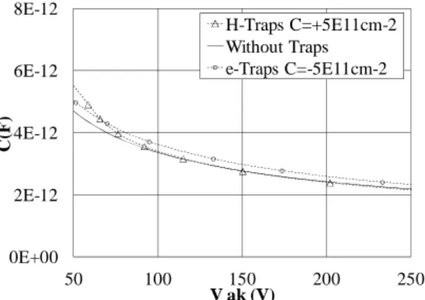
5.B.2. Parasitic capacitance variation
Figure 19 points out the traps effect in the parasitic anode-cathode capacitance for the low value of reverse voltage
.
Figure 19: Effect of the traps on the parasitic capacitance (Area1) for the low value of reverse
voltage.
Indeed holes insertion creates a virtual P+ vertical doping area, so a new P-N horizontal junction as expressed in Figure 20, and in this case the capacitance increases very fast, until the depletion region of the new junction is of maximum width.
P P Anode Cathode N- N -N+ N+ BCB CBCB Cj2 Cj1 Cp Gold (a) (b)
Figure 20: structure capacitance (a) and its equivalent circuit (b).
If it can be imagined that the diode capacitance can be likened to a parallel plate capacitor, then as the plate spacing (i.e. the depletion region width) increases, the capacitance should decrease. Thus, the junction has a variable capacitance that depends on the evolution of the voltage which is applied on it. It is shown that the holes insertion increases the breakdown voltage
therefore increases the depletion region (Figure 22) which causes the decrease of its capacitance (Figure 21); while electrons insertion decreases the breakdown voltage, therefore decreases the depletion region which causes the increase of its capacitance.
Figure 21: Effect of the traps on the parasitic capacity (Area1) for the higher value of BV.
It is observed that for negative charges (e-), the depletion region is smaller than for initial structure. This explains the capacitance rise for a same voltage. Furthermore, it seems the traps can be observed by a capacitance variation.
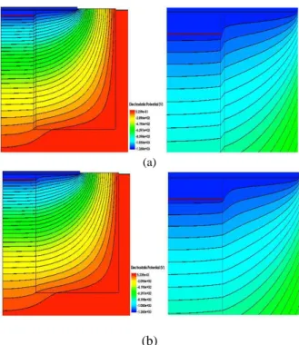
(a) (b)
Figure 22: distribution of potential lines in the structure with e-traps (a) and without traps (b).
6. Conclusion
This paper presents the possibility to use the BCB resin in thick layer to realize deep trench termination.
It can be observed that reverse characteristics changing after 50 hours of power cycling. Optical microscopy could not permit to observed structural modification in order to explain the electrical variations. Thus, TCAD software is used to correlate structural modification with electrical characteristics in order to confirm the presence of the structural modification by combined characteristics.
Delamination on the Si/BCB interface has no impact on the proper function of the interface can not be observed by electrical variation. Moreover, the increasing or the decreasing of the breakdown voltage can be explained by the appearance of a quantity of charge at this interface.
0E+00 1E-11 2E-11 3E-11 4E-11 5E-11 6E-11 0 4 8 12 C (F ) V ak (V) H-Traps C=+5E11cm-2 Without Traps e-Traps C=-5E11cm-2 0E+00 2E-12 4E-12 6E-12 8E-12 50 100 150 200 250 C (F ) V ak (V) H-Traps C=+5E11cm-2 Without Traps e-Traps C=-5E11cm-2
Acknowledgments
This work was supported by the French National Research Agency (ANR) through SUPERSWITCH program (ANR 2011 BS09 033).
References
1. Kamibaba, R., Takahama, K., Omura, I., “Design of trench termination for High Voltage Device”, ISPSD 2010, pp. 107-110, 2010.
2. Théolier, L., Mahfoz-kotb, H., Isoird, K., Morancho, F., “A new junction technique: the Deep Trench Termination (DT2)”, ISPSD 2009, pp. 176-179, 2009.
3. Seto, K., Kamibaba, R., Tsukuda, M., Omura, I., “Universal trench edge termination design”, ISPSD 2012, pp. 161 - 164, 2012.
4. Lee, K.O., Yu, J., Kim, J.Y., Park, I.S., “Thermo-Mechanical Reliability of the Benzocyclebuten (BCB) film in a WLCSP process”, EMAP 2001, pp. 84-87, 2001.
5. Tetelin A., Achen, A., Pouget, V., Pellet, C., Töpper, M., Lachaud, J.L., “Water solubility and diffusivity in BCB resins used in microelectronics packaging and sensor applications”, IMTC 2005, pp. 792-796, 2005.