HAL Id: hal-01710162
https://hal.laas.fr/hal-01710162
Submitted on 19 Feb 2018
HAL is a multi-disciplinary open access
archive for the deposit and dissemination of
sci-entific research documents, whether they are
pub-lished or not. The documents may come from
teaching and research institutions in France or
abroad, or from public or private research centers.
L’archive ouverte pluridisciplinaire HAL, est
destinée au dépôt et à la diffusion de documents
scientifiques de niveau recherche, publiés ou non,
émanant des établissements d’enseignement et de
recherche français ou étrangers, des laboratoires
publics ou privés.
Analyzes of VCO performances based on RF spiral
inductors
Nizar Habbachi, Hatem Boussetta, Mohamed Kallala, Ali Boukabache,
Patrick Pons, Kamel Besbes
To cite this version:
Nizar Habbachi, Hatem Boussetta, Mohamed Kallala, Ali Boukabache, Patrick Pons, et al.. Analyzes
of VCO performances based on RF spiral inductors. International Conference on Engineering and
MIS (ICEMIS 2017), May 2017, Monastir, Tunisia. 7p. �hal-01710162�
Analyzes of VCO performances based on RF spiral inductors
Nizar Habbachi
Microelectronics and Instrumentation Laboratory, Faculty of Sciences of Monastir, University of Monastir, 5000
Monastir, Tunisia, habbachinizar@yahoo.fr
Hatem Boussetta
Institut Prépratoire aux Etudes d’Ingénieurs de Monastir, Rue Ibn Eljazzar - 5019 Monastir Tunisia, and he is with Microelectronics and Instrumentation Laboratory, Faculty
of Sciences of Monastir, University of Monastir, 5000 Monastir, Tunisia,
hatem_boussetta@yahoo.fr Mohamed Adel Kallala
Military Research Centre, Tunis, and he is with Microelectronics and Instrumentation Laboratory, Faculty
of Sciences of Monastir, University of Monastir, 5000 Monastir, Tunisia,
Adel.kallala@gmail.com
Ali Boukabache
Laboratory for Analysis and Architecture of Systems, CNRS , LAAS, 7 avenue du Colonel Roche, 31077 Toulouse, France, and he is with the University of Toulouse,
1077 Toulouse, France, aboukaba@laas.fr
Patrick Pons
Laboratory for Analysis and Architecture of Systems, CNRS, LAAS, 7 avenue du Colonel Roche, 31077
Toulouse, France, ppons@laas.fr Kamel Besbes
Center for Research on Microelectronics & Nanotechnology, CRMN Sousse TechnoPark, BP 334 Sahloul Sousse, Tunisia, and he is with Microelectronics
and Instrumentation Laboratory, Faculty of Sciences of Monastir, University of Monastir, 5000 Monastir, Tunisia,
kamel.besbes@fsm.rnu.tn
ABSTRACT: This paper reports the theoretical study of two different passive RF inductors used to design a voltage-controlled oscillator (VCO) for wireless network at 5GHz. The first inductor is designed using classic microelectronic technology with geometrical optimization and the second is made with etched silicon substrate. The obtained results show a high quality factor Qmax = 12.9 and Qmax=15.9 respectively for the first and second inductors. The self resonant frequencies are higher than 7.5 GHz and allow a large frequency excursion. Moreover, we have used TSMC RF CMOS 0.13 µm technology and the ADS tool in order to design and analyze the responses of two different VCOs based on our RF spiral inductors. The obtained results show a slightly difference between two VCOs. Basically, the second inductor permits to ameliorate the power consumption and the tuning range of the VCO that reach: PC = 0.36 mW and TR = 16.6%. Nevertheless, the phase noise is considerably the same: PN = -102.7dBc/Hz at 1 MHz of offset frequency.
Keywords— CMOS VCO, RF MEMS; spiral inductor; microwave.
I. INTRODUCTION:
The generation of a high spectral signal in radio frequency circuit requires the optimization of Voltage controlled oscillator (VCO). The first VCOs are based on MMIC technology using diode or transistor varactors to vary the oscillation frequency. The example [1] shows the realization of a double tuning VCO based on a heterojunction FET. The results obtained show a variation of 113/92% for the two frequency bands 5,9-12,6/10,6-20,4 GHz. The output power is high PS = 13 to 16 dBm but the major disadvantage is the phase noise PN = -100/-95 dBc/Hz. Another example [2] shows a slight improvement in the variation range of the frequency which reaches Tr = 117% with the use of the heterojunction bipolar transistor (HBT). However, the phase noise remains high PN = -75 dBc/Hz @ 100 kHz with a high power consumption PC = 75 mW. This manufacturing technique is increasingly rejected with the emergence of standard integration processes for RF circuits.
Since the 2000s, the standard technology 0.35 μm is used for RF circuits to reduce power consumption. In the example [3], the VCO is based on the 0.35 μm BiCMOS technology and shows a decrease in PC power consumption = 40 mW and a reduction in phase noise BP = -114 dBc / Hz @ 1 MHz. This improvement is followed by a degradation of the frequency variation range which measures TR = 12.9% and a decrease in the output power PS = -4.5 dBm. Several attempts have been made to improve the performance of VCOs based on the 0.35 μm BiCMOS technology. In a recent work, power consumption is slightly decreased PC = 34 mW with VCO based on the 0.35 μm BiCMOS technology [4].
The miniaturization of the channel length 0.18 μm in RF CMOS technology was accompanied by the presence of new inductance shapes to minimize parasitic effects. Two structures reveal a new architecture based on two quadrature VCOs called QVCO [5-6]. The feat of the new symmetrical differential inductor allowed to maintain a low phase noise PN = -118.67 dBc / Hz @ 1MHz, and the decrease in power consumption PC = 11.8 mW [5]. Similarly for [6], the dual-band QVCO manufactured reveals a better PC =
1.8/4.32 mW and PN = -110/-102 dBc/Hz @ 1 MHz. Nevertheless, the frequency range remains low 11.7% for [5] and 6.1 / 6.7% for [6]. Therefore, it is necessary to use a specific microelectronic technology of fabrication to ameliorate the VCOs performances. In this work, we present two spirals inductor designed and then embedded in VCOs architecture. The first spiral inductor is optimized with geometrical optimization. The second is made with etched substrate in order to decrease the parasitic effects. The aim of our work is to optimize the VCOs performances at 5 GHz. Therefore, the manuscript is divided in two parts. The first investigate the responses of the two different spiral inductors: conventional and MEMS. The second analyses the effect of each inductor on VCO performances.
II. RF SPIRAL INDUCTORS:
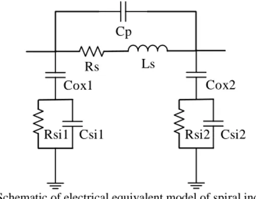
The equivalent model shown in Fig. 1 describes the electrical behavior of on chip RF inductor and is commonly named П model. These elementary components constituting the П model could be useful to estimate the RF inductance performances.
Ls Rs Cp Rsi1 Csi1 Cox1 Rsi2 Csi2 Cox2
Fig.1 Schematic of electrical equivalent model of spiral inductor
In Fig. 1, two parameters are related to the dimension and the conductivity of the spiral coil: Rs represents the series resistance due to the dissipated energy known as ohmic losses, Cp represents the capacitive coupling between two spirals and the amount of stored electrical energy. The isolation between the coil and the underneath passes using an oxide layer causes a parasitic capacitance Cox with the substrate. In addition, the resistivity and the permittivity of the silicon substrate are represented by Rsi and Csi respectively. A. Geometrical optimization
In our case, we have optimized the geometry of the inductor by changing gradually the width of spirals. The Fig. 2 shows a 3D perspective of our spiral inductor:
(a) (b)
Fig. 2 spiral inductor structure (a) 3D perspective (b) top view with detailed dimensions.
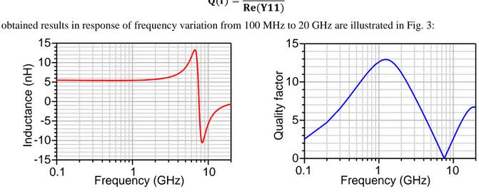
The inductor is constituted by 4.5 turns spaced with 2 µm. The first spiral width is 5 µm and it increases by 5 µm step and reaches 25 µm for the last spiral. We have used a 4 µm layer of copper and a silicon substrate. The inductance and the quality factor values are extracted from the Y parameters using the equations below:
𝐋(𝐟) =𝐈𝐦(𝟏/𝐘𝟏𝟏) 𝟐 ∗ 𝚷 ∗ 𝐟 𝐐(𝐟) =𝐈𝐦(𝐘𝟏𝟏)
𝐑𝐞(𝐘𝟏𝟏)
The obtained results in response of frequency variation from 100 MHz to 20 GHz are illustrated in Fig. 3:
0.1
1
10
-15
-10
-5
0
5
10
15
Ind
ucta
nce
(n
H)
Frequency (GHz)
0.1
1
10
0
5
10
15
Qua
lity fa
ctor
Frequency (GHz)
(a) (b)Fig. 3 Inductor performances in response of frequency variation (a) inductance value (b) quality factor.
The inductor value increases in response of frequency variation and reaches the self-resonant frequency at 7.5 GHz. Indeed, this RF inductor is designed to be used in VCO architecture works at 5GHz where the inductor value is L=8.7 nH. The maximal quality factor is Qmax=12.9 and obtained 1.2 GHz.
B. RF MEMS spiral inductor:
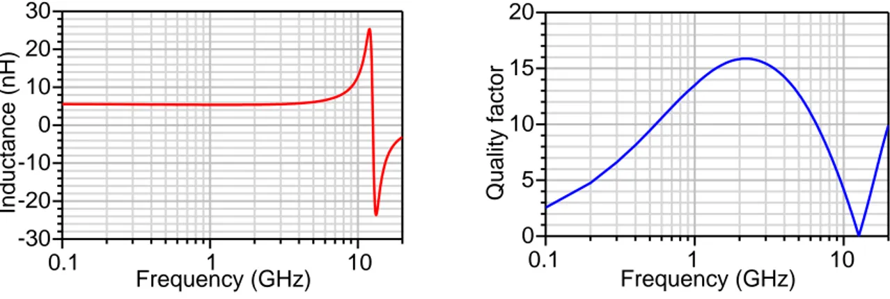
The RF designers need to eliminate all parasitic effects and allow a purely inductance Ls. In order to ameliorate the performances of our inductor we have etched the substrate underneath the spiral core in order to eliminate the substrate and oxide parasites: Rsi, Csi, and Cox. The Fig. 4 presents the new design of RF MEMS spiral inductor:
Fig. 4 3D perspective of RF MEMS spiral inductor
We have analyzed the electrical performances of the new RF MEMS spiral inductor. The Fig. 5 presents the obtained results in response of frequency variation from 100 MHz to 20 GHz:
0.1
1
10
-30
-20
-10
0
10
20
30
Ind
ucta
nce
(n
H)
Frequency (GHz)
0.1
1
10
0
5
10
15
20
Qua
lity fa
ctor
Frequency (GHz)
(a) (b)Fig. 5 Inductor performances in response of frequency variation (a) inductance value (b) quality factor.
As we can see in Fig. 5(b), the inductor value presents a good stability for high frequency levels and L=6.09 nH at 5 GHz. The resonant frequency increases and reaches 12.6 GHz. Moreover, we obtain a important amelioration in quality factor value: Qmax=15.9 at 2.2 GHz.
III. CROSS-COUPLEDCMOSVCO A. VCO using optimized spiral inductor
We have used the TSMC RF CMOS 0.13 µm technology in order to design a conventional cross-coupled CMOS VCO based on RF spiral inductor presented in Fig. 2. The tunable resonator circuit of the VCO is constituted by two NMOS transistors M5/M6 and the spiral inductor. The two NMOS transistors act as actuated varactors controlled by electrical voltage variation. The cross-coupled PMOS M1/M2 and NMOS M3/M4 represent the negative resistance. The oscillation condition is determined by OscTest function included in ADS tool. This function is able to open the looped boucle and measure the S11 parameter. The oscillation occurs when the magnitude of S11 is slightly greater than one and the phase is zero. We have obtained the oscillation condition at 5GHz for a minimal electrical current value of 0.7 mA. Moreover, we have used OscPort function in order to analyze the performance of our VCO. The Fig. 6 presents the architecture and the transistors configurations of our 5GHz VCO:
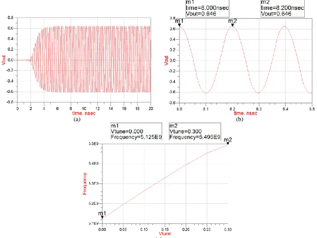
In order to analyze the time domain responses of our VCO we have used a transient simulation. The Fig. 7 presents the output signal shape and the tuning range variation:
(a) (b)
(c)
Fig. 7 Time domain VCO performances (a) start-up time (b) peak voltage value (c) tuning range.
The Fig. 7(a) shows the output signal in response of time for the range of 0 ns and 20 ns. As we can see, the start-up time of the VCO is obtained at 1.5 ns and this result demonstrates the high-speed response of our VCO. In addition, the Fig. 7(b) illustrates the symmetrical sinusoidal oscillation with a period of 0.2 ns and a peak voltage of 0.646V. Moreover, the frequency range is comprised between 5.125 GHz and 5.495 GHz for controlled voltage range 0V to 0.3V. The tuning range value is TR = 7.2%.
One of the most important characteristics in RF domain is the phase noise value. The simulated phase noise and the output spectrum are presented in Fig. 8:
(a) (b)
Fig. 8 Frequency analyzes (a) phase noise response (b) spectral output voltage harmonics.
As we can see in Fig. 8a, the phase noise is about -102.7dBc/Hz at 1 MHz of offset frequency. This result proves that our VCO could be efficient for low phase-noise transmission system. Moreover, the peak output power of our VCO reaches 7.25dBm at a center frequency of 5 GHz and the peak of the second harmonic is less than -24.15dBm (Fig. 8(b)). This result shows high spectral signal ability at 5 GHz.
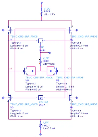
B. VCO based on RF MEMS spiral inductor
A second cross-coupled CMOS VCO is designed using RF MEMS spiral inductor presented in Fig. 4. We have investigated the oscillation condition at 5 GHz and we have obtained an important diminution of electrical current consumption that reaches 0.3 mA. The Fig. 9 presents the new dimensions of used MOS transistors for RF MEMS VCO:
Fig. 9 Cross-coupled CMOS VCO using spiral RF MEMS inductor.
We have analyzed the performances of our VCO for time domain. The Fig. 10 illustrates the different results for a range of 0 ns to 20 ns:
(c)
Fig. 10 Time domain VCO performances (a) start-up time (b) peak voltage value (c) tuning range.
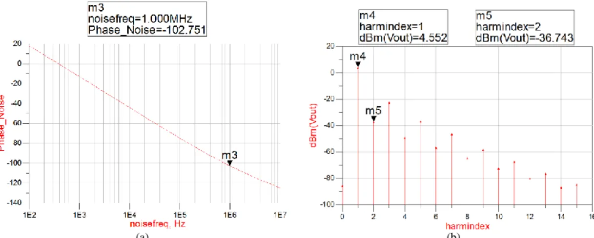
The Fig. 10a shows a start-up time at 2 ns that is close to the previous value obtained in Fig. 7a. The peak voltage reaches 0.48 V and is less to the previous value. Nevertheless, the frequency variation is comprised between 5 GHz and 5.83 GHz that ameliorate the tuning range TR=16.6%. The phase noise and the output spectrum are illustrated in Fig. 8:
(a) (b)
Fig. 11 Frequency analyzes (a) phase noise response (b) spectral output voltage harmonics.
The obtained value of the phase noise is PN = -102.7dBc/Hz at 1 MHz of offset frequency, and it is the same as obtained in Fig. 8a. The delivered output power of our VCO reaches 4.55dBm at a center frequency of 5 GHz and the peak of the second harmonic is less than -36.74dBm (Fig. 11(b)).
IV. CONCLUSION
This paper demonstrates the importance of geometrical optimization and RF MEMS inductors on the amelioration of VCO performances. In two cases we have obtained a low phase noise that reaches PN = -102.7dBc/Hz at 1 MHz, and an important spectral output voltage higher than 4.5dBm. Nevertheless, the RF MEMS inductor increases the tuning range and decreases the power consumption. In the future work, we investigate our tunable microfluidic inductor [7] and capacitor [8-9] on VCO performances.
REFERENCES
[1] E. Reese and J. M. Beall, “Optimized X and Ku band GaAs MMIC varactor tuned FET oscillators” 1988, IEEE MTT-S International Microwave Symposium Digest, pp. 487-490, 1988.
[2] A. Adar and R. Ramachandran, “An HBT MMIC wideband VCO”, 1991 IEEE MTT-S International Microwave Symposium Digest, pp. 247-250, 1991. [3] H. Wu and A. Hajimiri, “A 10GHz CMOS Distributed Voltage Controlled Oscillator Power”, pp. 1-4. 2000
[4] Zhao, Yan, Wang, Zhi-Gong, “20-GHz Differential Colpitts VCO in 0.35-µm BiCMOS”, Journal of Infrared, Millimeter and Terahertz Waves, 2009-03-01, Springer New York, Issn: 1866-6892, pp 250-258, vol 30, issue: 3
[5] S. Ko, J.-geun Kim, T. Song, E. Yoon, and S. Hong, “20 GHz integrated CMOS frequency sources with a quadrature VCO using transformers” 2004 IEE Radio Frequency Integrated Circuits (RFIC) Systems. Digest of Papers, vol. 0, no. C, pp. 269-272, 2004.
[6] N.-jin Oh and S.-gug Lee, “Current reused LC VCOs” IEEE Microwave and Wireless Components Letters, vol. 15, no. 11, pp. 736-738, Nov. 2005.
[7] El Gmati, I., Calmon, P. F., Boukabache, A., Pons, P., Fulcrand, R., Pinon, S., ... & Besbes, K. (2011). Fabrication and evaluation of an on-chip liquid micro-variable inductor. Journal of micromechanics and microengineering, 21(2), 025018.
[8] Habbachi, N., Boussetta, H., Boukabache, A., Kallala, M. A., Pons, P., & Besbes, K. (2016). Tunable MEMS capacitor: influence of fluids. Electronics
Letters.
[9] Habbachi, N., Boussetta, H., Boukabache, A., Kallala, M. A., Pons, P., & Besbes, K. (2016). Fabrication and modeling of a capacitor microfluidically tuned by water. IEEE Electron Device Letters.