Device Design and Process Technology for Sub-100 nm SOI MOSFET's
byAndy Wei
B. S., University of Arizona (1994)
S.M., Massachusetts Institute of Technology (1996)
MASSACHUSETTS INSTITUTE OF TECHNOLOGY
APR 2 4 2001
LIBRARIES
Submitted to the
Department of Electrical Engineering and Computer Science in partial fulfillment of the requirements
for the degree of Doctor of Philosophy
at the
MASSACHUSETTS INSTITUTE OF TECHNOLOGY
ARCHVnES
September, 2000
@ 2000 Massachusetts Institute of Technology All rights reserved.
Signature of Author
Department onmputer Science, September 13, 2000
Certified by
Accepted by
Dimitri A. Antoniadis, Professor, Thesis Supervisor
Arthur C. Smith, Chair, Department Committee on Graduate Students
I
Device Design and Process Technology for Sub-100 nm SOI MOSFET's
byAndy Wei Submitted to the
Deparment of Electrical Engineering and Computer Science on September 13, 2000, in partial fulfillment of the
requirements for the degree of
Doctor of Philosophy in Electrical Engineering and Computer Science
Abstract
Silicon-on-insulator (SOI) MOSFET's are an attractive alternative to bulk-silicon MOSFET's in the sub-100 nm gate length regime due to improved performance and/or scalability. The SOI layer thickness in SOI MOSFET's can be sized so that the channel is either partially- or fully-depletedof majority carriers. Partially-depleted (PD) SOI MOSFET's are easier to manufacture than fully-depleted (FD) SOI MOSFET's because a thicker SOI film can be used. However, PD-SOI MOSFET's are difficult to design due to floating-body effects. FD-PD-SOI MOSFET's are easier to design and are more scalable than PD-SOI MOSFET's. However, in the sub- 100 nm gate length regime, fully-depleted SOI MOSFET's are difficult to manufacture because a bottom gate is required for electrostatic integrity. In this thesis, floating-body effects in PD-SOI MOSFET's and process technology for fabrication of double-gate FD-SOI MOSFET's will be investigated.
Floating-body effects in PD-SOI MOSFET's result from floating-body voltage modulation by AC and DC changes in source, drain, gate, and substrate terminal voltages. This modulation of the floating-body voltage results in modulation of the drain current. AC modulation of the floating-body voltage occurs through capacitive coupling to rapidly switching terminal voltages. DC modulation of the floating-body voltage occurs through diode currents and impact ionization. Because the time constants of these processes are very different, the DC and AC I-V behavior of floating-body PD-SOI MOSFET's are very different from each other, as well as very different from body-contacted SOI MOSFET's or bulk MOSFET's with the body tied to a fixed voltage. Floating-body effects on I- Vbehavior, how they are important in CMOS digital operation, and how they are affected by device design are described and modeled.
Another consequence of floating-body behavior is history dependence in I-V behavior. Rapid switching of terminal voltages induce nearly-negligible changes in body majority carrier content since body majority carriers are trapped by body-source/drain junction diodes. However, the change in body majority carrier content can become significant over many switching cycles, eventually reaching a "switching-steady-state" value if kept switching (different value for different switching patterns), and can return to the initial value if the terminal voltages are returned to the initial settings and enough time is allowed to reach equilibrium. This "hysteretic" variation of the
body majority hole content is problematic because device I-V behavior changes with changing body majority carrier content. Device design to minimize hysteretic behavior will be presented.
Once the hysteretic I-V behavior of floating-body PD-SOI MOSFET's has been understood, floating-body PD-SOI CMOS technology can be optimized to maximize drive current while minimizing hysteresis. This optimized PD-SOI technology can then be compared to bulk CMOS technology. This was done using the 2-D numerical simulator MEDICI in a optimization framework based on the International Technology Roadmap for Semiconductors for the 100 nm-, 70 nm-, and 50 nm-technology nodes.
And finally, double-gate fully-depleted SOI MOSFET's technology was explored. A method to fabricate bury a bottom-gate under a FD-SOI MOSFET was developed based on a flip-bond-transfer technique. This technique is based on chemical-mechanical-polish and wafer fusion bonding. Double-gate SOI MOSFET's were fabricated based with this technique, and a self-alignment scheme for self-alignment of the bottom-gate which to the top-gate was explored.
Thesis Supervisor: Dimitri A. Antoniadis Title: Professor
Acknowledgments
I would like to thank Professor Dimitri Antoniadis for his guidance, technical and otherwise, throughout my graduate school career. The intellectual freedom he affords and encourages has made my time here very productive, both personally and professionally.
I would like thank all the fellow students in Dimitri's research group for all the help, knowledge, and assorted truisms passed back and forth over the years -- in order of appearance: Lisa Su, Jarvis Jacobs, Melanie Sherony, Hang Hu, Keith Jackson, Isabel Yang, Mark Armstrong, Tony Lochtefeld, Hasan Nayfeh, Zachary Lee, Ilia Sokolinski, Andy Ritenour, Ihsan Djomehri, and Isaac Lauer. I'd like to thank Ihsan Djomehri for generating the 2-D doping profiles used in the simulations, Tom Langdo for silicon selective epitaxial growth, and Cristina Gordy and Eda Munro for help with administrative matters.
I would like to thank the entire MTL staff, past and present, for all their help in the fab. In particular, Joe Walsh for all his help with etching and CMP, Bernard Alamariu for help with diffusion, deposition, and other assorted philosophical quandaries, and Paul Tierney for his help with mask-making and photolithography. The staff at MIT Lincoln Laboratories were also great. I'd like to thank Andy Loomis for help developing the wafer bonding process, and Skip Hoyt for wafer grinding. And, above all, it's the friends I've made here that have made the time here that much more enjoyable. Here's to the Miracle of Science (MOS)/Cambridgeport Lecture Series/Friday Night Study Group over the years: Mark, Tony, Ritenour, Fanman, Jim, Isaac, Fletch, Mitch, Kymissis, Arthur Guinness, and Austin Nichols.
Finally, I thank my parents for their support and encouragement through the years. This one's for you.
Project support for this thesis was provided by the Semiconductor Research Corporation, and by the Semiconductor Research Corporation Graduate Fellowship Program.
5
Table of Contents
L ist of F igures ... ... 8
L ist of Tables ... ... 22
1 Introduction ... ... 23
1.1 Silicon-on-Insulator (SOI) MOSFET's ... ... 23
1.2 SOIMOSFETAdvantages ... 27
1.3 Historical Perspective ... 28
1.4 SOI MOSFET Design Issues ... 31
1.4.1 Partially-Depleted SOI MOSFET's: Floating-Body Effects...32
1.4.2 Fully-Depleted SOI MOSFET's: Scalability ... .. 34
1.5 Scaling into the Sub-100 nm Regime ... 38
1.6 T hesis G oals ... ... 39
2 The Floating Body ... 41
2.1 Bulk vs PD-SOI MOSFET Switching Behavior ... 41
2.2 Body-Terminal Connections ... 49
2.2.1 Terminal-Body Capacitances ... ... 50
2.2.2 Body-Source/Drain Diodes ... 51
2.2.3 Impact Ionization Current Source ... .. ... 57
2.2.4 Gate-Body Current Source ... 58
2.3 Floating-Body Effects in CMOS Digital Operation ... 58
2.3.1 CMOS Digital Operation ... 58
2.3.3 Gate Transfer and Output Characteristics ... 64
2.4 Sum m ary ... ... 68
3 Hysteretic Floating-Body Effects ... 70
3.1 Logic State Threshold Voltage Variation ... ... 71
3.2 Silicon Film Thickness ... 73
3.3 NMOS versus PMOS ... 78
3.4 Pulse Stretching ... ... 80
3.5 Frequency Dependence ... 83
3.6 Hysteresis versus Device Design ... 86
3.7 Simulation Methodology to Determine Threshold Voltage Variation ... 94
3.8 Minimizing Threshold Voltage Variation ... 98
3.9 Sum m ary ... 102
4 PD-SOI CMOS Technology Optimization ... 105
4.1 OFF-Currerent versus ON-Current Figure of Merit ... 105
4.2 Design Variables and Optimization Framework ... 107
4.3 Simulation Details ... 110
4.4 E lectrostatics ... ... 114
4.5 SOI Optimization ... 118
4.6 Sub-100 nm Technologies: Bulk versus SOI ... 122
4.7 Sum m ary ... ... 129
5 Double-Gate MOSFET Technology ... 130
5.1 Process Flow ... ... 131
5.2 Flip-Bond-Transfer Process ... 136
7 5.2.2 CMP Mask Design ... 140 5.2.3 CM P Process ... 142 5.2.4 W afer B onding ... 149 5.2.5 Substrate Removal ... 154 5.3 Device Fabrication ... 156 5.4 Top-Bottom-Gate Self-Alignment ... ... 158
5.4.1 Counterdoping Experim ent ... 161
5.4.2 D iscussion ... 166
5.5 Sum m ary ... 168
6 C onclusions ... ... 169
6.1 Sum m ary ... ... 170
6.2 Self-Aligned Double-Gate MOSFET's ... 171
6.3 3-D SO I Integration ... ... 175
A ppendixA ... ... 177
A ppendix B ... ... 193
List of Figures
1-1 Schematic cross section of MOSFET's fabricated on (a) bulk-silicon and (b)
silicon-on-insulator, SOI. ... ... 24 1-2 Bond and Etchback SOI (BESOI) process for fabricating SOI wafers. Two
bulk-silicon wafers, one of which has a thermally-grown oxide, are fusion bonded. The SOI layer is formed by a combination of mechanical grinding,
chemical etchback, and mechanical polish...25 1-3 Smart-Cut process for fabricating UNIBOND SOI wafers. One bulk-silicon
wafer is implanted with hydrogen ions. The SOI layer is formed by fusion bonding the wafer to another wafer with a thermally-grown oxide, at which time the implanted wafer fractures at the hydrogen implant peak. After touch polish of the rough fractured surface, this process produces a SOI wafer and
a bulk wafer. The bulk wafer can be recycled to fabricate more SOI wafers...26 1-4 Separation by Implantation of Oxygen (SIMOX) process for fabricating SOI
wafers. One bulk-silicon wafers is implanted with oxygen ions. The SOI
layer is formed by thermal treatment ... 27 1-5 (a) Cross section and corresponding layout of a CMOS inverter built on
bulk-silicon in a twin-well process. (b) Cross section and corresponding
layout of a CMOS inverter built on SOI. Dimensions are drawn to scale ... 29 1-6 Schematic representation of depletion regions in a NMOSFET. Shown is
(a) a bulk MOSFET, (b) a partially-depleted SOI MOSFET, and (c) a
fully-depleted SO I M O SFET ... ... 30 1-7 Examples of NMOS DC drain current versus gate voltage characteristics for
(a) bulk MOSFET's, (b) partially-depleted SOI MOSFET's, and (c) fully-depleted SOI MOSFET's. The I-V's shown represent values of IDs for VDs=0.05 V to 2.05 V by 0.5 V steps. The subthreshold swing, S, is indicated
on each plot. ... 31 1-8 Comparison of floating-body and body-contacted SOI MOSFET layouts.
(a) Floating-body. (b) Body-contacted. Due to high body resistance, the body contact may become too resistive with increasing device width. Two body contacts are required for wider devices as shown in (c). (c) Asymmetric body tie with body tied to source. The source and drain are not interchangeable. For very wide devices, this structure can be extended with
m ultiple body-ties. ... ... 33 1-9 Simplified schematic demonstrating fully-depleted SOI film thickness scaling.
9 Shown in the light dashed line is charge controlled by the gate, and in the
bold dashed line charge controlled by the drain. Reduction of SOI film
thickness is necessary to maintain full depletion of the channel...35 1-10 Schematic representation of 2-D channel charge sharing through the buried
oxide in fully-depleted SOI NMOSFET. ... ... 36 1-11 Schematic representation of (a) a scaled fully-depleted SOI NMOSFET with
thin buried oxide, highly doped substrate region, and salicided raised source/ drain. Parasitic capacitances can be further reduced with the structure shown
in (b)... ... 37 1-12 Schematic representation of (a) a double-gate fully-depleted SOI NMOSFET
with asymmetric gates and (b) with symmetric gates. The gate workfunctions
of the symmetric double-gate device are shown as design variables...38 2-1 Definition of (a) OFF-state and (c) ON-state of a NMOSFET in a CMOS
inverter in relation to the logic state OUT-HI and OUT-LO of the CMOS inverter. (b) shows the NMOSFET turning ON with the gate voltage rising
and, after a delay due to load capacitance, the drain voltage falling. ... 42 2-2 Schematic cross section of a bulk NMOSFET in the OFF-state. Arrows
show impact ionization current and drain-body depletion region generation
current flowing to the body contact. ... 43 2-3 Schematic cross section of a bulk NMOSFET switching from the OFF-state
to the ON-state. Arrows show gate-depleted body charge, impact ionization current, and drain-body depletion region generation current flowing to the
body contact ... 44 2-4 Schematic cross section of a SOI NMOSFET in the OFF-state. Arrows show
impact ionization current and drain-body depletion region generation current
flowing into the floating body to forward bias the body-source diode ... 45 2-5 Schematic cross section of a SOI NMOSFET switching from the OFF-state
to the ON-state. Arrows show gate-depleted body charge, impact ionization current, and drain-body depletion region generation current flowing into the
floating body to forward bias the body-source diode. ... 46 2-6 (a) Example of instantaneous transient (dashed lines) and DC (solid lines)
gate subthreshold I-V characteristics for a partially-depleted SOI MOSFET. (b) Schematic showing a the transient drain current changing from the instantaneous value to the DC value for the bias point Vos= 1.5 V and VGs=0.5
2-7 (a) Equivalent representation of the SOI MOSFET floating body. (b) AC network to determine the instantaneous floating-body voltage. (c) DC
network to determine the steady-state floating-body voltage...48 2-8 Schematic of diode I-V characteristics representing an ideal diode (n= 1), a
nonideal diode with generation-recombination current (n=2), and a nonideal diode with tunneling current (n=3). Each vertical division represents a factor
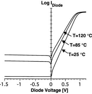
of ten ....5 1 2-9 Diode I-V characteristics of the n=1 diode in figure 2-8, show at T=25, 85,
and 120 'C. Each vertical division represents a factor of ten ... 52 2-10 Diode I-V characteristics of the n=2 diode in figure 2-8. Shown in (a) at
fixed temperature with z=10-10, 10-9, 10-8, 10-7, and 10-6 seconds, and in (b) with fixed carrier lifetime at T=25, 85, and 120 'C. Each vertical division
represents a factor of ten. ...53 2-11 Diode I-V characteristics of the n=3 diode in figure 2-8. Shown in (a) at
fixed temperature with t=10-01 , 10-9, 10-8, 10-7, and 10-6 seconds, and in (b) with fixed carrier lifetime at T=25, 85, and 120 'C. Each vertical division
represents a factor of ten. ... ... 53 2-12 Measured body-source/drain diode I-V characteristics. Diode current is
measured in body-contacted SOI MOSFET's with VG=-1 V. Three devices with three different body doping levels are shown. Higher doping levels exhibit more nonideal behavior resulting in higher ideality factor n. The NA=1x10¹⁸ and 6x10¹⁷ cmr3 have tsi=66 nm, and the NA=5x10 6 cmr3 devices
has t .= 115 nm ... ... 54 2-13 Measured gate transfer I-V characteristics and substrate current due to impact
ionization generation. IDS-VGs and Is,- VG curves correspond from top to bottom to VD=2.01, 1.81, 1.61, 1.41, 1.21, 1.01, 0.81, and 0.01 V. The measured device is a bulk MOSFET with L=O0.1 lm. The saturation
threshold voltage defined at a constant current of 107/Lef A/lpm is shown. ...56 2-14 (a) Schematic showing the NMOSFET in a CMOS inverter. (b) Schematic
showing the switching waveforms on the NMOSFET during a CMOS inverter switch from OUT-HI to OUT-LO which turns the NMOSFET from OFF to
O N ...59
2-15 (a) Schematic NMOSFET gate transfer I-V characteristic and the corresponding ID-VG locus corresponding to figure 2-14. (b) Schematic NMOSFET output I-V characteristic and the corresponding ID-VD locus
2-16 (a) Schematic showing the switching waveforms on a SOI NMOSFET during a CMOS inverter switch from OUT-HI to OUT-LO and corresponding floating-body voltage. (b) Sample gate transfer characteristic showing the difference between floating-body and body-contacted operation. (c) Sample drain output characteristic showing the difference between floating-body and
body-contacted operation ... ... 61 2-17 Graphical representation of the OFF-state floating body voltage without
significant impact ionization (a), and with significant impact ionization (b).
Note the increase in VBO, with significant impact ionization... .... 63 2-18 Schematic showing the dependence of VB,OF on the symmetry between
forward and reverse bias diode characteristics. n refers to forward bias diode
ideality factor... ... 64 2-19 Relevant capacitive divider for determination of subthreshold slope for a
bulk or body-contacted SOI MOSFET (a), and for a floating-body SOI
M O SFE T (b). ... ... 65 2-20 Schematic showing gate transfer I-V characteristic changing versus VB OFF
independent of changes in body-source/drain capacitance ... 67 2-21 Schematic showing what happens to I-V's when body-source/drain
capacitance changes independent of VBOFF. Decreasing body-source/drain capacitance increases the gate-body current boost and decreases drain-body current drag. (a) shows the affect on the body voltage through a switch as defined in figure 2-16, (b) shows the effect on gate transfer I-V's, and (c)
shows the effect on the output characteristics...67 3-1 (a) Two stages in a CMOS invert chain, with NMOSFET's highlighted, in
steady-state then switching from input-LO to input-HI. The first stage begins HI and switches to LO. The second stage begins in output-LO and switches to output-HI. (b) Schematic showing the preswitch voltage,
VB,prel, and hole content in the first-stage NMOS in the OFF-state (OUT-HI),
before switching-ON. (c) Schematic showing the second-stage NMOS hole content and body voltage in the ON-state (OUT-LO). When the first stage switches, the second-stage NMOS switches to the OFF-state (OUT-HI). Due to near-instantaneous switching, the second-stage NMOS maintains the body hole content it had in the ON-state (OUT-LO). The second-stage preswitch
voltage, VB,pre2, reflects the body hole content from the OUT-LO condition...72
3-2 Schematic showing major NMOS body depletion regions in OUT-LO and OUT-HI logic states. (a) Body-contacted devices are shown for reference. The floating-body case is shown in (b). In OUT-HI, there are more holes than when body-contacted due to VB=VB,p,>O shrinking the depletion regions.
OUT-LO is the same as the body-contacted case since the body voltage floats
to 0 V ... 74 3-3 (a) Body hole content and (b) preswitch body voltage versus silicon film
thickness for a NMOSFET starting OUT-HI and starting OUT-LO. Note that the silicon film thickness where OUT-HI and OUT-LO are equal denotes
"charge-balance" ... 75 3-4 (a) Subthreshold gate transfer characteristics for a NMOSFET starting
OUT-HI and starting OUT-LO. In this example tsi=140 nm. (b) Threshold voltage versus silicon film thickness for a NMOSFET starting OUT-HI and starting OUT-LO. Note that the silicon film thickness where OUT-HI and OUT-LO
are equal denotes "charge-balance". ... 76 3-5 Schematic showing NMOS body hole content trend versus silicon film
thickness. For a given gate length and power supply voltage, the silicon film thickness determines whether (a) OUT-HI has more holes than OUT-LO, (b) OUT-HI and OUT-LO are charge-balanced, or (c) OUT-HI has fewer holes
than O U T-L O . ... 77 3-6 Schematic showing NMOS and PMOS equilibrium body majority carrier
content in a CMOS inverter with (a) OUT-HI and (b) OUT-LO. NMOS and
PM OS are com plem entary. ... 78 3-7 Relative device switching speed starting from equilibrium with silicon film
thickness (a) less than charge-balanced, (b) charge-balanced, and (c) thicker than balanced for NMOS and PMOS. Note that NMOS charge-balanced silicon film thickness may be different than PMOS charge-charge-balanced
silicon film thickness...79 3-8 CMOS inverter chain showing which devices propagate the (a) rising edge
of the input pulse and (b) the falling edge of the input pulse... ... 80 3-9 Output pulse stretching versus silicon film thickness relative to
charge-balance. This figure assumes that all devices are in equilibrium prior to the input pulse. (a) The output pulse stretches if both NMOS and PMOS silicon film thicknesses are less than the charge-balanced thickness. (b) The output pulsewidth is equal to the input pulsewidth if NMOS and PMOS are both charge-balanced. (c) The output pulse compresses if both NMOS and PMOS silicon film thicknesses are greater than charge-balanced. Given enough stages, the pulse will cease to propagate and disappear. Note that NMOS balanced silicon film thickness may be different than PMOS
charge-balanced silicon film thickness. ... 81 3-10 Pulse stretching measured in a 480-stage CMOS inverter chain at various
supply voltages. The input pulse is 10 ns wide. The output pulse is shown in bold. The input pulse frequency is 10 Hz. This low frequency is equivalent to starting from equilibrium since there sufficient time between pulses to
restore equilibrium .... ... 82 3-11 Measured pulse stretching per stage for a 480-stage PD-SOI CMOS inverter
chain versus supply voltage at input pulse frequency of 10 Hz. Also plotted is the initial difference in threshold voltage between slower and faster devices, as extracted from SPICE simulation assuming nominal IV7J=0.3 V. Note that
devices are more charge-balanced at higher supply voltage ... 83 3-12 Pulse stretching measured in a 480-stage CMOS inverter chain for VDD=0.8
V at various input pulse frequencies. The input pulse is 10 ns wide. The output pulse is shown in bold. The output pulse stretch decreases at higher frequencies. Measurements only up to 2 MHz were made and state has not been reached. A possible worst-case
switching-steady-state is show n as reference ...84 3-13 Pulse stretching per stage measured in a 480-stage CMOS inverter chain
versus input pulse frequency at various supply voltages. The input pulse is 10 ns wide. Note that switching-steady-state (zero pulse stretch when output pulse width equals input pulse width of 10 ns) occurs at lower frequencies as
supply voltage increases...86 3-14 Output pulse rising edge, midpoint, and falling edge, measured in a
480-stage CMOS inverter chain versus input frequency at various supply voltages. The input pulse is 10 ns wide. Note that the rising edge slows down more
than the trailing edge speeds up ... 87 3-15 MEDICI-simulated example of PD-SOI NMOSFET (LF=O. 12 Rm, NA=6x10'7
cm3, ND= lxl10 9 cm-3, tox=4.5 nm, t,=70 nm, tbox=200 nm) switching in CMOS inverter. (a) Switching starting from OUT-HI logic state. Shown are gate and drain terminal voltage waveforms, body voltage, impact ionization generation rate, hole recombination rate, and body hole content versus time. (b) Switching starting from OUT-LO. (c) Change in body hole content per switch period versus initial body hole content for the device used in this example. Note that the device is not charge-balanced so HI and OUT-LO initial conditions begin with different initial body hole content. Switching-steady-state is reached when the change in body hole content per switch
period equals zero...89 3-16 MEDICI-simulated example of PD-SOI NMOSFET (Le =0.12 jtm, NA=6x10¹⁷
cm-3, N=1lx1019 cm3, tox=4.5 nm, ti=210 nm, tbox=200 nm) switching in CMOS inverter. (a) Switching starting from OUT-HI logic state. Shown are gate and drain terminal voltage waveforms, body voltage, impact ionization
generation rate, hole recombination rate, and body hole content versus time. (b) Switching starting from OUT-LO. (c) Change in body hole content per switch period versus initial body hole content for the device used in this example. Only the silicon film thickness is different between this example and the example in figure 3-14. Note the different switching-steady-state
behavior... ... 91 3-17 Schematic showing NMOS body voltage behavior during the first switching
period starting from OUT-HI and OUT-LO for (a) silicon film thickness less than charge-balanced thickness, (b) charge-balanced, and (c) silicon film thickness greater than charge-balanced thickness. Please refer to figure 3-16 (a) and (b) for definition of the switching period starting from OUT-HI and OUT-LO, respectively. Note the charge-balanced body voltage waveforms are the same whether OUT-HI or OUT-LO, just offset by one
half period. ... 93 3-18 MEDICI simulation example of finding switching-steady-state body hole
content for a NMOSFET. Each symbol represents the same simulation structure at a different initial body hole content, run through a switching cycle. Each curve represents simulations where the switch cycle starts at OUT-HI or OUT-LO. The body hole content which yields zero change in body hole content after a switching cycle is the switching-steady-state body
hole content ... 95 3-19 MEDICI simulation methodology for finding switching-steady-state. The
MOSFET is simulated with external SPICE elements used to mimic NMOS switching in a CMOS inverter. The waveforms are shown to the right of the circuit. Initial body hole content is set prior to the switching cycle by (a) photogeneration into a floating body or (b) an ideal current source into a
contacted body...96 3-20 (a) Switching period definition starting from OUT-HI and body voltage
response. (b) Body voltage relationship to MOSFET logic state and transitions between logic states OUT-HI and OUT-LO. (c) Schematic showing charge-balanced body voltage response to one switching period in which there is no change, a loss of body hole content, or a gain in body hole content (loss and
gain are not to scale). ... 98 3-21 Schematic cross section of SOI MOSFET's with (a) uniform body doping
and (b) nonuniform body doping retrograde channel doping and source/drain halos. The nonuniformly doped body has a higher peak doping resulting in
higher diode ideality factor...99 3-22 Sample body-source/drain diode I-V characteristics simulated in MEDICI
factor... ... 100 3-23 MEDICI simulated threshold voltage hysteresis for different doping profile
types for (a) 0.18 gm technology and (b) 0.13 gm technology designs. The nonuniformly doped halo+SSR profiles show reduced threshold voltage hysteresis compared to uniformly doped profiles. Lower supply voltage
dramatically reduces threshold voltage hysteresis ... 101 3-24 Schematic showing pulse propagation through a CMOS inverter chain versus
silicon film thickness relative to charge-balance. (a) When the silicon film thickness is less than charge-balanced, the first pulse through the inverter chain stretches. In worst-case switching-steady-state the output pulse recovers the input pulsewidth, but the midpoint of the pulse has slowed down relative to the first pulse. (b) When charge-balanced, the output pulse is always the same width as the input pulse, but slows down once it reaches worst-case switching-steady-state. (c) When the silicon film thickness is greater than charge-balanced, the first pulse through the inverter chain compresses, provided that the inverter chain is not long enough for the pulse to disappear altogether. In worst-case switching-steady-state the output pulse recovers the input pulsewidth, but the midpoint of the pulse has slowed down relative
to the first pulse... . . ... 103 4-1 (a) Definition of OFF-current and ON-current on a gate transfer I-V
characteristic. (b) Log OFF-current versus ON-current example for two hypothetical technologies. From left to right, each symbol on each curve represents a gate length. For example, the first symbol on the left of each
curve represents LGATE=L,, the next on each curve represents LGATE=L 2, etc...106
4-2 (a) Definition of terms in scaled MOSFET's. Diagram shows a bulk MOSFET. (b) Definition of design variables in MOSFET's. Diagram shows a SOI MOSFET. Lx, is the source/drain extension length (or the spacer width), N,, is the punchthrough doping density, and t. is the silicon film
thickness... ... 108 4-3 Comparison of body voltage during switching for (a) bulk NMOSFET's and
(b) SOI NMOSFET's. The SOI NMOSFET has VO=VB in the OFF-state,
and turns ON with extra body voltage boost due to capacitive coupling...109 4-4 Left half of simulation structure used to optimize doping profiles to meet
specifications in table 4-1. Doping profile parameterization variables are
shown. The halo is to be optimized at the junction depth in this example... 111 4-5 Sample net doping profile for a 100 nm technology NMOSFET with LGATE= 6 5
nm. In this example the halo was optimized at the junction depth ... 1....12
4-6 100 nm-technology IOFF versus IoN for various body voltages. The peak halo doping is placed at the junction depth in (a) and at half the junction depth in (b). From left to right, the symbols on each curve correspond to LGATE=100,
78,72,65,58,52, and 45 nm... 115 4-7 100 nm-technology IOF, versus IoN for various body voltages. The peak halo
doping is placed at the junction depth in (a) and at half the junction depth in (b). Doping has been modified at each body voltage so that IOFF matches at the nominal gate length 65 nm. From left to right, symbols on each curve
correspond to LGATE= 100, 78,72,65,58,52, and 45 nm ... 116
4-8 IoN vs VB for LGATE= 65 nm devices in figure 4-4. At each VB, the halo doping
has been increased to match IOF, at VB=O V. IoN is degraded by increased subthreshold slope and decreased mobility due to positive body voltage and
increased channel doping, respectively ... 117 4-9 100 nm-technology IOFF vs LGATE at various body voltages from figure 4-4.
Short channel effects (loss of IOFF control with decreasing gate length) are reduced by a combination of body voltage and increased channel doping to
match IOFF at the nominal gate length...118 4-10 Gate transfer I-V characteristics for a 100 nm-technology NMOSFET with
LGATE= 65 nm. (a) Bulk with VB=O V versus VB=0.3 V at the same doping. (b) Bulk with VB=O V versus VB=0.3 V, where the doping has been increased for
the VB=0.3 V case to match VB=O V IOFF. (c) Bulk with VB=0 V versus SOI which as VBOFF=0.3 V with doping adjusted in the SOI case to match bulk V,=0 V Iof Capacitive coupling makes SOI slightly better than bulk at
VB=0.3 V, as shown in more detail in (d) ... 119 4-11 PD-SOI 100 nm-technology V,-hysteresis and Vboost vs LGATE for various
designs shown in above table. Peak halo doping is at the junction depth, x... ... . 121
4-12 PD-SOI 100 nm-technology V,-hysteresis and VBboost vs LGATE for various
designs shown in above table. Peak halo doping is at half the junction depth,
x 2 ... 12 1 4-13 PD-SOI 100 nm-technology V,-hysteresis and Vboost VS tsi for peak halo
doping at the junction depth (Design B in figure 4-11) and at half the junction
depth (D esign E in figure 4-12) ... 122 4-14 100 nm-technology IOFF versus IoN for (a) bulk with halo at the junction depth
versus bulk with halo at half the junction depth, (b) bulk versus SOI (Design B in figure 4-11, V, OF=0.30 V) with halo at the junction depth, (c) bulk versus SOI (Design E in figure 4-12, VB OFF=0.27 V) with halo at half the junction depth, and (d) SOI with halo at the junction depth versus SOI with
halo at the junction depth. From left to right, symbols on each curve
correspond to LGATE=100, 78,72,65,58,52, and 45 nm... ... 123 4-15 70 nm-technology IOF, versus IoN for (a) bulk with halo at the junction depth
versus bulk with halo at half the junction depth, (b) bulk versus SOI (Lext=35
nm, NP,=3x10 8 cmnr3, tsiCB=3 8 nm, VBOFF=0.2 8 V) with halo at the junction depth, (c) bulk versus SOI (Lext=25 nm, NP,=3x1018 cm-3,
tsiCB=70 nm,
VBoFF=0.2 6 V) with halo at half the junction depth, and (d) SOI with halo at the junction depth versus SOI with halo at the junction depth. From left to right, symbols on each curve correspond to LGATE=70, 54,50,45,41,36, and
27 nm .... .... ...125
4-16 50 nm-technology loFF versus IoN for (a) bulk with halo at the junction depth versus bulk with halo at half the junction depth, (b) bulk versus SOI (Lext=25
nm, NP,=4xl0 8 cm-3, tsi,CB= 30 nm,
VBOFF=0.2 3 V) with halo at the junction depth, (c) bulk versus SOI (Lext=20 nm, NP,=5x1018 cm-3
, tsi,CB=6 5 nm, VB,OFF=0.21 V) with halo at half the junction depth, and (d) SOI with halo at
the junction depth versus SOI with halo at the junction depth. From left to right, symbols on each curve correspond to LGATE=50, 38,35,32,29,26, and
22 nm ... ...127
5-1 Schematic cross section of proposed self-aligned double-gate CMOS. Black represents metal and salicide and the dashed lines denote epitaxially grown
raised source/drain... ... 131 5-2 (a) Cross section and side view of starting SOI wafer. (b) Cross section and
side view. The bottom-gate oxide is grown on the SOI. The bottom-gate is formed by deposition of polysilicon, boron implant, patterning, and etching. (c) Cross section and side view. LTO is deposited over the bottom-gate and is densified. The LTO is then chemically-mechanically-polished flat. (d) Cross section and side view. The SOI wafer is flipped and bonded to a handle wafer. (e) Cross section and side view. The SOI wafers substrate and buried oxide are removed. (f) Cross section and side view. LOCOS isolation definition. A SRO is grown and nitride is deposited, patterned, and etched. A field implant is performed. (g) Cross section and side view. LOCOS oxide is grown and the nitride and SRO are stripped. A dummy gate oxide is grown followed by a threshold voltage adjust implant. The dummy gate oxide is the stripped. (h) Cross section and side view. The gate oxide is grown and polysilicon is deposited. The polysilicon is patterned and etched to form the top-gate. (i) Cross section and side view. The top-gate and source drain are implanted. A contact cut to the bottom-gate is patterned and etched. The bottom-gate contact cut is implanted to assure ohmic behavior. (j) Cross section and side view. The bottom-gate is counterdoped to reduce parasitic source/drain-bottom-gate capacitance. Note that a resist mask protects the bottom-gate contact regions during the counterdoping. (k) Cross
--section and side view. A spacer is formed. A raised source/drain is grown by UHVCVD selective epitaxial growth. (1). Cross section and side view. The raised source/drain is salicided. (m) Cross section and side view. LTO is deposited and contact cuts are patterned and etched. Metal is deposited,
patterned, and etched...132 5-3 Cross section of bottom-gate stack prior to CMP. The CMP process was
optimized to flatten a polysilicon step-height of 200 nm. Deposition of 1.5
m LTO resulted in a step-height of 220 nm ... 137 5-4 (a) Schematic top view of the Strausbaugh 6EC CMP machine. Black dots
indicate axes of rotation. Arrows indicate direction of rotation. Double-headed arrows indicate directions of movement. (b) Side view of the wafer
carrier, wafer, table, and pad. The wafer carrier rotates round the quill ... 138
5-5 Schematic demonstrating CMP pattern dependency when using a "soft" pad. (a) When the features are nonuniformly sized and spaced, down force forces the pad into grooves which. Also, the down force per unit area on the larger features is less than for smaller features resulting in removal of smaller features faster than larger features. (b) These effects are reduced with
uniformly spaced and sized patterns ... ... 141 5-6 Pattern dependency of original bottom-gate mask used for double-gate
process. (a) The mask has a great range of feature sizes and spacings. The large features are mainly to the right. (b)-(e) show nonumiformity versus position for 12 points within a die. Nonuniformity is referenced to the point with the thinnest remaining LTO after LTO polish. As LTO is removed, the
pattern dependence becomes apparent ... 143 5-7 Comparison to results of figure 5-6. Shown is the pattern dependency of a
mask from another process. (a) This mask has a much smaller range of feature sizes and more uniform spacing. (b)-(e) show nonumiformity versus position for 12 points within a die. Nonuniformity is referenced to the point with the thinnest remaining LTO after LTO polish. As LTO is removed, the
pattern dependence is much less than the results in figure 5-6 ... 144 5-8 A section from final bottom-gate mask optimized for CMP showing the
addition of dummy CMP lines in between small features. Large features which are not necessary for the NMOS process were removed and replace
w ith dum m y lines... 145 5-9 Measured CMP planarization characteristics. Shown is the LTO step height
versus the amount of oxide removed, which is measured in regions without a step. Two recipes are compared with the down force/back pressure and quill speed/table speed indicated in the legend. In this CMP system, higher
down force and lower speeds are better for planarization... 146
5-10 Schematic showing the need to overpolish. (a) Shows a wafer polished to where the step height is unmeasurable. However, small voids form in regions where dummy CMP lines were discontinuous. (b) This sample was
over-polished and show s no voids... 147 5-11 AFM measurement of LTO surface roughness after water polish versus (a)
down force, and (b) time. These measurements were performed on 1.5 gtm LTO which had been densified at 1000 "C for 10 minutes and CMP-ed to
rem ove 500 nm LTO ... ... 148 5-12 Bond strength versus anneal temperature for hydrophilic SiO2-SiO2 bonding,
and for hydrophobic Si-Si bonding, reproduced from [47]... 150 5-13 (a) Wafer bonding jig shown with a handle wafer, 3 shims, and flat alignment
guides. The SOI wafer is placed face down onto the shims. The alignment guides align the flat. The roller shown in (b) is used to make contact at the
center of the wafer, at which time the 3 shims are removed ... 52 5-14 Photograph of a successfully delaminated SOI layer. However, the edge of
the a wafer was attacked by TMAH etch. The handle wafer thermal oxide at
the edge is not a sufficient mask against TMAH ... ... 155
5-15 Method to protect the edge of the wafer from TMAH. (a) After bond anneal,
the wafer pair is put in LPCVD nitride. (b) The SOI wafer substrate is ground back. (c) An additional layer of PECVD TEOS is deposited just in case the
nitride is damaged during grindback... 155
5-16 (a) Thickness dimensions of fabricated devices. The following plots are for a device with L =0.24 jgm. (b) Top-gate and bottom-gate I-V characteristics. Each is measured with the other gate at 0 V. Each curve represents VDs=0.05,
0.55, 1.05, 1.55, and 2.05 V. (c) Top-Gate I-V characteristic for VDs=0.05 V
versus bottom-gate voltage from -0.5, 0, 0.5, 1.0, 1.5, and 2.0 V. (d) Top-gate output characteristics with bottom-Top-gate voltage at 0 and 1.5 V. Each
curve represents VGs=0.5, 1.0, 1.5, 2.0, and 2.5 V. ... 157 5-17 Schematics of source/drain to bottom-gate overlap demonstrating the
effectiveness of counterdoping. The dashed lines represent depletion region edges. The farther apart the depletion region edges, the smaller the capacitance. (a) Without counterdoping the parasitic source/drain-bottom-gate capacitance is large. (b) Ideal reduction of capacitance occurs when the overlapping region is counterdoped p-. (c) If the counterdope region becomes n, it is capacitively coupled to the source/drain. Thus, the capacitance is between the p-n region in the bottom-gate. (d) If the counterdope is heavy
n , the capacitance is as bad or worse than no counterdoping ... 159 5-18 SUPREM4 as-implanted profiles in the structure with the bottom-gate doped
2x10¹⁹ cmr3, as shown in (a). (b) shows the counterdoped lateral doping profile referenced to the top-gate edge. Note the lateral straggle of the counterdoping implant. (c) shows the counterdoped profile into the
bottom-gate... ... 160 5-19 (a) Resistor array used to experimentally characterize counterdoping implants.
(b) Dimensions of fabricated resistor arrays. The shortest fabricated LGATE
w as 0.2 m ... 162 5-20 (a) Sample resistor I-V for a bottom-gate which has p-type counterdoped
regions. (b) Curvature in the resistor I-V measurement is indicative of the
n-type counterdoped regions ... 163 5-21 Using the low voltage resistance, the geometry of the counterdoped region
can be modeled as a box with depth xd. Lateral subdiffusion, Isd, does not affect long top-gate resistor devices so it is fixed at 0 nm when fitting xd to
measured data as shown in (a). Once the top-gate lengths get shorter, the curve fit is degraded indicating lateral subdiffusion is becoming important. (b) shows resistance versus top-gate length for shorter top-gate lengths for 3
values of lateral subdiffusion ... ... 164 5-22 Doping concentration versus depth into the bottom-gate. (a) Ideal
counterdoping implant profile is flat. (b) Ion implanted profiles are not flat. (c) Adding an extra layer into the implant can flatten out the ion implant
profile... 166 5-23 Schematic showing counterdoping species profiles. The vertical doping
profile of the counterdoping species is shown on the left and the lateral doping profile is shown on the on the right for (a) just counterdoping through the device layers, (b) counterdoping with a spacer, and (c) counterdoping through
an extra layer. ... 167 5-24 Proposed test structure cross section which can characterize the counterdoping
profile with the resistor structure shown on the right, and characterize the effectiveness of counterdoping in reducing capacitance with the capacitor
show n on the left ... 167 6-1 Self-aligned double-gate process proposed in [60]. (a) A chemically-modified
buried layer is formed from the shadow of a gate. The top of the MOSFET is processed to metal, LTO is deposited and polished, and the wafer is flipped, bonded, and transfered onto a handle wafer. (b) The other gate is formed using the chemically-modified buried layer as a mask. (c) The second side
of the M O SFET is processed ... 172 6-2 Schematic representation of layer transfer principles. This example is as
follows: (a) one half of double-gate SOI devices been fabricated, a tungsten plug has been formed, and additional LTO has been deposited as a bonding layer. (b) the wafer is then flipped and bonded to a handle wafer. (c) the substrate and buried oxide are removed, and the other half of the
double-gate SOI device is fabricated... ... 173 6-3 Schematic representation of double-sided interconnects fabricated with the
flip-bond-delam inate process... 174 6-4 Schematic depiction of one "stratum" within a multi-strata 3-D integration.
Shown is a device layer, i-levels of top interconnect, and j-levels of bottom
interconnect... 174 6-5 Schematic of 3-D "semiconductor in insulator" integration showing strata
of device and interconnect layers... 176 ~
List of Tables
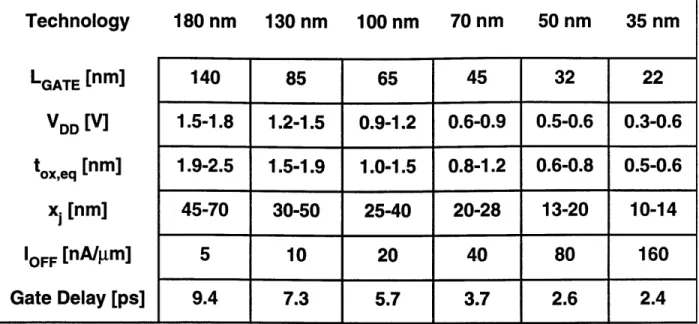
1-1 High-performance logic technology requirements from the International
Technology Roadmap for Semiconductors... 39 4-1 International Technology Roadmap for Semiconductors criteria used to create
doping profiles... . . ... 107 4-2 Optimized doping profile parameters for 100, 70, and 50 nm technologies
with halo set at (a) the junction depth and (b) half the junction depth ... 113
4-3 Peak halo doping concentration used to match IOFF at VB to IoFF at VB=O V for
the 100 nm-technology LGATE= 6 5 nm device with the halo optimized at the
junction depth and at half the junction depth... 114
5-1 CMP recipe used for planarization. Note that the pad conditioner is used in-situ during the main polish. The pad must be flushed out with DI water to remove slurry from the pad. Typically, the main polish is performed on a set of wafers which are kept in a DI water bucket after they are polished. The pad is flushed with running DI water for at least 15 minutes, then each wafer
is w ater polished... ... 148 5-2 AFM measurement of surface roughness. A bare p-prime wafer is used as
reference. tLTO after main polish surface roughness does not include imbedded slurry particles, which were measured to be approximately 200 to
700 nm in size. ... ... 151 5-3 Relative bond strength versus surface treatment and thermal anneal in N
2
am bient... ... 153 5-4 Summary of counterdoping experiment. Listed from left to right are the
type of bottom-gate polysilicon, initial boron dose, arsenic counterdope dose, measured boron concentration, percent activation of boron, whether the resistor I- V's show curvature, the extracted depth of counterdoping, and the
CHAPTER 1. INTRODUCTION
Chapter 1
Introduction
The main advantage of silicon-on-insulator (SOI) CMOS technology versus conventional bulk-silicon CMOS technology is the potential for higher speed operation at the same power or lower power dissipation at the same speed [1]. These advantages are more important as scaling of CMOS technologies becomes more difficult to implement. However, on the transistor- and circuit-level, SOI MOSFET's behave differently than bulk-silicon MOSFET's. These differences in device operation and subsequent differences in device design and scaling are studied in this thesis.
1.1 Silicon-on-Insulator (SOI) MOSFET's
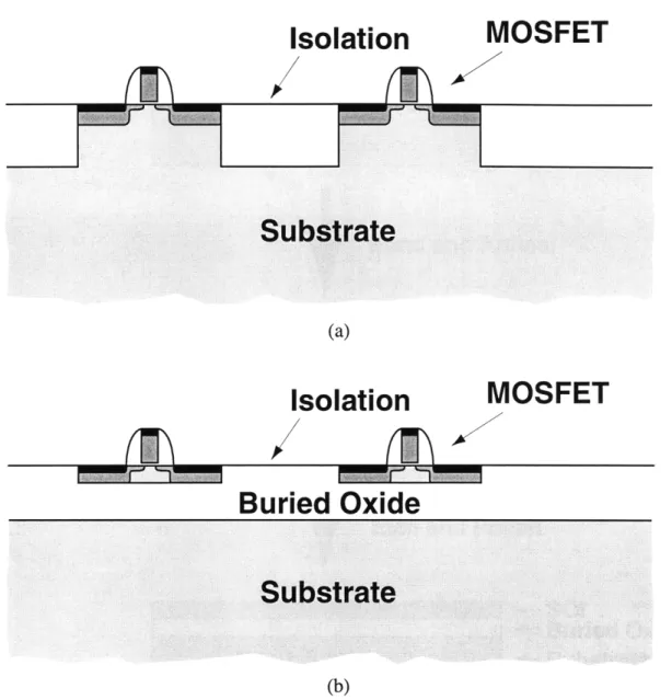
SOI MOSFET's are fabricated on a film of single-crystalline silicon which is separated from the silicon substrate by a layer of silicon dioxide. Figure 1-1 compares a cross sectional representation of bulk MOSFET's to SOI MOSFET's. The buried oxide layer, in conjunction with device isolation, fully isolates the SOI MOSFET with dielectric material.
Three common techniques are used to form the buried oxide layer in SOI wafers. The first is the bond and etchback technique (BESOI) illustrated in Figure 1-2 [2]. A bulk-silicon wafer with
Isolation
CHAPTER 1. INTRODUCTIONMOSFET
(a)Isolation
MOSFET
Buried Oxide
Substrate
(b)Figure 1-1. Schematic cross section of MOSFET's fabricated on (a) bulk-silicon and (b) silicon-on-insulator, SOI.
thermally-grown oxide is fusion bonded to a bare bulk-silicon wafer. One wafer is etched back and polished to the desired silicon film thickness. This process can produce a large range of buried oxide and silicon film thicknesses, but at the cost of two silicon wafers. The second common techniques involves bond and delaminated, in which a piece of one bulk-silicon wafer is transferred to another wafer with an oxide on top. Such processes include Canon's ELTRAN process [3] and SOITEC's Smart-Cut process [4]. The Smart-Cut process is illustrated in Figure 1-3. Again, two bulk-silicon wafer are required, one bare and one with thermally-grown oxide. One wafer has
CHAPTER 1. INTRODUCTION 25
Bulk Si Wafer I
Thermal Oxide
I
Bond and Anneal
Bulk Si Wafer
1
Bulk Si Wafer 2
Etch and Polish
- SOI
Buried Oxide
Bulk Si Wafer 2
Substrate
Figure 1-2. Bond and Etchback SOI (BESOI) process for fabricating SOI wafers. Two bulk-silicon wafers, one of which has a thermally-grown oxide, are fusion bonded. The SOI layer is formed by a combination of mechanical grinding, chemical etchback, and mechanical polish.
hydrogen ions implanted at a depth approximately equal to the desired silicon film thickness. The two wafers are bonded at room temperature. The wafer pair is then annealed at a temperature where the expansion of hydrogen into gas fractures the bonded pair at the hydrogen implant peak. It is then annealed at high temperature to complete the fusion bond. The surfaces at the point of fracture are rough and require polishing. After polishing, the bonded pair of wafers produces one SOI wafer and one bulk wafer. In principle, the bulk wafer can be recycled to process more Smart-Cut wafers. Like BESOI, this process can produce a large range of buried oxide thicknesses but
CHAPTER 1. INTRODUCTION
BulkSi Wafer
I
Implant Hydrogen
Thermal Oyirde Implant Peak
B
B Blk Si
Wafer
1 Bulk Si Wafer 2Bond Bulk Si Wafer 1 Bulk Si Wafer 2 Anneal
Bulk Si Wafer 21
- SOl - Buried Oxide +- Substrate Touch Polish Bulk Si Wafer 2Figure 1-3. Smart-Cut process for fabricating UNIBOND SOI wafers. One bulk-silicon wafer is implanted with hydrogen ions. The SOI layer is formed by fusion bonding the wafer to another wafer with a thermally-grown oxide, at which time the implanted wafer fractures at the hydrogen implant peak. After touch polish of the rough fractured surface, this process produces a SOI wafer
and a bulk wafer. The bulk wafer can be recycled to fabricate more SOI wafers.
IBulk Si Wafer 1
III
CHAPTER 1. INTRODUCTION
Bulk Si Wafer
Implant Oxygen
Amorphised
A-Silicon
~-Implant
Peak
-Si
Wafer
Substrate
*
Anneal
Bulk
Si Wafer
I
SOl
-Buried Oxide
- Substrate
Figure 1-4. Separation by Implantation of Oxygen (SIMOX) process for fabricating SOI wafers. One bulk-silicon wafers is implanted with oxygen ions. The SOI layer is formed by thermal treatment.
silicon film thicknesses are limited by the maximum depth of hydrogen implantation. The third common process, Separation by Implantation of Oxygen (SIMOX), uses only one silicon wafer [5]. As shown in Figure 1-4, the buried oxide layer is formed by a high energy high dose oxygen implant, and high temperature anneal. Due to oxygen implant limitations, silicon film and buried oxide thicknesses are limited [4].
1.2 SOI MOSFET Advantages
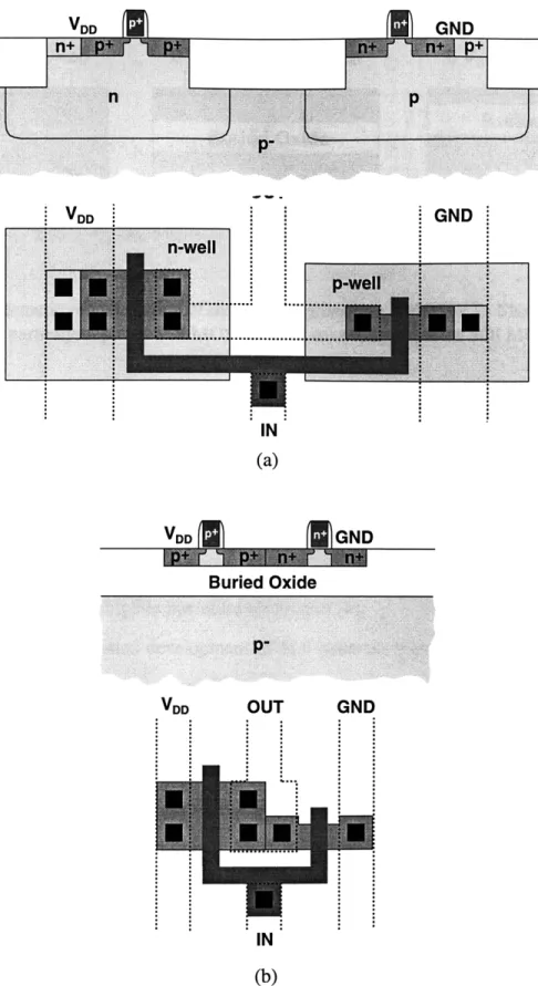
Figure 1-5 compares cross sections and layouts of a CMOS inverter on bulk-silicon to a
CMOS inverter on SOI. In bulk CMOS, the NMOS and PMOS are built in a p-well and n-well, respectively. Parasitic bipolar action between the transistors and the wells can cause a race condition known as latch-up. The transistors and wells must be appropriately spaced and doped to reduce the probability of latch-up. SOI MOSFET's are fabricated on islands of silicon in oxide and thus do not require separate wells for NMOS and PMOS. The NMOS and PMOS can be built in the same silicon island because the drains of the NMOS and PMOS are at the same potential. Thus SOI potentially offers reduced layout complexity, process complexity, and increased packing density
[6].
SOI also offers increased performance on a transistor- and circuit-level. The increased performance is due to much reduced parasitic capacitance between the source/drain and the substrate. Further performance gains can be obtained when the body of the SOI MOSFET is floating. This results in increased drive current due to capacitive coupling to the gate [7]. The floating body also improves pass-gates and logic gates with stacked transistors by reducing the instances of reverse body-source biases [8]. It has been demonstrated that the increased performance of SOI CMOS translates to as much as 30% improvement in CPU speed at the same power consumption of an equivalent bulk CMOS CPU, or a 50% decrease in power consumption at the same speed of an equivalent bulk CMOS CPU [1].
1.3 Historical Perspective
SOI has not been adopted for mainstream CMOS digital logic until just prior to the writing of this thesis [9]. There was a reluctance to adopt SOI technology for mainstream CMOS applications because the performance benefits mentioned above could be obtained by scaling bulk CMOS one generation. Given the historic ease of scaling bulk CMOS, redesign of circuit libraries to take full advantage of SOI as well as the increased substrate cost of SOI could not be justified. As scaling of CMOS has become more difficult due to material and lithography limitations, the potential advantages of SOI are now worthy of consideration for mainstream products.
CHAPTER 1. INTRODUCTION IN (a) VDD (M ( GND Buried Oxide VDD OUT GND IN (b)
Figure 1-5. (a) Cross section and corresponding layout of a CMOS inverter built on bulk-silicon in a twin-well process. (b) Cross section and corresponding layout of a CMOS inverter built on SOI. Dimensions are drawn to scale.
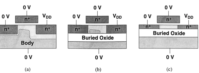
30 CHAPTER 1. INTRODUCTION OV OV OV BBuried Oxide Buried Oxide OV OV OV (a) (b) (c)
Figure 1-6. Schematic representation of depletion regions in a NMOSFET. Shown is (a) a bulk MOSFET, (b) a partially-depleted SOI MOSFET, and (c) a fully-depleted SOI MOSFET.
Prior to current adoption of SOI for mainstream CMOS production, SOI had been manufactured only for niche applications such as radiation-hard electronics and high-temperature electronics. The full dielectric isolation of SOI MOSFET's reduces single-event upsets by shielding the channel region from excess electron-hole pairs generated by alpha particle penetration into the substrate [6]. Similarly, full dielectric isolation limits the source/drain junction area thereby limiting junction leakage currents in high-temperature electronics [6].
Such applications fueled development of SOI material, which in the 1960's and 1970's included techniques such as heteroepitaxial growth of silicon film on a single-crystalline insulator (silicon-on-sapphire, SOS), laser or e-beam recrystallization of polysilicon on oxides (zone-melt-recrystallization, ZMR), or homoepitaxial growth of silicon on oxides (epitaxial lateral overgrowth, ELO). These techniques usually resulted in less than perfect silicon films. SOI MOSFET's thus had inferior performance compared to bulk MOSFET's due to inferior mobilities, high interface trap density at the silicon-insulator interface, high dislocation densities, stacking faults, or grain boundaries. Because of these limitations, SOI MOSFET's were only manufactured for niche applications where bulk MOSFET's could not be used.
In 1977, Izumi, et al., proposed the SIMOX technique of creating the buried oxide layer [5]. Subsequently, the BESOI technique was developed and in recent years the Smart-Cut and ELTRAN
CHAPTER 1. INTRODUCTION
0 0.5 1 1.5 2 -0.5 0 0.5 1
Gate Voltage [V] Gate Voltage [V] Gate Voltage [V]
(a) (b) (c)
Figure 1-7. Examples of NMOS DC drain current versus gate voltage characteristics for (a) bulk MOSFET's, (b) partially-depleted SOI MOSFET's, and (c) fully-depleted SOI MOSFET's. The
I-V's shown represent values of IDS for VDs=0.05 V to 2.05 V by 0.5 V steps. The subthreshold swing, S, is indicated on each plot.
techniques were developed. All these techniques produce SOI wafers with a high quality silicon film which can yield ULSI electronics on par with bulk-silicon wafers [10]. Thus, SOI CMOS for mainstream ULSI applications became a reality, and has become competitive with bulk-silicon CMOS as scaling CMOS technologies becomes more difficult. However, SOI CMOS is not without its problems. Differences in how the SOI MOSFET's operate and scale compared to bulk MOSFET's result in different transistor- and circuit-level design issues.
1.4 SOI MOSFET Design Issues
The buried oxide layer truncates the depth of the MOSFET built on SOI. Thus, SOI MOSFET's can have channels which are either fully depleted or partially depleted of majority carriers, depending on body doping and silicon film thickness. This concept is schematically shown in Figure 1-6 for NMOSFET's. Figure 1-7 shows sample DC subthreshold gate I-V characteristics for a bulk, partially-depleted (PD) SOI, and fully-depleted (FD) SOI NMOSFET.
1.4.1 Partially-Depleted SOI MOSFET's: Floating-Body
Effects
The buried oxide layer leaves the body of the SOI MOSFET floating. While this can be a performance benefit, as noted above, the floating body also introduces anomalous device behavior. For example, the "kink" in the DC subthreshold I-V characteristics of the PD-SOI NMOSFET in Figure 1-7 (b) is due to impact-ionization-generated holes which are trapped in the floating quasi-neutral body region by the potential barrier of the body-source p-n junction [11]. Impact-ionization-generated excess holes raise the body voltage which lowers the threshold voltage.
All other "floating-body effects" arise from the same principle of majority carriers trapped in the body by the potential barrier between the body and source/drain [12-19]. Rather than freely moving in and out of the body through the body contact, the only path for majority carriers in and out of the floating body is through forward bias p-n junction conduction, reverse bias p-n junction space charge region generation, and impact ionization generation. The time constants of these paths are much slower compared to device switching timescales. Thus, when the terminal voltages are changed instantaneously (AC), the body majority carrier content cannot change instantaneously. Over time, currents flowing through the body-source/drain junction diodes and impact ionization generation will change the body majority carrier content as the device settles towards equilibrium
(DC) behavior [20].
This difference between AC and DC behavior results in hysteretic behavior, where the instantaneous MOSFET behavior depends on the switching history of the device. For example, the threshold voltage can start from equilibrium at one value and change over several switching cycles. This makes the floating-body PD-SOI MOSFET difficult to characterize, model, and design. The body of the PD-SOI MOSFET can be contacted, as shown in Figure 1-8. Body-contacted PD-SOI MOSFET's behave exactly like a bulk MOSFET. However, for the same device width, a body contact consumes extra layout area and increases process complexity. So, while body contacts may be selectively used in parts of circuits which cannot tolerate hysteretic behavior, a majority of
CHAPTER 1. INTRODUCTION
(b)
Figure 1-8. Comparison of floating-body and body-contacted SOI MOSFET layouts. (a) Floating-body. (b) Body-contacted. Due to high body resistance, the body contact may become too resistive with increasing device width. Two body contacts are required for wider devices as shown in (c). (c) Asymmetric body tie with body tied to source. The source and drain are not interchangeable. For very wide devices, this structure can be extended with multiple body-ties.
devices should operate with the body floating. Thus, floating-body effects in PD-SOI MOSFET's are an important design issue.
1.4.2 Fully-Depleted SOI MOSFET's: Scalability
FD-SOI MOSFET's display minimized floating-body effects [21,22]. Full-depletion of the body significantly reduces the potential barrier between the body and the source, so majority carriers are not as easily trapped in the body. FD-SOI MOSFET's also have a major advantage because the fully-depleted body allows the surface potential to be directly coupled to the gate voltage [23]. This results in a near-ideal 60 mV/dec subthreshold swing as shown in Figure 1-7 (c). Typical bulk MOSFET's have a subthreshold swing of 80 mV/dec. The subthreshold swing of PD-SOI MOSFET's varies with device design and switching history due to floating-body effects, but is typically between 70 to 85 mV/dec. At the same OFF-state leakage current, improved subthreshold swing allows the FD-SOI MOSFET to operate at a lower threshold voltage, Vr, and achieve increased drain current
due to higher gate overdrive (VDD-VT).
Thus, while a FD-SOI MOSFET is superior to bulk and PD-SOI MOSFET's, it is difficult to scale and manufacture because thin silicon films are required to maintain full depletion of the body. Obviously, a FD-SOI MOSFET without a sufficiently thin silicon film is a PD-SOI MOSFET with all the associated floating-body effects. Maintaining full-depletion of the body is achieved by reducing the silicon film thickness, as shown in Figure 1-9 and can be described as follows: An ideal transistor behaves as a gate-controlled current source. A well-behaved MOSFET should have saturation drain current which is greatly affected by changes in the gate voltage (high transconductance, gm=dIs/dVGs), but minutely affected by changes in the drain voltage (low output conductance, go=dI/dVDS). The level of gate control versus drain control of the drain current is directly related to the relative level of gate control to drain control of body majority carriers and channel charge. For a long channel device with a thin silicon film, the gate controls most of the channel charge compared to the drain. As the channel becomes shorter, the portion of channel
CHAPTER 1. INTRODUCTION CHAPTER ]. INTRODUCTION "...
Buried
Oxide
Reduce
Channel
Length
Buried Oxide
Increase
Channel
Doping
Buried Oxide
Reduce SOI
Thickness
S
D
Buried
Oxide
Figure 1-9. Simplified schematic demonstrating fully-depleted SOI film thickness scaling. Shown in the light dashed line is charge controlled by the gate, and in the bold dashed line charge controlled by the drain. Reduction of SOI film thickness is necessary to maintain full depletion of the channel.
_ _. ._-_ _~~__ 1 - -- I
VDD
B ried A e
Figure 1-10. Schematic representation of 2-D channel charge sharing through the buried oxide in fully-depleted SOI NMOSFET.
charge controlled by the drain versus the gate increases. To counteract this "short-channel effect", the channel doping is increased. This reduces the depletion depth from the gate. As a result, the silicon film thickness must be reduced when the channel length is reduced in order to maintain a fully-depleted channel.
Now, as the gate length is reduced, maintaining a suitable threshold voltage requires higher channel doping densities which in turn requires thinner silicon films in order to achieve full depletion. This is problematic because high channel dopings reduce carrier mobility and thin silicon films are difficult to isolate and contact. In addition, these problems are exacerbated by drain control of channel charge through the buried oxide region, as shown in Figure 1-10 [24]. The field lines from the drain favorably terminate on channel charge rather than on substrate charge due to lower dielectric constant of oxide, and low substrate doping. This "2-D charge-sharing" effect increases drain control of channel charge versus gate control which forces the use of even higher channel doping and even thinner silicon film.
These scaling problems can be alleviated by reducing the buried oxide thickness and inserting a highly doped substrate region beneath the channel region [25]. This highly doped substrate
I
---CHAPTER 1. INTRODUCTION 37
Oxide
(a) (b)
Figure 1-11. Schematic representation of (a) a scaled fully-depleted SOI NMOSFET with thin buried oxide, highly doped substrate region, and salicided raised source/drain. Parasitic capacitances can be further reduced with the structure shown in (b).
region also reduces the channel doping level because of the workfunction difference. A raised source drain can be grown epitaxially to form good electrical contact to the source and drain, and thus low parasitic series resistance [26]. A schematic of an optimized short-channel FD-SOI MOSFET structure is shown in Figure 1-11 (a). This structure can be further optimized to reduce the parasitic source/drain-substrate capacitance by replacing the substrate with oxide and aligning the doped region underneath the channel to the top gate, as shown in Figure 1-11 (b).
If the highly doped region under the channel is contacted, the optimized fully-depleted SOI MOSFET becomes a double-gate MOSFET. A double-gate MOSFET can exhibit increased performance over a single-gate MOSFET if the bottom-gate is used to modulate the MOSFET threshold voltage so that it is low during active periods and high during idle periods [27]. Such a device can be implemented in an asymmetric gate structure shown in Figure 1-12 (a). Further improvement in device performance can be obtained with a symmetric double gate structure by operating both gates simultaneously on an undoped channel region, where the gate material