Assembling 3D MEMS Structures by Folding, Aligning and
Latching 2D Patterned Films
by
Nader S. Shaar
B.S., American University of Beirut
Submitted to the Department of Mechanical Engineering in partial fulfillment of the requirements for the degree of
Doctor of Philosophy
at the
MASSACHUSETTS INSTITUTE OF TECHNOLOGY
MASSACHUSETTS INSiTRE OF TECHNOLOGY
MAY 082014
LIBRARIES
February 2014@
Massachusetts Institute of Technology 2014 /Signature of A uthor... ...
Department of Mechanical Engineering
77 September 26, 2013 Certified bK. /I Certified by. .. . .. . ... ... ... ... ... ... .... ... George Barbastathis Professor of Mechanical Engineering Research Head
...
Carol Livermore Associate Professor, Northeastern University Thesis SupervisorAssembling 3D MEMS Structures by Folding, Aligning and Latching 2D Patterned Films
by Nader S. Shaar
Submitted to the Department of Mechanical Engineering on September 26, 2013, in partial fulfillment of the
requirements for the degree of Doctor of Philosophy
Abstract
The techniques used in the fabrication of micro-electro-mechanical systems (MEMS) were adopted from the integrated circuits (IC) industry and are mostly limited to patterning thin films on a flat substrate. As a consequence, micro-machined devices mostly comprise sets of flat two-dimensional (2D) membranes with etched patterns and undercuts that enable them to serve their intended functions. However, many mechanical, optical and biological applications, such as corner-cube retro reflectors, micro-scale magnetometers, 3D microfluidic systems and 3D photonic crystals, require three-dimensional (3D) geometries for their functionality. In ad-dition, 3D circuits have also emerged as a way of improving connectivity and reducing power dissipation in electronic chips. However, the creation of fully 3D structures via conventional MEMS fabrication techniques typically requires processes that have low throughput, limited control over the final geometry, and higher costs. A promising alternative to 3D microfabrica-tion that addresses these challenges while requiring minimal investment in a new infrastructure is to use the existing technologies to pattern in 2D, and then assemble the patterned segments into 3D structures. Demonstrated methods to achieve that objective have been limited in scope, requiring manual assembly or with limited applicability to specific architectures. This thesis presents a coherent modular system for folding, aligning and latching 2D-patterned precursors into prescribed 3D structures.
The system presented here comprises flexure hinges to enable relative motion among the 2D precursors, a cascaded alignment system to provide progressively better alignment among precursors as they approach their final positions, and systems of reversible latches to retain the assembly in its final configuration while, optionally, permitting disassembly and reassembly of the structure. In particular, two types of systems are considered. First, the design, fabrication and testing of polymer structures with metal hinges, cascaded alignment features and inte-grated latching mechanisms are presented for perpendicular assembly of structures. Second, an alternative latching technique using controlled melting of photoresist polymer adhesive pads is analyzed and tested for the parallel assembly of structures. The structures discussed in this the-sis conthe-sist of SU-8 polymer segments patterned on silicon wafers and linked with an underlying thin gold pattern that defines the hinges. The elasto-plastic bending of the hinges is analyzed and simulated to predict the trajectory and angular position of the membranes during folding. The design of cascaded alignment features, consisting of triangular protrusions and correspond-ing rhombic holes, is discussed. A kinematic model of the alignment mechanism is presented to
demonstrate the effectiveness of the cascading aspect of the design to achieve a large range of angular correction and high alignment accuracy at the same time. The design of micro snap-fit latches that work in conjunction with the alignment system is also presented, and quasi-static simulations of the elastic bending of latches is used to evaluate their strength. Experimental measurements were conducted to characterize the behavior of the gold hinges during bending, demonstrating good agreement with models. The integrated folding-alignment-latching system was demonstrated by assembling corner-cube structures. The alignment process was found to be accurate to within 1 from measurements of the final assembled position of the corner cube structure. The system was also shown to support fabricating reconfigurable devices by demon-strating the ability to unlatch and re-latch segments. The latching and unlatching forces were measured to be 9.7 pN and 12.3 pN respectively.
Research Head: George Barbastathis Title: Professor of Mechanical Engineering
Thesis Supervisor: Carol Livermore
Contents
1 Introduction 16
1.1 Overview of MEMS Development ... ... 17
1.2 3D Microfabrication Techniques . . . . 18
1.2.1 Layering . . . . 19
1.2.2 Direct 3D writing. . . . 20
1.2.3 Building 3D structures from 2D components . . . . 21
1.3 Thesis outline ... ... 23
2 Design 26 2.1 A ctuation . . . . 28
2.2 Hinge Design . . . 30
2.3 Numerical Simulations of Rectangular Hinges . . . . 38
2.4 Constricted Hinges . . . . 45
2.5 Edge-to-Face Alignment and Latching . . . 46
2.5.1 Alignment Features . . . . 47
2.5.2 Micro Snap-Fit Latches . . . . 50
3 Fabrication 53 3.1 Process overview . . . . 53
3.2 Metal layer patterning . . . . 56
3.3 SU-8 patterning. . . . . 58
. . . . 63
4 Experimental Setup and Measurement 4.1 Experimental Setup ...
4.2 4.3
Tools
Magnetic Field Characterization Angular Measurement . . . . 4.3.1 GUI Interface and Usage 4.3.2 GUI Evaluation . . . .
5 Metal Hinge Folding
5.1 Fabricated Devices . . . . 5.2 Folding Measurements . . . . . 5.3 Discussion . . . .
6 Cascaded Mechanical Alignment
6.1 Measurement Protocols . . . .
6.1.1 Coupling measurement . 6.1.2 Final angle measurement
6.2 Experimental Results . . . .
7 Micro Snap-Fit Latches
7.1 Fabrication Results . . . . 7.2 Latching and Unlatching Measurements
8 Face-to-Face Latching
8.1 Concept and Design Considerations . . . 8.1.1 Addition of micro-heaters . . 8.1.2 Structural layer modifications 8.1.3 Patterning the adhesion pads 8.2 Thermal simulations . . . . 8.3 Experimental results . . . . 66 66 68 70 73 75 77 77 78 82 84 . . . . 84 . . . . 86 . . . 88 88 92 92 96 100 101 101 102 102 103 104 3.5 Dry release . . . . . . . .
9 Conclusion 109
9.1 Contributions . . . 109
9.2 Error analysis and reduction. . . . .112
9.3 Roadmap to production . . . .113
9.3.1 Face-to-face interaction . . . .113
9.3.2 Integration of face-to-face and edge-to-face systems . . . 114
9.3.3 Automation . . . 114
A Lithography mask layouts 122 B Fabrication Processes 125 C Software Code 127 C.1 MATLAB GUI code for angular measurements . . . 127
C.2 Arrow-head latch strength simulations . . . 146
List of Figures
2-1 Schematic showing how various interactions of 2D patterned membranes can be
reduced to a combination of edge-to-face and face-to-face interactions. . . . 27
2-2 Lorentz force actuation of a released segment. With the current running into the page, a vertical or horizontal force can be generated by applying a horizontal or vertical magnetic field, respectively . . . 29
2-3 Force and bending moment acting on the gold hinge . . . 30
2-4 Shear force and bending moment distribution along the hinge length . . . 32
2-5 Strain distribution in a beam under bending . . . 32
2-6 Stress vs. strain diagram of gold . . . 33
2-7 Stress distribution in a beam section in the elastic regime . . . 33
2-8 Stress distribution across a hinge section in plastic and elastopoastic deformation 35 2-9 Diagram of a segment during folding . . . 37
2-10 Tip angle deflection of a hinge as a function of the applied vertical force. . . . 39
2-11 Bending moment distribution for vertical loads . . . 40
2-12 Profile of bent hinge for vertical loads. . . . 40
2-13 Force (at 450) vs fold angle of the membrane. . . . 41
2-14 Bending moment distribution for loads at 450 . . . .. 42
2-15 Profile of the bent hinge for loads at 450 . . . 42
2-16 Force vs. deflection angle for horizontal loading . . . 43
2-17 Bending moment distribution for horizontal loads . . . 43
2-18 Bent hinge profile for different horizontal loads . . . 44
2-20 Top views of two fabricated devices showing (a) the straight rectangular gold hinges and (b) the constricted hinges. The dark grey areas are the SU-8 structural segments of the devices and the light grey is the underlying silicon substrate . . . 46 2-21 Schematic diagram of a corner cube structure with three alignment feature pairs
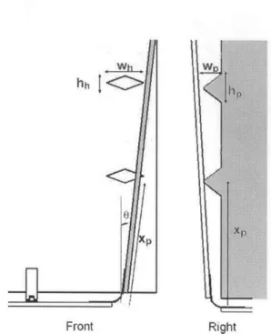
(a) in its flat as-fabricated configuration and (b) during the assembly process . . 47 2-22 Front and side views of the cascaded alignment system at the onset of alignment.
The lower alignment feature pair is engaged while the upper pair is not in contact yet ... ... 48 2-23 Schematic of corner-cube in its final assembled position with a close up view of
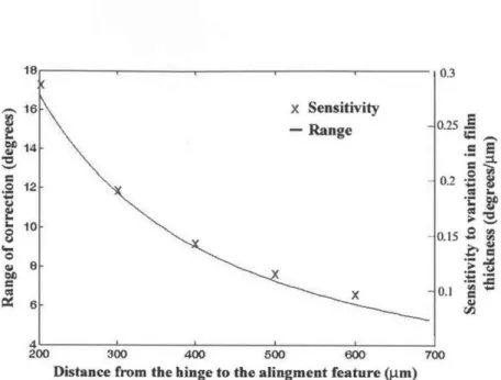
an alignment feature. Section views of the feature pair show the final relative position of the rhombus and the traingle . . . 49 2-24 Plot of the distance from the hinge to the alignment feature vs. range of
correc-tion (left axis) and the sensitivity of the alignment feature to variacorrec-tions in the film thickness (right axis) . . . 50 2-25 Schematic diagram of a latching feature showing the cantilever and arrowhead
tip in their free-standing and loaded configurations . . . 51 2-26 Simulated insertion and extraction forces for a micro snap-fit latch as they vary
with its position relative to the slit in the mating segment . . . . 52
3-1 Schematic of the final fabrication process: gold lift-off, SU-8 spinning and pho-tolithography and XeF2 isotropic dry release etch. . . . . 55 3-2 Optical micrographs of a sample device (a) before and (b) after the XeF2dry
isotropic etch; the last step of the fabrication process. The outline of the resleased segments is highlighted with white lines in (b) for clarity, since the structure is transparent... ... 56 3-3 Schematic of the gold wet etching process. Gold is evaporated on a Silicon
susbtrate, photoresist is patterned on top of the gold layer, the gold layer is etched in sulfuric acid, and, finally, the photoresist is stripped by in an asher with
oxygen
plasma . . . 57 3-4 Optical images of 81Lm gold features patterned (a) by wet etching with a3-5 Optical images of the SU-8 layer during processing. The pattern edges start to appear at the first stage of crosslinking, after the post-exposure bake . . . 59 3-6 Delamination of the SU-8 layer due to prolonged development. The developer
seeps under the polymer layer detaching it from the underlying layers . . . 60 3-7 Schematic of the patterning steps of the photoresist pads, between patterning
the SU-8 layer and the dry release etch in XeF2 plasma . . . 61 3-8 Thickness profile of a photoresist pad after spinning one layer of AZ4620 over
the SU-8 layer (lower curve) and after spinning a second layer (upper curve) . . . 62 3-9 Sample images during the XeF2 release etching step. Devices at 5 different
locations of the wafer were observed after each of 3 rounds of etching. Each round consisted of 90 cycles, each 60 sec long . . . 64
4-1 Images showing the test setup with (a) the device mounted on the ceramic chip holder, (b) the magnetic stack attached to the chip with lead wires connected to the pins of the chip holder, and (c) the circuit board placed under the microscope for m easurement . . . 67 4-2 Lateral measurements of the magnetic field taken on and off the center axis of
the magnet, along the x and y directions. . . . 69 4-3 Normalized magnetic field measurements along the lateral axes (x and y). . . . 70 4-4 Decay of the magnetic field along the vertical, z-axis, away from the magnet.
The zero reference position was chosen to be the surface of the chip holder. . . . 71 4-5 Extrapolated lateral profile of the normalized magnetic field values at different
distances from the surface of the chip holder. The profile becomes flatter as the magnetic flux drops, with increased distance. . . . 72 4-6 Front-end of the MATLAB GUI used for measuring the angular position of the
membranes from optical imagines. The different regions of the interface are highlighted. . . . 74 4-7 Plot of GUI measurements of the test images samples. The actual values of the
angles of the drawn lines are superimposed showing accurate overlap of the data 75 4-8 Means and standard deviations of the errors in the GUI measurement of the
5-1 Optical micrographs of the two types of patterned hinges: (a) straight uniform width and (b) constricted width in the middle section. SU-8 appears as dark grey, hinges appear as a light gold, and the surrounding exposed silicon surface appears as light grey. . . . 78 5-2 Optical image of the patterned gold layer, before adding the SU-8 structural
layer on top, showing the hinges as well as the wires used to actuate the device segm ents. . . . 79 5-3 Sample set of images taken using the microscope camera during the folding of a
segment. The bright line in the image is the edge of the membrane seen from the side. . . . 80 5-4 Current and voltage measurements for a device segment during folding and
re-lease. The data is fitted with a line to predict the resistance in the circuit. . . . . 81 5-5 Tangential component of the Lorentz actuation force vs. deflection angle of the
folded segment for a sample device . . . 81 5-6 Tangential actuation force vs. deflection angle measurements for several devices . 82
6-1 SEM micrograph of a cornercube structure in its initial unfolded configration showing the three aligmnent feature pairs distributed along the edges of the segments to be folded . . . . 85 6-2 Plot of the tangentail actuation force vs. deflection angle of a membrane showing
the elasto-plastic deformation from the initial 380 to the platically deformed state at 700 followed by repeatable elastic cycling of the membrane in a range up to 1050 ... ... ... 87 6-3 Optical snapshots of a device during alignment. The aligning segments is seen
coming fully into focus as it is folded from the back into the imaging plane. The target segment being aligned is seen from the side, as a translucent blur, with its far edge being in focus. . . . 89 6-4 Close-up SEM image of an alignment feature pair with the triangular protrusion
fully inserted into the rhombus hole and aligned to its central axis. . . . 89 6-5 Optical images of a fully assembled cornercube structure from different angles . 90 6-6 Histogram of the angular measurements of the final corner cube assemblies. . . 91
7-1 Mask layout of the first generation latching features showing the dimensions of an arrowhead latch and its corresponding slit . . . 93 7-2 Overlay of the CAD mask pattern onto SEM images of the fabricated latches
and etch holes. The only significant mismatch is the rounding at the corners. . . 94 7-3 Mask layout of the second generation latching features showing (a) the
dimen-sions of the arrowhead profile and (b) an overlay of the cross-section of the corresponding slit in its latched state . . . 95 7-4 SEM images of the two latch designs . . . 95 7-5 SEM image of a fully latched corner-cube structure with 3 alignment pairs and
3 latches... ... 96 7-6 Schematic of the measurement setup with two independant currents used to
actuate the two segments in a vertical external magnetic field. . . . 97 7-7 Raw angle and force measurements of a corner cube segment during latching:
(a) A chronological plot of the angular position (left axis) and the actuation force (right axis). (b) A plot of the force vs. angular position for two cycles of
latching/unlatching
. . . 98 7-8 Actuation force vs. angular position during a latching/unlatching cycle with theforce values offset to account for the spring-back force in the hinge. . . . 99
8-1 Schematic of (a) the overall layout of a device with micro-heaters and (b) a zoom-in onto the corner of the device segment showzoom-ing one of the micro-heaters and the folding actuation wire passing around it . . . 101 8-2 Profile measurements of the photoresist pads after the first spin showing (a) a
relatively uniform thickness in a device with a smaller pad close to the center axis of the wafer, and (b) a sloped profile of the resist in a device with a larger hole that is off-axis . . . 103 8-3 Simulated temperature profiles plotted vs. the radial position along the
photore-sist pad. Temperature profiles are shown for a series of times after the current flow begins (from 0 to 14msec) to capture the profile as it progresses from a starting room temperature profile towards its equilibrium profile. . . . 104 8-4 Step response of the microheater-pad system with an input current of 23mA . . .105
8-5 SEM images of a microscale capacitor prior to folding (top) and with one elec-trode folded and latched on top of the other (bottom) . . . 105 8-6 Optical and SEM images of a photoresist polymer pad in its patterned state (left)
and after melting (right) . . . 107 8-7 A histogram showing the currents required in experiments for melting the AZ
P4620 polymer pads . . . 107
9-1 Representative diagram of a 24-channel LabView-controlled circuit for automat-ing the assembly of the 3D structures. The LabView panel is connected to a data acquisition card that sends serial signals to digital to analog converters, which control the current in a particular channel via a MOSFET transistor circuit. . . . 115
A-i Grid of 14x14 dies patterned on a single 6 inch wafer. Two cross-hair alignment patterns were placed in row #7 of each layer and used to align the mask of a particular layer to a previously patterned film on the wafer. . . . 123 A-2 Mask layout of the structural layer of a corner-cube device showing the two
sidewall segments, marked with 'M' and 'T' patterns. The segments have 3 alignment feature pairs and 3 micro snap-fit latches pattered at the mating edge. The pattern also shows the array of etch holes in the SU-8 layer. . . . 123 A-3 Mask layout of super-capacitor devices showing the six contact pads on the
pe-riphery and the two rectangular electrodes in the middle. The close-up view shows the resistor wire pattern used to heat the photoresist pads. . . . 124
List of Tables
2.1 Material properties for gold . . . . 38
Acknowledgements
This thesis summarizes my research work during my Ph.D. studies at MIT. My experience in the program would not have been as rewarding and enjoyable without the contributions of a great number of people and organizations that have gotten integrated into my daily life at MIT and in the Boston area.
I owe my advisors and thesis committee a great debt of gratitude for their advice, guidance and patience over the last few years. I thank Professor Barbastathis for giving the opportunity to join his research group, and for the numerous mind-stimulating discussions he initiated at group meetings and research discussions. My co-advisor, Professor Livermore, played an instrumental role in jump-starting my research project, keeping it on track, and ensuring that it was completed successfully. I am utterly grateful for her contributions to my education, and I give her a lot of credit for guiding me to the point of finishing my degree. I also thank Professor Slocum for the great perspective that he brought to our meetings and the constructive and supportive feedback he has provided as a member of my thesis committee. I have learned so much about mechanical design from him, and his mode of thinking has been inspirational.
My colleagues in the 3D Optical Systems Group and the Livermore Group have been a great source of knowledge and support. Dr. Tony Nichol and Dr. Hyun Jin In helped me find my way in the microfabrication world and around the fabrication lab. Their feedback was invaluable in growing my knowledge in the domain. My good friend and labmate, Dr. Nick Loomis, was amazingly generous in sharing his knowledge with me, ranging from complex Fourier optics to photography and cycling. I am grateful for all that he has taught me both inside and outside the lab.
Through my involvement with the Graduate Association of Mechanical Engineers, the Lebanese Club at MIT, and the Graduate Student Council I have forged friendships, built relationships, and developed skills that shaped who I am. I feel lucky to have had the opportunity to meet so many brilliant and wonderful people, through those organizations, who made my stay at MIT enjoyable. I am also grateful to my teammates in the MIT Cycling Club and the Boston Team Handball Club for their support and encouragement. Their presence around me was fun and uplifting during my down times.
My family and friends provided support in their unique way. While some did not quite know what I was working on or why it took a long time, their support has been unconditional. I have utmost respect for their understanding, openness and trust. Among them, Zeina, my wife, Wissam, my brother and my dad deserve the most credit for having to deal with my mood swings and grumpiness, particularly during the writing phase of the project. Hiba and Nazih never stopped to believe in my ability to achieve any goals I set for myself, even when they seemed out of reach. Their perseverance was contagious and helped me stay focused when I found myself derailed.
Lastly, there are two people without whom I would not be where I am today - writing the acknowledgements section of a Ph.D. thesis at MIT. Those are my late mom, Hoda Hamdan, and my advisor, Carol Livermore. Unsurprisingly, besides being mothers, they shared quite a few traits from my perspective. They knew me almost better than I knew myself. They were mentors when I needed guidance, and friends when I needed to talk. They shaped who I am and how I think. They had to deal with my flaws and still smiled even when I was giving them a hard time. My mom made sure that I secured my path to start a Ph.D. at MIT, and Carol made sure I left MIT with a Ph.D. I dedicate this thesis to them.
*Thnding for this research work was provided by the Institute for Soldier Nanotechnologies and the National Science Foundation.
Chapter 1
Introduction
In a world where almost every item in our day-to-day life is three-dimensional, it is hard to imagine what it would be like to have tools and objects that can only be a stack of slabs of ma-terial that are cut out using a waterjet cutter and assembled in stacks. The functionality would be constrained that usage of such tools would be limited. That had been the case, to a large extent, with Microelectromechanical Systems (MEMS) for a couple of decades after they came about - tools known to the consumer as: airbag sensors, smartphone tilt sensors, smartphone digital compasses and inkjet cartridge nozzles, to mention a few. For the technically-oriented, MEMS are miniature devices ranging from sub-micrometer and up to a few millimeters, in total size, with functional mechanical elements controlled by electronic circuitry at the micrometer
(micron) and nanometer scales.
The MEMS fabrication technologies were an extension of the integrated circuits (ICs) man-ufacturing technologies. The IC fabrication was two-dimensional (2D) in nature in part because the conventional circuits market required thin flat layouts of conducting wires, sometimes sepa-rated by insulating layers -just like macro-scale printed circuit boards (PCBs). Another reason for the confinement of the fabrication methods to 2D was the adoption of photolithography as the standard method for patterning semiconductor material. Photolithography is a process by which a pattern is transferred from a mask to a photo-sensitive film on a substrate by exposing the film to UV light through the mask then developing it in a chemical. The shallow depth of focus, at high resolutions, implies that a well-defined pattern has to be in the focal plane of the exposure system; hence limiting the patterning to a single plane at a time.
However, the fast growth in the MEMS markets over the last several years and the inherent three-dimensional (3D) nature of MEMS devices has resulted in the development of a greater interest in 3D fabrication [1] [2]. Ironically, even the electronic circuits' development, which had limited MEMS to 2D, has also taken a "3D turn" with the emergence of Thru-Silicon-Via (TSV) technology to enable 3D circuit architectures [3] [4] [5]. Beyond the circuits, the use of the third dimension in building micro-devices provides opportunities for applications that were not possible before, particularly in fields that are inherently 3D, such as biology (BioMEMS) [6] [7], optics [8] [9] [10], microfluidics [11] [12] [13], energy [14] [15] [16] and sensing [17] [18] [19].
Several approaches have been demonstrated in fabricating 3D micro and nano devices. An approach that has the biggest potential of making it into large scale production is one that builds on the existing well-developed 2D fabrication technologies to pattern precursors that are then assembled into 3D structures. The work presented in this thesis is an example of that approach. This chapter sets the stage for presenting the developed technique. The following section puts the MEMS manufacturing into perspective by shedding light on the development of the fabrication technologies over the last half-century. After that a brief survey of other 3D fabrication approaches is presented, paving the way for the discussion of the 3D assembly method proposed in this thesis.
1.1
Overview of MEMS Development
Looking at the historical progression of MEMS fabrication without regard to that of the IC industry, from which it was bred, would be incomplete, if not unjust. The invention of the first transistor at Bell Labs in 1947 triggered the birth of the microelectronics industry [20]. About a decade later, in 1958, the first integrated circuit was created using germanium (Ge) devices at Texas Instruments [21], and soon after that a silicon-based (Si) IC was announced by Fairchild Semiconductor. The latter announcement marked the start of a slow, but full, transition of the IC fabrication technologies to silicon, a transition that spanned about a decade. From that point onward, microfabrication technologies revolving around the patterning of Si-based devices were developed, many of which have remained in use since.
"MEMS" was established. In 1954, the first pressure sensor was manufactured based on piezore-sistive effects in Si. The semiconductor's resistivity proved to be more sensitive to strain than metals, which were used for strain sensing prior to that [22]. By 1958, Si strain gauges were commercially available, leading up to commercial pressure sensor manufacturing that grew into a huge industry - one of the classic examples of a MEMS success story.
The term micromachining emerged to describe the act of carving out silicon patterns using previously developed isotropic and anisotropic etching (1960-1967). Two types of micromachin-ing, bulk micromachining and surface micromachinmicromachin-ing, were distinguished from one another with the former involving etching into the substrate, while the latter was limited to etching of films grown and deposited on the substrate, often making use of 'sacrificial material' layers, the purpose of which is to provide structural support for the device layers during the fabrication process which are removed at the end of the processing.
Despite all the above-mentioned build up in technologies and the utilization of the IC microfabrication tools developed in the 1950's and 1960's to create mechanical sensors as early as the 1950's, it was not until the late 1970's that MEMS, as we know them spread. In 1982, the famous paper by Kurt Petersen, titled "Silicon as a mechanical material," presented a vision of integrating mechanical components patterned into silicon along with the circuits and processors being built on the semiconductor material [23]. The term MEMS - Microelectromechanical Systems -was later established in 1987 in the context of microdynamics workshops. It was used to describe surface micromachined mechanical components that were connected with hinges and moved to perform particular tasks. The term evolved over the last two decades to include multi-billion dollar industries ranging from microfluidic devices to inertial sensors that often are a hybrid of bulk and surface micromachining among many other emerging technologies developed over the last few years.
1.2
3D Microfabrication Techniques
A natural consequence of the development of MEMS from the microelectronics fabrication technologies was that the production tools were good at producing very well defined thin films. The films are typically created with a sequence of two steps starting with an additive process,
where a layer of material is added on top of the substrate, followed by a subtractive process in which parts of the layer are removed and the remaining parts form the patterned layer. In most cases, an optics-based step is performed between the two steps to define the pattern to be 'subtracted'. In some cases, defining the pattern optically in an intermediate film is done prior to the additive step. Based on the pattern, material is selectively added to certain areas of the substrate and not others.
Additive processes include evaporation, sputtering, film growth, electroplating, nano-imprinting and centrifugal spinning of viscous material on a wafer. Subtractive steps include all types of etches, categorized in different ways such as isotropic vs. anisotropic, dry vs. wet and chemical vs. physical. The most common methods used in the optical patterning step are projection lithography, electron beam writing and interference lithography.
Moving to the third dimension has taken several approaches that can be classified into three main categories. One category involves layering 2D patterns in stacks along the third dimension, another is directly writing into a medium to form a 3D object, in a way analogous to lithography in 3D, and a third category consists of assembling thin film segments in 3D orientations to form the desired structure.
1.2.1 Layering
Since the state-of-the-art fabrication techniques are two-dimensional, creating 3D structures simply by stacking 2D patterns on top of one another seems the most natural step towards 3D fabrication. While the techniques following the layering approach implement the classical fabrication methods to define the individual layers, they vary significantly when it comes to how they assemble the layers. The most straight-forward of the techniques is to simply pattern layers on top of one another, with the additive step of a layer following the subtractive step of the previous layer.
Qi et al. demonstrated the fabrication of a 3D photonic crystal using such a technique [24]. Their fabrication method consisted of iteratively patterning 2D silicon films, creating a stacked structure with a 3D pattern of cavities in the silicon. Patel et al. presented an improvement to that fabrication technique demonstrating a significant improvement in yield (66%) and reduction in processing time from months to days [25]. The alternative method
still relied on layering; however, instead of patterning the layers on top of one another, on the same substrate, layers were patterned separately, inspected for defects and stacked if they were defect-free. The technique was recently demonstrated for large-area stacking by Lu et al. [9] Aoki et al. have successfully demonstrated a similar technique using micro positioners to pick up segments of a patterned layer and stack them on top of one another [26]; a method utilized by Tandaechanurat et al. to create high-Q 3D photonic crystals [27].
A third technique, within the layering category, is transfer-patterning of imprinted films, where each layer is patterned on a base substrate and transferred to the destination substrate sequentially creating a stack of the patterned layers, as demonstrated by Han et al. [28].
The biggest advantage of these approaches is the high resolution and reliability of patterning the individual layers, particularly for MEMS scales, because the technology involved in the patterning is tailored to smaller scale industries such.as electronics and photonics. However, the weaknesses lie in the effect of the multiple layers on compromising that quality. In the first technique, one has to choose between removing the sacrificial material at every step, which results in lower layers creating a non-flat topology of the surface for subsequent layer patterning steps, and keeping the sacrificial material, which would require access to all the cavities in the final 3D structure - a limitation on the architecture of the device, as was the choice of Qi et al. For the latter two techniques, the limitations lie in the ability to align the layers with high-enough accuracy and at a high high-enough pace to match the fast throughput of the fabrication of the individual layers.
1.2.2 Direct 3D writing
Another approach to creating 3D patterns is to simply write the patterns in 3D. This is possible by using nonlinear optical sensitivity of photo-patternable material to expose a 3D medium. One technique is to use a 3D optical pattern to expose the resist [29] [30] [31]. Divliansky et al. demonstrated using a single mask with one light source that generates a 3D diffraction profile to expose the resist [29]. Lai et al. followed a different approach by splitting the exposure source beam and using interference lithography with multiple exposures to create the 3D pattern [31].
Another way of writing in 3D is to raster scan the volume, writing one voxel at a time. Focusing a laser beam onto one spot in a block of photoresist and controlling the intensity
allows polymerizing the resist within that voxel only. The photoresist is then scanned in 3D to create the desired polymerized 3D structure. Kawata et al. demonstrated the ability to produce arbitrary shapes in 3D, comparing the results of scanning the full volume to the faster
- but lower quality - approach of patterning the shell then curing the inner parts by flood exposure [32]. Deubel et al. have also demonstrated fabricating a 3D photonic crystal by direct laser write [33]. Similar approaches use the focused laser beam to initiate additive or subtractive processes that are localized to the voxel at the focal point [8] [34].
These techniques compare to the common projection lithography as 3D bench-top printing compares to injection molding, in classic macroscale manufacturing, in terms of cost structure. The former has lower capital costs but is not a good model for mass production, since the cost of manufacturing each product is relatively high. In contrast, projection lithography in-volves setups that are multi-million dollars in cost, so, in the extreme case where one device is manufactured using the set up, the cost of that device would be extremely large; however, the variable cost is low that when millions of devices are produced the cost per device can go down to a few cents.
So, while direct 3D writing is great for making a few custom micro prototypes, it is not suited for mass production. Another limitation of the technique is that patterning enclosed cavities is not possible because the photoresist inside the cavity needs to be developed.
1.2.3 Building 3D structures from 2D components
A third approach to creating 3D microstructures captures the benefits of the layering approach without compromising on the misalignment and potential speed of production throughput. It uses 2D patterning to define high quality thin film with high resolution, using conventional fabrication, and utilizes techniques to create 3D structures from those building blocks. The assembly method presented in this thesis falls into this category. Within this approach the methods used can be classified into two main subcategories. The first is based on the robotic assembly of the 2D components, while the second relies on self-assembly of the patterned segments.
The robotic assembly technique involves the use of microfabricated micro-scale grippers that are mounted on micropositioners and used to pick up fabricated components and assemble
them on a substrate. Contact points are implemented in the components to allow the micro grippers to hold on to them. Breakable tethers are used to hold the components in place until they are picked up. On the assembly side, patterned slits in the substrate are used to place the components while mechanical stoppers in the patterns allow the pieces to support one another [35] [36]. Attempts to automate the robotic assembly in a manner similar to how electronic components are assembled on printed circuit boards have been made [37] [36]; however, while the automation reduces the fabrication cost, it falls short of matching the production rate of the components, given the batch fabrication capabilities of foundries.
The Nanostructured OrigamiT M project is a classic example of the self-assembly technique [38]. Nanopatterned films are shown to fold about creases upon their release [39]. Films of different types have been demonstrated including ceramics (SiN) [39], polymers (SU-8) [40] and silicon [41]. Several methods for folding are also demonstrated. Stressed bilayers of chromium on silicon nitride films are shown to fold the membranes to angles specified by the dimensions of the chromium pattern. Nanomagnets patterned in plane as well as magnetic tips of carbon nanotubes are shown to provide enough magnetic torque in a rotating external magnetic field to rotate the membranes [42]. Stresses in SiN films are also shown to be induced by helium (He) ion implantation and fold the hinges as well [43]. Other 3D self assembly methods have also been demonstrated. Surface tension of melted solder patterns and thermal polymer bimorphs have been demonstrated as effective folding mechanisms. Nanomagnet arrays have also been demonstrated to provide in-plane alignment and latching between membranes with arrays of matching magnetizations [44].
Of all the approaches used to fabricate in 3D, the one that is most promising is the origami-like self-assembly approach. The method capitalizes on the fabrication capabilities of the current state-of-the-art technologies in the field, eliminating the need to investment in new technologies. However, the techniques demonstrated in the literature only focus on one aspect of the assembly process. A black-box solution that takes a 2D pattern and produces a 3D structure has still not been shown. Moreover, while the out-of-plane folding techniques have been extensively studied and impressive results have been shown, the alignment of the folded membranes and methods of reliably fixing them in their final configurations are not as well developed.
1.3
Thesis outline
This thesis presents an integrated system for assembling 3D micro devices from 2D patterned precursors. The design, modeling, fabrication and testing of the folding, alignment and latching components of the system are discussed as follows. In Chapter 2, the theoretical modeling and mechanical design of the hinges, alignment features and micro snap-fit latches is discussed. Section 2.1 describes the Lorentz force actuation method used in the assembly process and defines the loading effects of those forces on the hinges. Subject to those loads, the mechanics of the hinge bending are modeled in Section 2.2, addressing both the elastic and plastic regimes of the hinge deformations to predict their profiles. Numerical simulations, based on the developed models, are then presented in Section 2.3, and a modified design of hinges with constrictions is adopted allowing for better controlled folds with localized bending of the film. The design and modeling of alignment and latching features are also presented. The kinematic constraints defining the behavior of the alignment system is discussed in Section 2.5.1, highlighting the importance of cascading the features in achieving a combination of high accuracy and large correction range. Section 2.5.2 addresses the mechanics of the micro snap-fit latches used to hold the folded segments together and presents a simple elastic model of the small deformations they undergo in the latching/unlatching processes.
Chapter 3 focuses on the clean-room fabrication process used to manufacture the 2D mem-branes before they are folded. A general overview of the fabrication process is first presented
(Section 3.1), then the detailed processing steps and parameters for each layer are discussed. Section 3.2 compares the two investigated methods of patterning the metal layer, wet etching and lift-off, showing the superiority of the latter in producing cleaner patterns with better controlled feature dimensions. An optimized process for patterning the structural layer, SU-8 2015, is outlined in Section 3.3, including recommendations for the exposure, development and baking of the film to minimize residual stress in the film and maximize adhesion to the under-lying metal layer. The protocol for defining adhesion pads, used in some devices, is covered in Section 3.4. That step is particularly interesting, because the photoresist used to make the pads is patterned into existing trenches that are twice as deep as its spun thickness, which requires a double-spin of the resist. Lastly, the isotropic XeF2 dry release etch is analyzed in Section 3.5. Etch rates are compared at different positions on the wafer and across different etch hole sizes.
Chapter 4 describes the experimental setup as well as the measurement tools and procedures used in the testing of the fabricated devices. Section 4.1 compares two test assemblies and evaluates the pros and cons of each, and explaining the choice of using a stack of magnets under the device's chip holder as the magnetic source for the Lorentz actuation. Then, Section 4.2 presents the characterization of the magnetic field distribution in the device cavity, for the chosen setup. Section 4.3 provides an overview of the image processing MATLAB tool used to measure the angular position of the folded membranes. The tool uses the user's input to trace the edge of the membrane and calculate its angle. The tool's measurement accuracy was evaluated using CAD-generated images and found to be within 0.150 (~2 mrad).
Chapters 5, 6 and 7 present the experimental results obtained from testing the different aspects of the systems. For the hinge folding, a characterization of the fabricated patterns of the hinges and actuation wire loops is first introduced, describing the achieved variations in film thicknesses and pattern dimensions (Section 5.1). The details of the measurement procedures and the collected results are then discussed in Sections 5.2 and 5.3. A correlation between the applied force and the fold angle for the hinges is established in order to allow open loop control of the folding to within the alignment correction range. The alignment system testing is then presented in Chapter 6. For the fabricated devices, it is shown that the system's cascaded features allowed for angular corrections from misalignments of up to
+/
- 110 to within 0.5' nominal accuracy. Potential source of error in the final alignment and suggestions to improve on that are presented in Section 7.2. The test results of the latching mechanisms that hold the aligned segments together, in their final configuration, are discussed in Chapter 7. The resistive force of the latches as well as their retention force are characterized and the ability to produce re-configurable devices is demonstrated, by repeatedly latching and unlatching the same devices.Chapter 8 is a stand-alone chapter that addresses the particular case of assembling segments into stack-like structures, in which the faces of the mating come into contact. The presented solution is based on locally heated adhesion pads that melt and fuse together. First order thermal modeling is used to predict the currents required to melt the pads (Section 8.2) and experimental support for the model is presented, based on melting currents for fabricated pads
The thesis concludes with a summary of contributions and proposed advancements to take this fabrication technique to the level of large volume production
Chapter 2
Design
The objective of assembling 3D micro devices from 2D patterns can be divided into three fundamental functional requirements: folding, alignment and latching. This chapter focuses on the design considerations taken in achieving those three functions in fabricated microstructures. However, before diving into the design, we need to define some of the terminology used and lay out some basic assumptions about the devices at hand. The devices are assumed to consist of flat thin membranes of finite uniform thickness, by virtue of the photolithographic thin film patterning used. Upon the completion of the fabrication process, the devices consist of a 2D layout of patterned pieces of film. Those pieces are referred to as segments and are connected to one another with hinges. The device segments are folded about the hinges and consequently assembled into a 3D structure. To make the design process manageable, we make the following two observations:
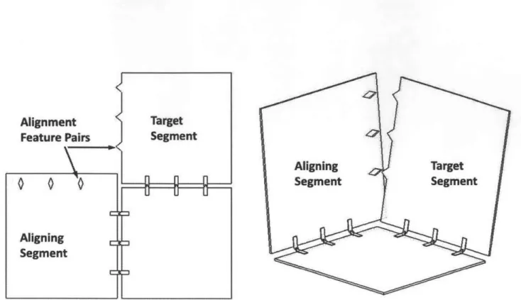
1. The interaction between device segments can be itemized as interactions between pairs of segments at a time. Three segments engaging together can be thought of as two segments each engaging with a common third segment.
2. As two segments engage in some sort of interaction, be it mutual folding, relative alignment or latching to one another, they may do that in two modes. The first is an edge-to-face interaction, with the edge of one segment interacting with the face of the other, as is the case with assembling a T-like geometry. The second is face-to-face interaction, as is the case with building a stack of segments. Figures 2-1a and 2-1b illustrate the two
(a) (b)
(C)
(d)
Figure 2-1: Schematic showing how various interactions of 2D patterned membranes can be reduced to a combination of edge-to-face and face-to-face interactions.
modes. An edge-to-edge interaction can be reduced to an edge-to-face or a face-to-face interaction by adding an extension to one of the membranes or adding an intermediate assembly-supporting membrane (Figure 2-1c-d).
The focus of the work reported in this thesis is on the edge-to-face interaction mode. As-semblies with face-to-face interactions were demonstrated and are reported, as well, but to a smaller extent. In this chapter we start with a quick overview of the actuation method used in the assembly process and a discussion of the design of the hinges about which the segments fold, both of which are at the heart of the concept of making 3D objects from the 2D patterns. Then, we discuss the alignment and latching features designed for the edge-to-face interaction of segments. Chapter 8 reports on the design of the photoresist adhesive pads and the use of micro-heaters to selectively activate the pads for the face-to-face interaction.
2.1
Actuation
The patterned devices were actuated by running a current through a wire in the suspended sections and applying an external magnetic field, resulting in a Lorentz force on each wire segment given by
F =iL x B (2.1)
where L is a vector whose magnitude is equal to the length of the wire segment shown in Figure 2-2, and whose direction is the same as that of the current flowing through it. B is the applied external magnetic field. By virtue of the cross product relationship, applying a horizontal magnetic field while running a current through the wire loop generates a vertical force that folds the segment out of plane (Figure 2-2b). Similarly, a vertical magnetic field results in a horizontal actuation force. (Figure 2-2c).
This actuation method has several advantages over other methods found in the literature, such as stressed by-layers [39], nanomagnets [44] and thermal bimorphs [45]. For a set external magnetic field, this method allows to selectively apply forces to specific segments, in specific directions, by running a current throw those segments' actuation wire-loops. It also allows for a highly accurate control of the force, independently of the device structure, simply by varying the magnitude of the current, which can be used to de-couple the applied force and the position
(a) d v is F BI (side views) F( B (b) (c)
Figure 2-2: Lorentz force actuation of a released segment. With the current running into the page, a vertical or horizontal force can be generated by applying a horizontal or vertical magnetic field, respectively
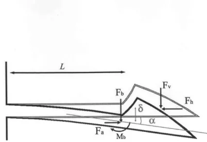
F
E IN
Ls
Mt
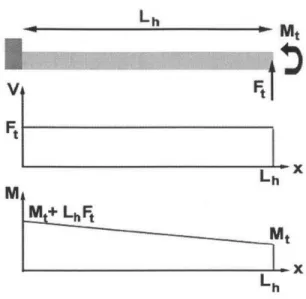
Figure 2-3: Lorentz actuation force translates to a force and a bending moment at the hinge tip
of the folded segment. The price to pay for all those features is mostly in real estate. Supplying independent wire loops for each segment of a complex device may be challenging, particularly when a segment is connected to the substrate through multiple other segments. In the latter case, the wire that actuates the segment needs to be navigated through the segments that connect it to the substrate where the contact pads typically are.
Having adopted this method of actuation, our analysis of the folding mechanism assumes a force acting at the tip of the folded segment, distributed along the edge parallel to the hinge.
2.2
Hinge Design
For the purpose of modeling the system, given the micro-scale of the actuated segments, the variation of the magnetic field along their tip is assumed to be negligible. Hence, the distributed actuation force is considered to be uniform along the wire segment. To avoid any twisting of the segments during the folding process, the hinges are distributed symmetrically along the segments' edges. That results in a symmetrical distribution of the load on the multiple gold hinges connecting the two structural segments. Subsequently, the analysis of the folding mechanism can be reduced to a two-dimensional analysis as depicted in Figure 2-3.
A generic force applied to the actuated segment at an angle OF from the vertical, translates to a transverse force Ft, an axial force F and a moment Mt at the tip of the hinge where, for
a segment of length L, in the starting flat configuration,
Ft = F cos(OF)
Ft'= F sin (OF)
Mt = FL8 cos(OF).
The axial force results in minimal axial elongation and does not affect the profile of the bent hinge; however, the transverse force and moment generate a distribution of internal shear force and internal bending moment along the hinge length, which govern its bending proffle.
The gravitational force is ignored in the analysis, since the weight of a 1mm x 1mm x 10pm
SU-8 membrane is on the order of 0.1pN, while the magnetic forces during the assembly are
on the order of 10pN - about 2 orders of magnitude larger.
At a distance x from the base of the hinge, the internal shear force V and bending moment
M are, hence, given by
V(x) = Ft (2.2)
M(x) = Mt +
J
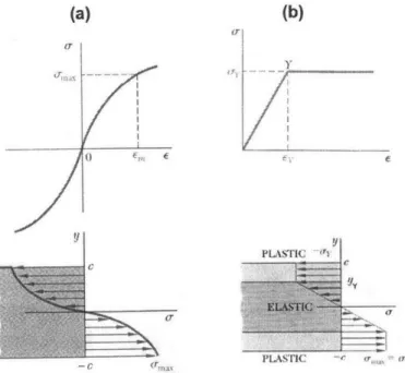
V(x)dx = Mt + (Lh - x) Ft (2.3) where Lh is the length of the hinge. Figure 2-4 illustrates the internal shear force and bending moment distribution along the hinge. The moment diagram suggests that, under the assump-tions that the hinge is made of a homogeneous material and has a uniform cross-sectional area, the hinge section subject to the largest bending moment is at its base.Analysis of beam bending is very common in structural mechanics, and the failure mecha-nism of ductile metals is a well understood process too. The internal moment in the gold hinge induces a linear axial strain distribution across the beam thickness that varies from tensile (positive) in the lower section of the beam to compressive (negative) in its upper section. By virtue of symmetry, the unstrained neutral axis for a hinge with a rectangular cross section is at its center axis (Figure 2-5).
Taking a look at the stress versus strain diagram of gold (Figure 2-6) [RR], we distinguish between two regimes: elastic and plastic. The transition point between the two regimes is at the yield stress ay, which, for ductile material, is determined by drawing a line parallel to the
Lh -Mt v
Ft
C1~ .I.
Lh M M + LtMt
LhFigure 2-4: Internal shear force and bending moment distributions for the hinge subject to a tip force and moment
f
C lt"
Figure 2-5: Linear strain distribution profile in a beam with rectangular section subject to a bending moment
Elastic Plastic
Figure 2-6: Stress strain diagram of gold (typical of a ductile material). The yield stress is determined by the offset method; drawing a line parrallel to the linear section with a 0.002 strain-axis intercept.
Figure 2-7: Linear stress distribution across the thickness of a beam (a) before yielding and (b) at the onset of plastic deformation
linear section of the plot through the 0.2% strain point.
In the elastic range, the stress is directly proportional to the strain (a = EE), so the stress distribution in the beam section is also linear (Figure 2-7). At equilibrium, the magnitude of the maximum stresses, at the top/bottom, is
Umax = MC (2.4)
where c is distance from the neutral axis to the top/bottom of the beam, and I is the area moment of inertia of the section (for a rectangular beam of thickness 2c and width b, I =
surfaces to 0 at the neutral axis, so, at a distance y from the neutral axis, the axial stress is given by
My
(2.5) o(y)
and the radius of curvature of the beam is
El 2Ebc3
3M (2.6)
M 3M
where E is the Young's modulus of elasticity of the material.
We define the yield internal moment My as the moment required to initiate yielding in a beam section. Rearranging the terms of Eq. 2.4, My can be calculated as
My I 2bc2ay. (2.7)
c 3
Any section of the beam subject to a bending moment larger than My will start to deform plastically. Assuming material continuity, the strain profile is independent of whether the stress in the material is in the elastic regime or the plastic regime. It continues to be linear; however, the stress distribution is linear only in the elastic range. The profile of the stress versus strain curve of the material, including the non-linear plastic part, needs to be taken into account. Figure 2-8a shows the stress distribution for a generic ductile material in plastic deformation. A common simplification is to assume that the metal is perfectly elastic in the first phase and fails in a perfectly-plastic manner, as shown in the stress vs. strain curve of Figure 2-8b. The stress profile in the beam section is, hence, trapezoidal, where the stress in the top and bottom sections saturates at ay in the plastic regime. As we increase the moment beyond My, the thickness of the elastic core decreases while that of the plastic sections increases. Equating the moment of the stresses to the applied moment at the section gives
M() = 2 y y dy + 2 y (y) dy
b JkyY}Y+Y~~Y
= c2c.y 1 - y ). (2.8)
(a)
... .. . . . ... .... (b)In
s-i
N;IJFigure 2-8: Stress distribution along the thickness of a hinge made up of (a) a generic ductile metal and (b) an idealized elastoplastic metal
deformation. The strain gradient can be calculated from the slope of the stress in the elastic core section
'-(y)core = (y)E = _ (2.9)
yY
the radius of curvature is thus
P y Eyy (2.10)
Combining Eq.s 2.8 and 2.10 relates the radius of curvature of the beam to the bending moment at a particular section
M(X) = c2. ( ( - (cTyp) 2) (2.11)
rearranging the terms of Eq. 2.11
= [ 1 - J .bc2 (2.12)
Eq.s 2.3, 2.6 and 2.12 determine the profile of the gold hinges for any tip loading condition. The deflection angle of the tip of the hinge 0, which is equal to the angle of the folded segment, can be calculated by integrating the angles of small beam sections along the length of the hinge
dOx _ 1 (2.13) dx P(X) cos where 1/3E - 1/2 0 < X < xy PL\ = M (2.14) -E- xy < x < Ls
and xy is the transition point between the elastically and plastically deformed sections of the hinge.
In theory, the applied force can be in any direction as dictated by the cross product of the unit vectors of the external magnetic field and the current in the wire loop. To simplify the experimental procedures, we assume that the applied field is kept at a fixed angle, hence the actuation force is at a fixed angle OF (measured from the vertical). Based on that, the moment it exerts on the hinge, Mt, and the transverse component of the force, F, vary as the hinge deforms significantly, as depicted in Figure 2-9. At a folded angular position 0, the moment
... ...
...
MtL
Figure 2-9: Diagram of a folded segment subject to a tip force F at an angle OF from the vertical, at a deflection angle of 0.
and transverse force at the tip of the hinge are given by
Mt = FL, cos(0 - OF) (2.15)
Ft = F cos(O - OF) (2.16)
The bending moment distribution is then
M(,o) = F cos(9 - OF) (Ls - Lh - x) (2.17)
By setting
M = My = 2bc2oy, (2.18)
3
the point of transition between elastic and plastic deformation, xy, is
2bc~gy
xy = L,, + Lh -ca (2.19)
3F cos(O - OF)
Eq. 2.17 shows that the moment distribution along the hinge is a function of the hinge's tip deflection angle itself. However, the moment distribution determines the curvature of the beam, which, itself, defines the tip angle. The dependence is also nonlinear, so, to find the
UY 220MPa
E 55GPa
v 0.44
G 27GPa
Table 2.1: Material properties for gold
deflection angle 0 due to a force F, one needs to simultaneously solve Eq.s 2.13, 2.14 and 2.17 numerically.
2.3
Numerical Simulations of Rectangular Hinges
MATLAB was used to solve the equations numerically. The MATLAB scripts are included in Appendix C for reference, and Table 2.1 lists the material properties of gold used in the simulations .
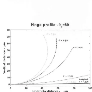
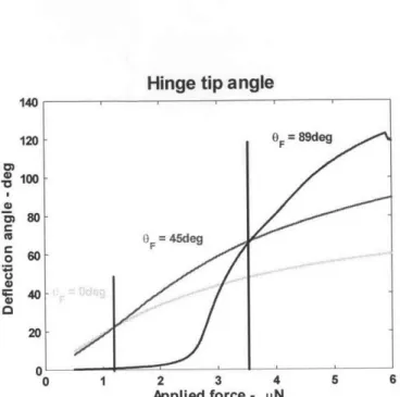
Figure 2-10 is a plot of the applied force vs. tip deflection angle of a 600nm thick hinge that is 300pm wide and 100pm long. The force is applied vertically at the end of the folded membrane, whose length is assumed to be
1mm,
and its magnitude and direction are maintained constant throughout the fold. As the hinge angle increases, the moment arm and the transverse component of the force both decrease. They are maximum in the starting flat configuration, which explains the rapid rise in the angle for small deflections. The tip angle then saturates at around 750 with a force of 14.5pN. The sharp drop in the curve at that point occurs because the bending moment at the base of the hinge is high enough to plastically deform the whole beam section. The radius of the elastic core, in the elasto-plastic model goes to zero, and the trapezoidal stress profile shown in Figure 2-8 becomes a rectangle. The radius of curvature at that section, given by equation 2.14, becomes imaginary, and the simulation terminates. The slope of the graph is a measure of the effective compliance of the hinge; the hinge starts out as being very compliant, and it becomes stiffer with increasing 0.This saturation effect is evident in the moment distribution and hinge profile plots as well. In Figure 2-11, the shift in the moment curves for a constant increment of the applied force decreases with the increasing value of that force. For a force of 14.40IN, part of the hinge, that is closer to the base (~30pm in length), starts to deform perfectly plastically. Shortly after