HAL Id: hal-03032166
https://hal.archives-ouvertes.fr/hal-03032166
Submitted on 30 Nov 2020
HAL is a multi-disciplinary open access
archive for the deposit and dissemination of
sci-entific research documents, whether they are
pub-lished or not. The documents may come from
teaching and research institutions in France or
abroad, or from public or private research centers.
L’archive ouverte pluridisciplinaire HAL, est
destinée au dépôt et à la diffusion de documents
scientifiques de niveau recherche, publiés ou non,
émanant des établissements d’enseignement et de
recherche français ou étrangers, des laboratoires
publics ou privés.
Field and charge distribution at semicon/polyethylene
interfaces from combinations of probe force microscopy
measurements
Francesco Gullo, T Christen, Christina Villeneuve-Faure, H Hillborg,
Christian Laurent, Séverine Le Roy, G. Teyssedre
To cite this version:
Francesco Gullo, T Christen, Christina Villeneuve-Faure, H Hillborg, Christian Laurent, et al.. Field
and charge distribution at semicon/polyethylene interfaces from combinations of probe force
mi-croscopy measurements. 16th Int. Symp. on Electrets (ISE), Leuven, Belgium, 4-8 Sept. 2017,
Sep 2017, Leuven, Belgium. p.29. �hal-03032166�
Field and charge distribution at semicon/polyethylene interfaces
from combinations of probe force microscopy measurements
F. Gullo1, T. Christen2, C. Villeneuve-Faure1, H. Hillborg3, C. Laurent1, S. Le Roy1, G. Teyssedre1
gullo@laplace.univ-tlse.fr
1 LAPLACE, Université de Toulouse, CNRS, INPT, UPS, France 2 ABB Corporate Research, Baden, Switzerland
3 ABB Corporate Research, Vasteras, Sweden
Abstract: Two modes of Atomic Force Microscopy, namely the Peak Force – Quantitative Nano Mechanics and the Kelvin Probe Force Microscopy, are used for the nanoscale characterization of semicon(SC)-polyethylene(PE) interfaces in a SC-PE-SC-sandwich. A combination of the two methods provides physical (local geometry, roughness) and electrical (electric field, space charge) properties.
Keywords: HVDC insulation, space charge, semicon-contact, AFM, KPFM, polyethylene
Introduction
To understand electrical conduction mechanisms in polymer insulation is crucial for high voltage direct current (HVDC) applications, particularly for the prediction and control of the field distribution. Dielectric polymers exhibit properties which aggravate a sound physical understanding of bulk conductivity: amorphous or semi-crystalline structure, small intrinsic carrier density, low-mobility states and carrier traps, charge carrier injection etc.. In this contribution, we focus on the electrode contact, which is relevant because (1) the contact properties can strongly determine the electrical conductance behaviour of the insulation, e.g. due to injection of majority carriers in combination with the smallness of intrinsic carrier density, and (2) the calculation of electric fields based on drift-diffusion models requires realistic boundary conditions at the contacts [1]. In this work, we consider a typical prototype interface, as ubiquitous in HV equipment, between a carbon black (CB) filled host polymer (‘semicon’, SC) and the insulating pure host polymer (polyethylene, PE). The fundamental processes which govern the contact physics and their dependence on the microstructure properties in such systems are still poorly understood [2]. We report on results on the application of Peak Force - Quantitative Nano Mechanics (PF-QNM) and Kelvin Probe Force Microscopy (KPFM) techniques [3] to the SC/PE interface in a SC/PE/SC sandwich structure. Results and Discussion
The geometrical interface was characterized by measuring the adhesion force with PF-QNM. This parameter shows a contrast between CB dots and the PE matrix, and provides the CB-induced interface roughness. Electrical properties were characterized by measuring the surface potential with KPFM. The determination of the charge distribution requires the solution of Poisson’s equation, V= -free-pol,
where the free and polarization charges need to be
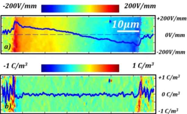
considered with special care on the nanoscale in this strongly nonuniform and anisotropic system. Also the spatial derivatives on experimental and thus noisy data needs a special treatment. We use the Savitzky-Golay method which fits locally a polynomial function such that the derivatives can be performed analytically. In figure 1, resulting E-field (first derivatives) and space charge (second derivatives) distributions are shown for a specific case. Charges appear close to the SC/PE interface (few microns) with negative charge in PE and positive charge in SC.
Figure 1: a) Electric field and b) charge density for a 50µm thick SC/PE/SC structure. Blue curve: profile along the dotted line.
Conclusions
KPFM and PF-QNM measurements allows us to characterize the SC/PE interface roughness and the contact charge density. Our approach will allow to determine the boundary conditions for field simulations and to gain new insight into physical phenomena at the electrode interface.
References
[1] T. Christen, IEEE Trans. Dielectr. Electr. Insul. 2015,
22, 35; (ibid) 2016, 23, 3712.
[2] G. Teyssedre, C. Laurent, IEEE Trans. Dielectr.
Electr. Insul. 2005, 12, 857.