Chip-scale modeling of pattern dependencies in copper chemical mechanical polishing processes
Texte intégral
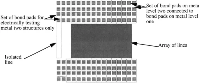
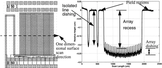
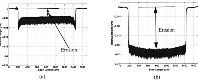
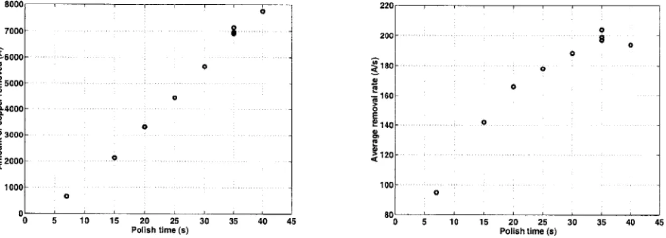
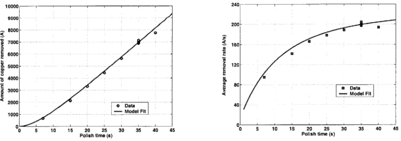
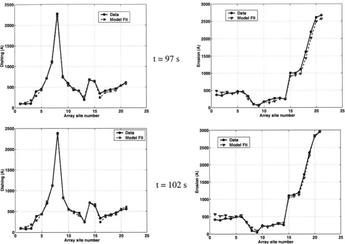
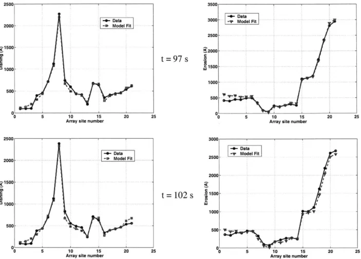
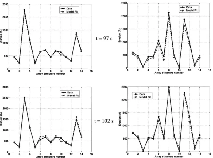
Figure
Documents relatifs
Here, we report for the first time to our knowledge, in a cohort of grade II/III gliomas excluding GBM, a 22 gene predictor which allows an early identification of poor
Badiou, qu’il s’agit l` a ` a la fois d’un fragment fini, parfaitement circonscrit et analysable sur archives de l’histoire des math´ ematiques (de Galois ` a Artin), mais
COMPARATIVE STUDY OF MERCURY AND CADMIUM EXPOSURE IN A FRESHWATER FISH (BRACHYDANIO RERIO) Histological microanalysis of Cd-induced minerai
However, Liljedahl et al (1984) dealing with 2 populations of laying hens reported a positive trend in genetic variation with age for various egg production
However, if a reservoir with a large area and an irregular well pattern (some areas have a large well pattern density, and other areas have a small well pattern density), it is dif
b production asymmetry and the muon, kaon, and pion detection asymmetries using LHCb data exist [5, 8–10], and estimates of the proton detection asymmetry using simulated events
sequences using affine gap costs, the time complexity of finding optimal alignments using concave gap costs, and the random permutation of a sequence preserving its
of Atomic Energy Government of India (DAE), Department of Science and Technology, Government of India (DST), University Grants Commission, Government of India (UGC) and Council
