Charge, Spin and Pseudospin in Graphene
by
Dmitry A. Abanin
Submitted to the Department of Physics
in partial fulfillment of the requirements for the degree of
Doctor of Philosophy
at the
MASSACHUSETTS INSTITUTE OF TECHNOLOGY
September 2008
@ Massachusetts Institute of Technology 2008. All rights reserved.
Author ...
Department of Physics
August 5, 2008
C ertified by ... ....
Leonid S. Levitov
Professor of Physics
Thesis Supervisor
Accepted by ...
Associate
-7 Ad4
ZI
lfhomaf. Greytak
Department Head
f Education
ARCHIVES
MASSACHKcMr S IN. rJTUT
oL
R
1 :.
9
Charge, Spin and Pseudospin in Graphene
by
Dmitry A. Abanin
Submitted to the Department of Physics on August 5, 2008, in partial fulfillment of the
requirements for the degree of Doctor of Philosophy
Abstract
Graphene, a one-atom-thick form of carbon, has emerged in the last few years as a fertile electron system, highly promising for both fundamental research and appli-cations. In this thesis we consider several topics in electronic and spin properties of graphene, with a particular emphasis on the quantum Hall effect (QHE) regime, where this material exhibits most interesting behavior.
We shall start with analyzing general properties of the two-terminal conductance for graphene mono- and bilayer samples. Using conformal invariance and the theory of conformal mappings, we characterize the dependence of conductance on the sam-ple shape. We identify the features which distinguish monolayers and bilayers and illustrate the use of the two-terminal conductance as a tool for sample diagnostic.
Next, we present a microscopic study of the edge states in the QHE regime. This analysis provides a simple and general explanation of the half-integer Hall quantiza-tion in graphene. We discuss the edge states dispersion for different orientaquantiza-tions of the boundary, and propose a way to image the edge states using STM spectroscopy.
Then, we extend the picture of edge states to describe QHE in spatially nonuniform systems, recently demonstrated p-n and p-n-p devices. We show that the bipolar p-n and p-n-p junctions can host counter-circulating QHE edge states, which mix at the
p-n interfaces, giving rise to fractional and integer quantization of the two-terminal
conductance, observed in this structures.
Graphene exhibits interesting spin- and valley-polarized QH ferromagnetic (FM) states. We show that spin-polarized QH state at zero doping hosts counter-circulating edge states carrying opposite spins, and propose to use this regime as a vehicle to study spin transport.
We study ordering in the valley-polarized QH state. Coupling of valley QHFM order parameter to random strain-induced vector potential yields an easy-plane-type ordering of the valley QHFM, giving rise to Berezinskii-Kosterlitz-Thouless transition, with fractionally charged vortices (merons) in the ordered state.
Thesis Supervisor: Leonid S. Levitov Title: Professor of Physics
Acknowledgments
First and foremost I would like to thank my advisor, Leonid Levitov, who to a large extent determined the direction of the research presented in this thesis. His enthu-siasm and remarkable breadth of knowledge make Leonid a great advisor and a real
pleasure to work with. I find Leonid's way of thinking about physics to be insightful and elegant. With his ability to see phenomena at many different angles, an unlimited curiosity, a keen eye for an interesting problem and an impressive arsenal of mathe-matical skills, Leonid is a consummate theoretical physicist. I was very lucky to be his student, and he remains a role model for me.
Throughout my years at MIT, Leonid has brought various research topics to my attention, suggested an endless number of problems to work on, and helped me with solving some of them. I thank him for that. However, what I appreciate even more is that Leonid has been my mentor. Many hours of our discussions has largely shaped me as a scientist and made me understand, to a certain degree, how to do research on my own. He has been supportive, attentive, kind, and, maybe even more importantly, patient, which has made the learning process at MIT easy and enjoyable for me.
Another theorist who had a great influence on my development, as well as on this thesis, is Patrick Lee. Working with him was a privilege for me. Patrick has a remarkable physical intuition and an exceptional clarity of thinking; he is quick to find a clear and qualitative explanation for any physical phenomenon, no matter how complicated it may seem. I am very thankful to Patrick for sharing his skills; interacting with him helped me to see physics from a new perspective. Another Patrick's quality that I very much appreciate is his modesty. Despite being famous, he is always approachable, easy to talk to, and open to new ideas.
Experiment and theory in physics always go hand in hand. During my years at MIT I was lucky to interact with many outstanding experimentalists, who kindly shared their findings and made an effort to understand our theories. In fact, approx-imately half of what is presented below is the result of collaboration with experimen-talists.
I owe a great deal of what I know about experiment to Charlie Marcus, as well as his former and current students, Dominik Zumbuhl, Leo DiCarlo, and especially Jimmy Williams. A meeting at MarcusLab would always be an opportunity to learn about exciting experimental results, get lots of questions and ideas, and drink ex-cellent espresso. Working with Charlie and his students, and being exposed to their
energy, optimism, great feel for physics, and hilarious sense of humous, has been a
joy for me.
It was a tremendous privilege for me to collaborate with Andre Geim's group
and Philip Kim's group. Andre's group discovered graphene; Andre's and Philip's groups discovered most of what we currently know about graphene properties. Andre and Philip gave me an opportunity to learn about experiments which will surely
become classic; without them this thesis would be completely different. I am thankful to Andre and Philip, as well as their former postdocs, Kostya Novoselov, Barbaros
Ozyilmaz, and especially Pablo Jarillo-Herrero.
I am thankful to the members of MIT Condensed Matter Theory Group for their genuine interest in physics, eagerness to discuss any topic any time, and creating a
scientific environment that I consider to be nearly ideal. Conversations with Maxim
Vavilov, Markus Kindermann, Saeed Saremi, Michael Slutsky, Nan Gu, Maissam Barkeshi, and Senthil Todadri were motivating and insightful for me.
I am especially grateful to my officemates - Pouyan Ghaemi, Roman Barankov and Mark Rudner - people with whom I spent a large fraction of every day. Pouyan, Roman and Mark are very different from each other, yet all of them are remarkable
people and physicists; they are also dear friends to me. Pouyan is a very light-hearted person; talking to him is always easy and enjoyable. Roman's sincere passion for truth continues to inspire me and helps me to be honest with myself. Mark is truly one of the kindest people whom I know; his optimism and positive energy made an atmosphere in our office friendly and productive. Special thanks are due to Mark for helping me to improve my presentation skills, and correcting an endless number of articles in this Thesis.
prac-ticing dancing. Just a hobby at first, dancing gradually became an important part of my life, which taught me most of what I know about human body and emotions. My dance coach, Armin Kappacher, has been very much like a life mentor for me. Armin knows everything there is to know about the mechanics of human movement; he brings with him a tremendous energy, love of life, and utmost common sense. I thank him for sharing all of that; I am glad I could learn so much from him. I am also thankful to my dance friends, Olga Rostapshova, Andriy Didovyk, Esya Volchek, Ran Yi, Henry Newman, Rob Lakow, Jimmy Vanzo, Muyiwa Ogunika, Katya Kukuruza, Sarah Tishler, and many others; being around them was always fun, and helped me stay in a positive mindset.
I thank my closets friends, Vova Manucharyan, Adilet Imambekov and Zhao Chen for always being there for me; they are just like family to me. I know Zhao, Adilet and Vova very well, yet being around them is always exciting. I am grateful to Zhao for her kindness and understanding; thinking of Adilet and his jokes always makes me smile; Vova's encouragement and advice throughout some of the toughest periods of my life have been invaluable. Thank you, for all your support, for making me happy, and just for being the way you are.
I am grateful to my parents for their constant support, teaching me by example, confidence in me, and all their love. I also thank my sister Dasha, as well as the rest of my family. Every moment spent with them is a memorable experience which helps me see things from a broader perspective, teaches me something valuable, and just gives me a chance to feel at home.
Contents
1 Introduction
1.1 Graphene: structural properties . . . . 1.2 Electronic properties of graphene . . . .
1.3 Introduction to the Quantum Hall Effect . . . . 1.3.1 Edge states and the QHE. ...
1.3.2 Quantum Hall ferromagnetism ... . . . .
1.4 QHE in graphene ...
1.4.1 Half-integer QHE ...
1.4.2 Spin- and valley-split QHE states . . . . 1.4.3 Other directions ...
1.5 Main results of this thesis ...
1.5.1 Conformal invariance, shape-dependent conductance and
sample characterization ...
1.5.2 Edge states and the half-integer QHE . . . . 1.5.3 QHE in locally gated graphene devices . . . .
1.5.4 Spin and charge transport at the graphene edge . . . . 1.5.5 Disorder-induced anisotropy in valley QH ferromagnet
27 31 34 39 39 43 46 46 49 54 graphene ... . 55 S. . . 56 S. . . 57 S. . . 58 S. . . 59
2 Conformal Invariance and Shape-Dependent Conductance of Graphene
Samples 61
2.1 A bstract . . . .. . 61
2.2 Introduction ... ... 62 2.3 Duality relation for conductance ... .. 63
2.4 The semicircle model ...
2.5 Conformal mapping approach . . . ...
2.6 Conductance fluctuations in small samples . . . . 2.7 Rectangle as the mother of all shapes; conformal invariance and
uni-versality . . . . 2.8 Conclusions . . . .
3 Two-Terminal Conductance of Graphene Devices Hall Regime
3.1 Abstract . . . .
3.2 Introduction ...
3.3 Conductance of single-layer graphene samples . . .
3.4 Conductance of bilayer graphene samples . . . .
3.5 Non-rectangular samples . . . .
3.6 Summary and discussion . . . .
4 Edge States and the Half-Integer Quantum Hall Effect
4.1 A bstract . . . .
4.2 Introduction and Outline ...
4.3 Edge states spectrum . ...
4.3.1 Armchair edge. ...
4.3.2 Zigzag edge. ...
4.4 STM spectroscopy of edge states.
. . . . 98 . . . . 101
. . . . . 106
5 Quantum Hall Effect in Locally Gated Graphene Devices
5.1 A bstract . . . .
5.2 Introduction .. ... . . .. . ... . .. .. . . . . .. ... 5.3 Conductance quantization in p-n junctions . . . .
5.4 Mixing mechanisms and shot noise . . . . .
5.5 Conductance quantization in p-n-p junctions . . . . 5.6 Stability of the QHE in p-n-p junctions . . . .
in the Quantum 81 81 81 83 88 90 94 97 . . . . 97 . . . . 97 . . . . 98 109 109 110 113 116 121 125
6 Spin and Charge Transport near the Dirac Point 135
6.1 Abstract . . . 135
6.2 Introduction and outline ... 136
6.3 Spin polarization versus valley polarization . ... 138
6.4 Spin transport properties ... . .. ... . 141
6.5 Dissipative QHE ... 145
7 Order from Disorder in Graphene Quantum Hall Ferromagnet 153 7.1 Abstract .. . . . .. . . .. . . . .. . 153
7.2 Introduction ... 153
7.3 Random vector potential and valley anisotropy . ... 157
7.4 Summ ary ... ... 162
8 Summary and outlook 163 8.1 Sum m ary ... ... 163
List of Figures
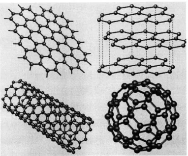
1-1 Graphene (upper left) as a mother of carbon allotropes. Graphite (up-per right) is obtained by stacking graphene planes on top of each other.
Carbon nanotubes (lower left) are rolled-up graphene sheets, and buck-yballs (lower right) are obtained by substituting some hexagons in
graphene lattice by pentagons, which gives rise to a curvature and results in graphene curling into a sphere. From Ref. [1]. ... 32
1-2 (a) Graphene lattice with armchair and zigzag edges. (b) Graphene hexagonal Brillouin zone. K and K' are the two non-equivalent Bril-louin zone corners, where energy gap vanishes. (c) Our choice of two linearly independent zero-energy Bloch functions for the K point. Here
7 = e2ni/3. The zero-energy Bloch functions for the K' point are
ob-tained from those for the K point by complex conjugation. ... . 36
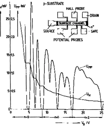
1-3 The Hall (py) and longitudinal (p,,) resistivity of a two-dimenional electron gas as a function of gate voltage, plotted in units of the voltage
on Hall probes (UH) and potential probes (Upp). Resistivity Pxy exhibits a series of quantized plateaus with values py = h/ne2 - a remarkable
phenomenon known as quantum Hall effect. Inset: schematic of the device. From the paper by von Klitzing [2] . ... 40
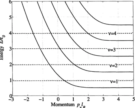
1-4 Spectrum of the Landau levels in a strip (in units of Eo = hw,),
ob-tained by numerically solving the Schroedinger equation with a hard-wall boundary condition. Momentum py, equivalent to the magnetic oscillator position, is used to classify the energy levels. Landau lev-els, which are flat in the bulk, acquire dispersion near the edge. This corresponds to one-dimensional channels (one per LL) localized near the edge and propagating with velocity v = d-n/dpy. At integer
fill-ings, v = n, there are n conducting edge channels, which give rise to
quantized Hall conductivity of ne2/h. . ... 42 1-5 Quantum Hall effect in graphene at B = 14 T. Transport coefficients,
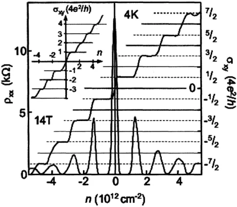
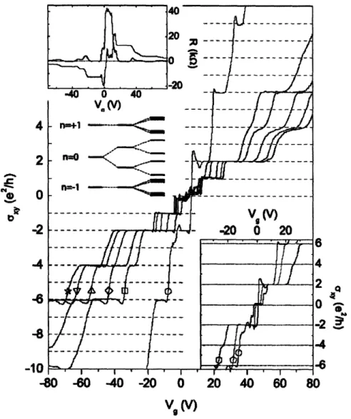
Hall conductivity ao, (red) and longitudinal resistivity P,, (green), are shown as a function of the carrier density. The Hall conductivity ex-hibits half-integer quantization in units of 4e2/h, resulting from the Dirac spectrum of excitations in graphene. Inset: a,y as a function of
carrier density in bilayer graphene. The massive electron-hole symmet-ric band structure of bilayer graphene gives rise to the quantization of
the Hall conductivity at integer values [3]. From Ref. [4] ... 48
1-6 Evolution of the Hall conductivity ay as a function of gate voltage V, with increasing magnetic field: 9 T (circle), 25 T (square), 30 T
(diamond), 37 T (up triangle), 42 T (down triangle), and 45 T (star).
Right inset: detailed behavior of a,y near the Dirac point for B = 9 T (circle), 11.5 T (pentagon) and 17.5 T(hexagon). Left upper inset: longitudinal and Hall resistivity measured at B = 25 T. Left lower inset: a schematic drawing of the LL splitting in high magnetic fields. From Ref. [5] . ... .. . 52
1-7 Longitudinal and Hall conductivities a,, and a., (a) calculated from
PXX and pxy measured at 4 K and B = 30 T (b). The upper inset shows one of the measured devices. Temperature and magnetic field dependence of Pxx at v = 0 are shown in the insets below. Note the
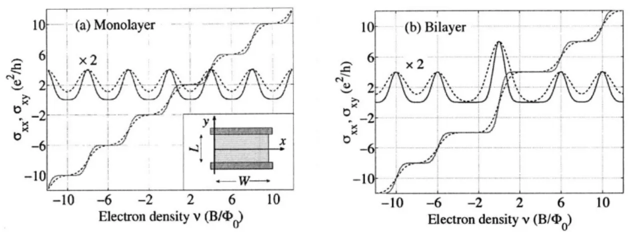
2-1 Longitudinal and Hall conductivity for (a) graphene monolayer and (b) graphene bilayer, obtained from the semicircle model, Eqs.(2.9),(2.7),(2.8), for two values of the Landau level width parameter A = 1.7 (solid lines),
A = 0.5 (dashed lines). Inset: Schematic of a conducting sample of di-mensions L and W, of a rectangular shape, with source and drain at opposite sides ... 65
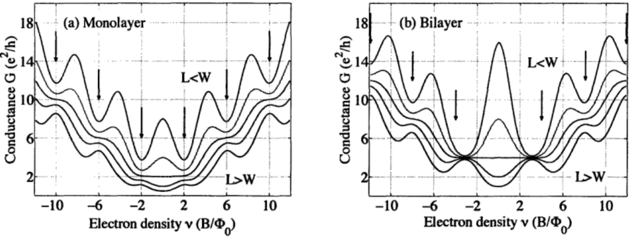
2-2 Two-terminal conductance (2.15) of a rectangular graphene sample: (a) monolayer, (b) bilayer, for aspect ratios L/W = 0.25,0.5, 1,2,4 (top to bottom) with the Landau level width parameter A = 1.7 (cor-responding to solid lines in Fig.2-1). Arrows mark the incompressible densities (2.5), (2.6). Note the plateau at v = 0 for the square case,
L = W (red curve), which is in agreement with the behavior predicted
by Eq.(2.1). ... 68
2-3 Same as in Fig.2-2 for broader Landau levels, described by (2.8) with
A = 0.5 (dashed lines in Fig.2-1); the sample aspect ratios are L/W =
0.25, 0.5, 1, 2, 4 (top to bottom). Note that the qualitative features, such as the positions of the conductance minima at the QHE plateau centers for L < W (maxima for L > W), as well as the conductance
values at these densities, are similar to those seen in Fig.2-2 despite increased Landau level broadening. Note also the relative size of the
v = 0 peak in the monolayer and bilayer cases, compared to the size
of neighboring peaks at other compressible densities, which is also in-sensitive to the Landau level broadening. . ... . 69
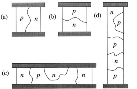
2-4 Examples of possible p-type and n-type puddle configurations near
graphene charge neutrality point for mesoscopic samples with at least one of the dimensions comparable to the typical puddle size (. In (a)
and (b) two possible configurations are shown for a square sample with
L, W ( ý. The corresponding conductance values, G = 4e2/h for (a)
and G = e2/h for (b), are different from the value G* = 2e2/h predicted
by the effective medium (semicircle) model. Puddle arrangement in a
short and wide sample (L < ( < W) and in a narrow and long sample
(W
5<
< L) is illustrated in (c) and (d). . ... 722-5 Conformal invariance illustrated by several conducting domains with contacts. If two domains can be conformally mapped on each other
so that the contact regions are mapped on the corresponding contact regions, their conductances are the same. The Riemann mapping
the-orem guarantees existence of a mapping between an arbitrary domain (a) and a unit disk (b) such that three points on the boundary of (a), marked 1, 2 and 3, are mapped on any three points (1, 2 and 3) on the circle (b). The position of the fourth point, which is not specified, defines a one-parameter family of possible conduction problems. All such problems can be parameterized by rectangles (c) with different aspect ratios. ... ... .. 76
2-6 Complex halfplane and conduction problem in it, which can be mapped on that in a rectangle using the Schwartz-Christoffel mapping, Eq. (2.23). The aspect ratio L/W of the equivalent rectangle depends on the rela-tive size of the contacts, shown in blue, and the distance between them. The end points of the contacts are p1,2 = T1, 63,4 = -1/k. . . . . . . 78
3-1 Theoretical density-dependent two-terminal QH conductance g as a function of carrier density obtained using Ref. [7] (see text for details) shown for (a) single-layer graphene; (b) gapless bilayer graphene, and (c) gapped bilayer graphene. Black and red curves correspond to aspect ratios ýe = L/W = 2 and 0.5. Local extrema of g at filling factors
v = +2, +6, +10.. for single layers and at v = +4, +8, +12.. for bilayers are either all maxima (ýe < 1) or all minima (e, > 1). In (a) and (b), the local extremum at v = 0 is of opposite character (i.e., mimimum for ~ < 1 and maximum for , > 1). In (c), due to the gap, g vanishes at v = 0 regardless of geometry. ... 84
3-2 (a) Inset: Conductance g in the quantum Hall regime as a function of
B and Vbg at T=250mK for sample Al. Black dashed lines correspond
to filling factors of -6, -10, -14, -18 and align with the local maxima of conductance. Main: (black) Horizontal cut of inset giving g(Vbg)
at B=8T and (red) calculated g (e = 1.67 and A = 1.2). (b) Inset: Conductance g in the quantum Hall regime as a function of B and
Vbg at T=250mK for sample A2. Black dashed lines correspond to filling factors of -6, -10, -14, -18 and align with the local minima of conductance. Main: (black) Horizontal cut of inset giving g(Vbg) at
B=8T and (red) calculated g (ce = 0.2 and A = 1.2). . ... 86
3-3 Inset: Measured g of sample B1 as a function of B and Vbg at T = 4K.
Black dashed lines, corresponding to v= -12, -16, -20, align with local
minima of g. No minima are observed at v = 8 for 5T < B < 8T. Main: Horizontal cut of inset at B = 8T (black), and calculated g (red) using A = 0.7 and effective aspect ratio e = 0.8 (solid) and ýe =
3-4 Measured g(Vbg) for sample B2 (black) and the calculated conductance for ýe = 0.29 and A = 0.25 (red). Two key features in the curve suggest this sample is a gapless bilayer, namely, a pronounced peak in g near the CNP, and the larger spacing between the two minima straddling
the CNP compared to the spacing A - 9.5 between other consecutive minima. ... 89
3-5 g(Vb,) for sample C (black) and the calculated conductance (red) for the best-fit value of ýe = 0.83 (A = 0.7). The observed conductance (black) can be reproduced by conformally mapping the asymmetric contact configuration into a rectangular shape (see inset), which for
this device results in an equivalent rectangle of ýe = 0.9. . ... 91 3-6 A polygon representing sample C (see Fig. 3-5). Blue regions
corre-spond to contacts, length scale a = 200 nm. . ... 93 3-7 Mapping of the polygon in Fig. 3-6 (sample C) onto the upper
half-plane (shown not to scale). Blue lines correspond to contacts. First, we replace the rectangle in Fig. 3-6 by a half-infinite strip, extend-ing indefinitely to the right. Next, we map the domain shown in (a)
onto a rectangle with contact 3-5-6-4 straightened out (b). Under this mapping, the sample is slightly distorted, as indicated by the yellow polygon in (b). Because the deviation of the yellow polygon's bound-ary from the original sample's boundbound-ary (red line in (b)) is fairly small, it can be neglected, giving a half-infinite strip (c). Finally, the domain (c) is mapped onto the upper half-plane (d), which allows to find the cross ratio A1234 and evaluate the effective aspect ratio (see text). . . 93
4-1 Graphene energy spectrum near the armchair boundary obtained from Dirac model, Eq.(1.1). The boundary condition, Eq.(4.8), lifts the K,
K' degeneracy. The odd integer numbers of edge modes lead to the
4-2 Graphene energy spectrum near the zigzag boundary obtained from Dirac model, Eq.(4.12), with boundary condition (4.13). (a) Spectrum
for the K valley. The zeroth LL transforms into dispersionless surface mode near the edge. (b) Spectrum for the K' valley. The zeroth LL
mixes with the surface mode at the edge, giving rise to two branches of dispersing QH edge states. ... 103
4-3 Landau levels spectrum of a graphene strip with zigzag edges, obtained numerically in the framework of the tight-binding model [8]. The in-terplay between the zeroth LL and surface state near the edges is illus-trated. The zeroth LL in the K valley (left) transforms into a surface state near the right strip edge; the surface state traverses through the whole Brillouin zone, and mixes with the K' zeroth LL, generating a pair of quantum Hall edge states. The surface states, despite being dispersive owing to the next-nearest neighbor hopping introduced in the model, localize due to the coupling to strong edge disorder and do not contribute to the transport properties. Thus the half-integer quantization is preserved for the zigzag case. Adopted from Ref. [8] . 104 4-4 STM spectrum of graphene near the zigzag edge for sublattice A (a)
and B (b). x is the distance to the edge. Due to the momentum-position duality, analysis of the STM spectrum allows extraction of the edge states dispersion. ... .. 107
5-1 Conductance of a graphene p-n junction in the QHE regime, from Ref. [9]. (a) schematic of the device, with a local top gate used to create a p-n junction. (b) Conductance map as a function of top and bottom gate voltages. (c), (d) conductance as a function of top gate voltage at fixed filling factors (6 and 2, respectively) in the non-gated region. Conductance exhibits a series of quantized plateaus with fractional and integer values ... . ... . 111
5-2 Schematic of QHE edge states for (a) bipolar regime of pn junction, and (b) unipolar regime of nn and pp junctions. In case (a) the edge states counter-circulate in the n and p regions, bringing to the pn interface electrons and holes from different reservoirs. Mode mixing at the interface leads to the two-terminal conductance (5.1). In case (b), since the edge states circulate in the same direction without mixing at the interface, conductance is determined by the modes permeating the
whole system, g
=
min(Ivli, Jv
2)
...
114
5-3 Two-terminal conductance vs. gate voltage, given by Eq. 5.2 in the unipolar case (v1,2 of equal sign), and by Eq. 5.1 in the bipolar case vl > 0, v2 < 0. The boundaries of QHE regions are specified by v1,2 = 0, 14,
+8...,
with the gate voltage dependence of v1,2 given by Eq. 5.3.Parameters used: distances to the top and back gates h = 30 nm,
d = 300 nm, magnetic length iB = 10 nm, dielectric constant n = 3. . 114
5-4 Shot noise Fano factor, Eq. (5.8), plotted vs. gate voltages for the same parameter values as in Fig.5-3. Noise is zero in the unipolar regime (pp
or nn) due the absence of current partition at the junction interface, but finite in the bipolar regime due to edge mode mixing at the pn interface. ... 119
5-5 Edge states (a) to (c) and the quantized conductance values in a p-n-p junction (d). (a) to (c): different edge states diagrams representing
possible equilibration processes taking place at different charge densi-ties in the GLs and LGR. The purple region indicates the LGR, yellow boxes indicate contact electrodes. (d) Simulated color map of the the-oretical conductance plateaus expected from the mechanisms shown in (a)-(c) for different filling factors in the GLs and LGR. The numbers in the rhombi indicate the conductance at the plateau. . ... 122
5-6 (a) Color map of conductance as a function of top and back gate
volt-ages at magnetic field B = 13 T and T = 4.2 K. The black cross indicates the location of filling factor zero in LGR and GLs. Inset:
Conductance at zero B in the same range of gate voltages and the same color map as the main figure (white denotes g > 10.5e2/h). (b)
g(Vt) extracted from (a), red trace, showing fractional values of the
conductance. Numbers on the right indicate expected fractions for
the various filling factors (red numbers indicate the filling factor, v', in LGR). (c) g(Vt) (projection of orange trace from (a) onto Vt axis).
Orange numbers indicate filling factor, v, in the GLs. From Ref. [10]. 124
5-7 The schematic of our model: left and right regions are incompressible
with the Hall conductivity oY,, the central region of width W and length L is compressible and has a conductivity tensor (ax, ae,). . . 126 5-8 Conductance at the centers of various plateaus as a function of the
longitudinal conductivity oxx in the central region, (a) plateaus with
PX, > PX, and (b) plateaus with p', < py,. Red curves correspond to central region's aspect ratio £ = 0.25, blue curves to f = 0.5. ... . 130 5-9 Conductance G as a function of the filling factor v in the central region.
The filling factor in the left and right regions is v' = -2, the aspect ratio L/W = 5/7 is taken from the experiment [10]. For narrow LLs
(A = 1.7, top curve) all the plateaus are well developed, while for broadened LLs (A = 0.5, bottom curve) the plateau with v = -2 is destroyed, while all the others are still preserved. The bottom curve models experimental data displayed of Ref. [10] displayed in Fig. 5-6b. 131 5-10 Quantity n., defined in Eq. (5.30), as a function of the aspect ratio £. . 133
6-1 The spin-split graphene edge states, propagating in opposite directions at zero energy: the blue (red) curves represent the spin up (spin down) states.. . . .. . . . . .. . 140
6-2 Excitation dispersion in v = 0 graphene QH state in a system with gapless chiral edge modes (a) and in the situation when gapless edge modes are not protected by symmetry or do not exist (b). Case (a) is realized in spin-polarized v = 0 state, described in Ref.[11], while case (b), for example, occurs in valley-polarized v = 0 state conjectured in Ref.[5]. In the latter a gap opens up at branch crossing due to valley mixing at the sample boundary. ... 140
6-3 A Hall bar at v = 0 can be used to generate and detect spin currents. Blue and red lines represent edge currents with up and down spins. Contacts 1 and 4 are source and drain, which may be used to inject
spin polarized current. Contacts 2, 3 are voltage probes with full spin mixing. The measured Hall voltage is directly related to spin current
flowing in the system. An asymmetry between the upper and lower edges, e.g., introduced by removing voltage probe 3 or by gating,
cre-ates spin filtering effect: an unpolarized current injected from source 1 induces a spin-polarized current flowing into drain 4. Hall probes 5
and 6 downstream can serve as detectors of spin currents. ... 142
6-4 Density dependence of transport coefficients P,. = =w/2, Pxy=yC/2 and
GXX = py/(pxy2 + p.x2), Gxy = pxy/(py 2 + PXX2), obtained from
the edge transport model (6.11) augmented with bulk conductivity, Eqs.(6.10) (see Eqs.(6.16),(6.17) and text). Parameter values: A = 6, -yw = 5. Note the peak in pxx, the smooth behavior of px~ near v = 0, a quasi-plateau in Gxy, and a double-peak structure in Gx . ... 150
7-1 a) Graphene Landau level splitting, Ref.[5], attributed to spin and val-ley polarization. When the Zeeman energy exceeds valval-ley anisotropy, all n = 0 states are spin-polarized, with the v = +1 states valley-polarized and the v = 0 state valley-unvalley-polarized. b) The effect of
uniform strain on electron spectrum, Ref.[12], described by Dirac cones
shift in opposite directions from the points K and K'. Position-dependent strain is described as a random gauge field, Eq.(7.2). . ... 155 7-2 Random field-induced order in a ferromagnet. The energy gained from
the order parameter tilting opposite to the field is maximal when the spins and the field are perpendicular (a), and minimal when they are parallel (b). Uniaxial random field induces XY ordering in the trans-verse plane... ... ... 157
List of Tables
Chapter 1
Introduction
Two-dimensional electronic systems (2DES) have been a major source of remark-able discoveries in quantum physics over the past 30 years [13]. In these systems, by varying the amount of disorder and the strength of electron-electron interactions, a nearly endless variety of new phases and physical effects can be realized [14]. A
prominent example of a new quantum phenomenon arising in 2DES is the integer quantum Hall effect (QHE) [2]. The basic observation there is that the Hall conduc-tivity of a 2DES subject to a strong magnetic field is quantized in units of e2/h, while
the longitudinal conductivity vanishes. Furthermore, experiments with 2DES in high magnetic fields revealed a fractional quantum Hall effect [15], where quantization of the Hall conductivity occurs at fractional values of e2/h. Although transport
proper-ties in the fractional QHE and integer QHE are quite similar, the underlying physical mechanisms are completely different. While the integer QHE is essentially due to
single-particle localization, the fractional QHE states are strongly correlated electron
liquids, with the quantization of the Hall conductivity resulting from localization of collective electronic excitations [16].
In addition, the studies of 2DES in high magnetic fields have led to the dis-covery of phases with spontaneously broken symmetries [17], exotic excitations (so called anyons, which are neither bosons nor fermions but rather something in be-tween [16, 18]) in correlated electron states, and stripe and bubble phases where an initially uniform electron liquid develops a periodic inhomogeneity [19] due to the
spe-cial form of effective electron-electron interactions [20, 21]. Also, 2DES can exhibit interesting phenomena in the absence of magnetic fields such as the collective behav-ior of excitons [22], which are bound electron-hole pairs. Reading this list (which is
far from complete!), it is hard to believe that such a broad range of phenomena would be found in just one kind of electronic gas restricted to move in two dimensions.
These discoveries of spectacular many-body effects in 2DES are directly related to the progress in the fabrication techniques. Improving fabrication has enabled better
control of disorder, producing samples clean enough for observing subtle interaction effects. For instance, the invention in 1960 of (relatively) clean Si-SiO2
metal-oxide-semiconductor field-effect transistor (MOSFET) with tunable carrier density [23] led
to the discovery of the integer QHE in 1980 [2]. In 1978 another breakthrough in semiconductor physics was made when a new crystal growth technique, molecular
beam epitaxy (MBE), was used to create a high-mobility 2DES embedded in a three-dimensional GaAs-based structure [24]. Just a few years later, this 2DES, studied
in ultrahigh magnetic fields by Tsui, Stormer and Gossard, revealed the fractional QHE [15]. Subsequent improvements of the MBE technique have led to discoveries
of new fractional QHE states and other correlated electron phases [14].
In 2004, a fundamentally new type of 2DES was discovered [25] in graphene, a one-atom-thick sheet of carbon. The carrier density in graphene can be tuned over
a range of positive and negative values using the field-effect [25]. Because graphene lattice is quite robust and therefore nearly free of structural defects, an advantage similar to that provided by carbon nanotubes, the 2DES in graphene has a high mobility. The mobility of carriers in graphene, although high enough for observation
of certain correlated phases [5], is still several orders of magnitude lower than the mobility in the cleanest GaAs-based 2DES, which exhibit the broadest variety of
correlated states. It has been conjectured that the mobility of graphene in current experiments is limited by the presence of a three-dimensional substrate which hosts charged impurities acting as scatterers for electrons in graphene [26]. Therefore, one possible route to increasing graphene mobility would be to fabricate suspended graphene samples, free of the three-dimensional substrate. A first step in this direction
has already been made [27], and conductivity measurements in suspended graphene revealed a tenfold mobility increase compared to samples on a substrate. Once the fabrication methods of suspended graphene are further improved to enable better
control of intrinsic disorder, the mobility could be increased even further. The high electronic mobility, as well as the tunability of carrier density via the field-effect, make graphene an attractive platform for studying fundamental physics.
In addition to high mobility, the 2DES in graphene exhibits new electronic phe-nomena because of its unusual band structure, in which the low-energy excitations are described by the massless Dirac Hamiltonian rather than non-relativistic Schroedinger
Hamiltonian, as in GaAs- or Si-based structures. There are two types of Dirac ex-citations in graphene, referred to as two valleys. The Dirac character of exex-citations modifies, and in some cases completely changes the nature of various physical prop-erties and phenomena, from quantum tunneling [28] to localization by disorder [29].
Perhaps the most dramatic signature of the Dirac spectrum is the anomalous QHE, which is half-integer rather than integer [4, 30]. Remarkably, the characteristic energy scales of the electron states in graphene subject to magnetic field are quite large, with Landau level spacings reaching 1500 K at the magnetic field strength of 10 T. Because of that, the half-integer QHE can be observed at room temperatures [31]. Spin and valley-polarized QH states [17] resulting from interaction-induced splitting of other-wise degenerate Landau levels, which in some sense are prerequisite for fractional QH states, have already been observed in graphene [5]. Although the basic mecha-nism responsible for the formation of the spin- and valley-polarized QHE states in graphene is the same as that in the previously studied 2DES [17], some of those states in graphene exhibit transport properties which are quite different from the conven-tional QHE states [6]. Four years of studying graphene have already revealed a large number of interesting electronic phenomena [32], some of which are described in this thesis; however, this is surely just the very beginning, and graphene will yield many more interesting findings in the future.
In this thesis we consider several new phenomena which occur in graphene in the QHE regime. We shall develop a microscopic picture of the half-integer QHE in terms
of so-called QHE edge states, which are one-dimensional conducting channels at the boundary of QHE systems responsible for the QHE [33, 34]. While in conventional QHE systems the edge states are always chiral, all propagating in the same direc-tion [33, 34], in graphene the edge states can have chirality of either sign, resulting from the fact that carriers can be electron-like or hole-like. As we shall see below, the counter-circulating character of the edge states gives rise to interesting transport phenomena in locally gated graphene devices, in particular, the fractional and inte-ger two-terminal conductance quantization of these devices. Furthermore, we shall study QH states in graphene which result from interaction-induced lifting of spin and valley degeneracy. The spin-polarized QHE state at the Dirac point features counter-circulating edge states carrying opposite spins, which leads to unique behavior of the charge transport coefficients, as well as interesting spin transport effects, including a quantum spin Hall effect and spin filtering. Finally, we shall consider ordering of the valley graphene QH ferromagnet (QHFM), finding, somewhat surprisingly, that coupling of the order parameter to a peculiar type of disorder present in graphene stabilizes an easy-plane ordered state.
The rest of this introduction is organized as follows. In Section 1.1 we discuss the atomic structure of graphene, its place among other carbon materials, and describe the fabrication of graphene samples. Furthermore, we explain why graphene, being a two-dimensional crystal, is stable with respect to thermal fluctuations. In Section 1.2 we consider the electronic properties of graphene. We derive the Dirac-like low energy spectrum from the nearest-neighbor tight-binding model, and discuss the implications of the Dirac character of excitation for quantum tunneling and localization. We also
point out that the truly two-dimensional character of the graphene lattice gives rise to new phenomena and opens up new possibilities to study electronic properties. Section
1.3 in an introduction to the conventional QHE. We discuss the edge states picture of the quantum Hall effect, and the physical mechanism of QH ferromagnetism. Section 1.4 is a review of the QHE in graphene, with an emphasis on differences from the con-ventional QHE systems. We discuss the half-integer QHE, experimental observations of the QHFM states, and their possible theoretical interpretation. Finally, Section
1.5 is an overview of the main results presented in the thesis.
1.1
Graphene: structural properties
The property of carbon which distinguishes it from all other elements is its unique
chemical bonding flexibility. Carbon can bond with oxygen, hydrogen, nitrogen and other chemical elements, forming over ten million so-called organic compounds [35], many of which serve as a basis for all known life forms. There is also a large number of compounds consisting purely of carbon, which exhibit very diverse physical proper-ties. Two well-known examples are three-dimensional carbon materials, diamond and
graphite. The different arrangements of carbon atoms in these two materials gives rise to nearly opposite physical properties: diamond is very hard, and graphite is easy to break, diamond is transparent, and graphite is black, diamond is an insulator, while
graphite is a conductor.
Carbon can also form low-dimensional compounds, so-called fullerenes, which have interesting physical properties resulting from both band structure and reduced di-mensionality. Some common fullerenes are shown in Fig. 1-1. Zero-dimensional fullerenes [36], or buckyballs, have a discrete energy spectrum, very much like atoms or smaller molecules. One-dimensional fullerenes, called carbon nanotubes [37], host [38] a so-called Luttinger electronic liquid [39], which, owing to the enhanced role of electron-electron interactions in 1D exhibits unique transport properties very differ-ent from those of electronic liquids in two- and three-dimensional metals. In addition, similarly to the Dirac fermions in graphene, electrons in nanotubes have an internal degree of freedom, pseudospin, in many ways reminiscent of the fundamental elec-tron's spin. This gives rise to interesting phenomena such as the SU(4) symmetric Kondo effect [40]. Both nanotubes and buckyballs exhibit remarkable mechanical and chemical stability, which results from the strength of the carbon's chemical bonds.
The two-dimensional fullerene, called graphene, is a single-atom-thick sheet of carbon with atoms arranged in a honeycomb lattice, and can be viewed as the mother of the carbon materials. As illustrated in Fig. 1-1, graphite consists of weakly coupled
Figure 1-1: Graphene (upper left) as a mother of carbon allotropes. Graphite (upper right) is obtained by stacking graphene planes on top of each other. Carbon nanotubes (lower left) are rolled-up graphene sheets, and buckyballs (lower right) are obtained by substituting some hexagons in graphene lattice by pentagons, which gives rise to
a curvature and results in graphene curling into a sphere. From Ref. [1].
layers of graphene, nanotubes are rolled-up sheets of graphene, and buckyballs are obtained by substituting some sixfold rings by fivefold ones, which results in curling
the graphene sheet into a sphere or an ellipsoid. While buckyballs were discovered in 1985 [36], and carbon nanotubes in 1991 [37], graphene in a free form was only obtained in 2004 [25] by Andre Geim's group in Manchester. This discovery came as a big surprise, because the classical results of Landau and Peierls state that two-dimensional crystals cannot exist, as they are unstable with respect to thermal phonon fluctuations at arbitrarily low temperatures [41, 42]. Later in this section we shall discuss a physical mechanism of out-of plane fluctuations [43] that stabilizes the graphene sheet and resolves the seeming contradiction with the result of Landau and
Peierls.
The fabrication method used to obtain graphene relies on the fact that adja-cent atomic layers in graphite are very weakly coupled, and therefore thin stacks of graphene planes can be easily peeled from graphite. Interestingly, it is this prop-erty of graphite that allows us to use it as a writing tool. It was known and widely
utilized since 1564, when the graphite pencil was first introduced [44]. The method employed to make graphene essentially involves taking a piece of clean graphite and peeling it with an adhesive tape [25] (remarkably, usual Scotch tape was used in the original experiment) many times until a monolayer sample is obtained. Seemingly very simple, this experiment is in fact quite challenging: along with monolayers many thicker flakes are produced, and it is difficult to find extremely thin monolayers among multi-layers, which are the first ones to be noticed in the microscope. In fact, very special conditions are required to even be able to see monolayers in the microscope. The finding of graphene was made possible by an interference-like effect produced by graphene placed on top of a 300 nm thick SiO2 substrate. The optical effect disap-pears, making graphene invisible, if the substrate width is changed by as little as five percent [32]! Therefore, the main challenge of fabrication is not making graphene, but finding it. There have been earlier attempts [45] to make thin stacks of graphene planes, which used techniques similar to the so called micro-mechanical cleavage in-troduced by the Manchester group. However, the thinnest samples found in those experiments consisted of at least 20 layers.
The optical effect is still used by most experimental groups to identify samples which may be monolayers, however, more reliable methods are needed to prove that a particular sample is indeed a monolayer. At present, there are two such methods: the first one is the Raman spectroscopy [46], and the second one is based on the half-integer quantum Hall effect [4, 30] (see below). The latter method, although not as reliable as the Raman spectroscopy, is widely used in transport experiments. In fact, it was the half-integer QHE that was used in the original works by the groups of Andre Geim [4] and Philip Kim [30] to unambiguously prove that the studied samples were indeed monolayers.
Before we proceed to discussing the electronic properties of graphene, we shall briefly address the stability of graphene membranes with respect to thermal fluctua-tions [32]. Graphene can crumple in the direction perpendicular to its plane, which, owing to the coupling of the out-of-plane fluctuations to the in-plane phonons, lim-its in-plane displacement fluctuations. From the energetic point of view, crumpling
is favorable below a certain temperature, because, although it increases the elastic
energy, it restricts the in-plane fluctuations, thus minimizing the free energy. This scenario, considered prior to the discovery of graphene in statistical mechanics of
membranes [43], is supported by the direct experimental observation of ripples in graphene membranes [47]. As we shall discuss below, the crumpling generates an
unusual type of disorder specific to graphene that leads to interesting phenomena; in particular, this type of disorder causes a suppression of the weak localization
correc-tion to conductivity [29], and ordering of the QHFM [48].
1.2
Electronic properties of graphene
Since 2004 graphene has attracted enormous interest, quickly becoming one of the
most actively studied materials. The motivation for studying graphene lies in its fascinating physical properties, as well as the great promise it offers to applications:
owing to graphene's two-dimensional character, graphene devices potentially can be made much smaller than traditional silicon counterparts. Some prototype devices, such as transistors made of graphene nanoribbons, have already been realized [49]. However, electronics applications require that a reliable growth process, capable of
producing large samples of clean graphene, is developed. There have been attempts to grow graphene epitaxially by thermal decomposition of silicon carbide [50]. Samples
grown by this method were found to exhibit rather high electron mobilities [50], however, further improvement of this fabrication process is needed.
Another intriguing direction is pointed out by proposals to employ graphene in
solid-state-based quantum computing [51]. The main challenge in this field is to find systems where it is possible to realize the basic building blocks of quantum computer, qubits, with long coherence times. Most solid-state qubits considered so far had relatively short coherence times because of coupling to some external degrees of freedom. For example, the spin qubits [52], which can be controlled electrically [53], suffer from coupling to nulcear spins as well as the spin-orbit interaction, both of which cause decoherence [52]. Graphene spin qubits may help to solve this problem:
in principle, they can be made nearly free of decoherence, owing to the very weak
spin-orbit coupling and the absence of hyperfine interaction in 12C carbon atoms. First and foremost, however, studying graphene is of interest from the fundamental physics standpoint, owing to its unique band structure, as well as its truly two-dimensional nature. The band structure of graphene is such that the low-energy excitations are two species of Weyl fermions [54] with opposite chiralities. Combined, the two Weyl spinors form a Dirac spinor, which is why we often refer to graphene excitations as Dirac fermions. As we discuss below, the Dirac-like band structure
gives rise to a variety of new phenomena.
The origin of the Dirac spectrum of low-energy excitations can be understood using a nearest-neighbor tight-binding model on a hexagonal lattice, which is known to provide an adequate description of the graphene band structure. The honeycomb graphene lattice, illustrated in Fig.1-2a, has two non-equivalent sublattices, A and
B. Fig 1-2a also illustrates the two most common graphene edge types, zigzag and
armchair, which will be used in our analysis of quantum Hall edge states in Chapter 4. In the framework of the tight-binding model, which includes only nearest-neighbour hopping, the energy gap vanishes at the two non-equivalent Brillouin zone corners,
K and K' (see Fig.1-2b). There are two linearly independent zero-energy Bloch
functions for each of the points K, K'. One of these functions resides on sublattice
A and vanishes on sublattice B, while the other resides on sublattice B and vanishes
on sublattice A. Our choice of these Bloch functions for the K valley is shown in Fig.1-2c, where T = e2ri/3. The Bloch functions for the K' valley can be obtained from those for the K valley by complex conjugation.
To describe low-lying excitations near the K, K' points, we write the wave
func-tions as linear combinafunc-tions of products of slowly varying enevelope funcfunc-tions UK, VK, -UK', -VK'
and the four zero-energy Bloch functions [55], defined as in Fig.1-2c. (Our choice of the envelope function signs is convenient for our analysis of the edge spectrum for an armchair boundary, as we shall see below.) Here the u and v components are wave function amplitudes on A and B lattice sites. The envelope functions UK, VK,
(a)
Armchair edge
(b)
K'
I
K
K'
0 NFigure 1-2: (a) Graphene lattice with armchair and zigzag edges. (b) Graphene hexagonal Brillouin zone. K and K' are the two non-equivalent Brillouin zone corners, where energy gap vanishes. (c) Our choice of two linearly independent zero-energy Bloch functions for the K point. Here T = e2~i /3. The zero-energy Bloch functions
for the K' point are obtained from those for the K point by complex conjugation.
Hamiltonian, obtained by keeping only lowest-order gradients of u, v, has the following form [55],
HK = ivo , HK, = ivo , (1.1)
-p-
0
-P+ 0
where vo a 108 cm/s is the Fermi velocity, P± = IP ± iPy, p = p, - (e/c)A,1, with A,
being the vector potential.
Therefore, the effective low-energy excitations in graphene are two species of massless Weyl-like fermions, associated with the points K and K', which are usu-ally referred to as valleys or pseudospins. The psedo-relativistic character of charge excitations in graphene leads to a wealth of new phenomena.
In particular, relativistic Dirac particles are capable of penetrating an arbitrarily high potential barrier at normal incidence [54]. This phenomenon, known as Klein
tunneling [54], was theoretically predicted long ago in high energy physics [54]. Klein tunneling has never been observed for the Dirac electrons in vacuum, and remained a purely theoretical concept until about a month ago, when its observation in graphene was reported [56]. A potential step in graphene can be created using a local top gate [57, 9, 10] in addition to the global back gate. When the potential step is
t"'ý
-steep enough such that transmission across the step is ballistic, the Klein tunneling manifests itself in the resistance across the barrier [56].
Furthermore, graphene provides an ideal setting to explore the behavior of disor-dered Dirac fermions, which can be quite different from that of massive electrons [26]. This problem has attracted significant interest previously due to its importance for understanding quantum Hall plateau transitions [58], as well as thermal transport in high-temperature superconductors [59]. By now it is realized, both theoreti-cally [60, 61] and experimentally [29], that transport in graphene is strongly affected by the symmetry of disorder. In particular, disorder with certain symmetries does not localize Dirac electrons and the system remains metallic down to the lowest temper-atures [60], in contrast to known systems with massive spectra. However, changing the symmetry of disorder may restore localization [26]. Other disorder types can give rise to anti-localization behavior [60], which, however, have not been observed yet. Despite recent advances [60, 29, 61] in studying disorder effects, the role of various disorder types present in the graphene samples is still a largely unexplored question. The truly two-dimensional character of the graphene lattice also leads to inter-esting effects. For instance, recently there have been theoretical studies indicating the importance of electron scattering on flexural phonons [62], which cannot hap-pen in GaAs-based and Si-based 2DES, where the two-dimensional gas is a part of a three-dimensional material. Another new feature is an atomically sharp edge of graphene, with different crystallographic edge orientations corresponding to different boundary conditions for the Dirac equation. Because of that, the electronic proper-ties of graphene nanoribbons are strongly dependent on the sample's edge type [63]. The edge type also manifests itself in the dispersion of quantum Hall edge states [64], as we shall discuss in detail below in Chapter 4. Furthermore, random scattering of Dirac fermions on a disordered edge gives rise to a new symmetry class of a chaotic billiard in graphene quantum dots [65].
Interestingly, one of the common graphene edge types, the zigzag edge, supports a band of surface states [66]. There have been studies indicating that the surface states are rather robust with respect to some degree of edge disorder [67]. Owing to their
large density of states, the surface states may also exhibit a Stoner ferromagnetic instability [68]. Theoretically, the possibility of edge transport due to surface states has also been considered [69]. Experimentally, the relevance of these ideas remains to be explored.
The two-dimensional graphene lattice also supports an unusual disorder type, strain-induced random vector potential [12], which may have important implica-tions for various phenomena including suppression of localization [29] and ordering of graphene quantum Hall ferromagnet [6], which we shall discuss in detail below. Es-sentially, strain shifts the positions of the Dirac nodes in momentum space due to (i) a purely geometrical effect, corresponding to the Brillouin zone deformation induced by the real space lattice deformation and (ii) a change of the local hopping amplitude due to bond stretching. Shifting the nodal points can be described in terms of an effective vector potential, which explains the origin of this disorder type. The random vector potential will be discussed in greater detail in Chapter 7, where we address
the ordering of the QH ferromagnet.
One more interesting characteristic of graphene is that its surface is fully exposed. This opens up new possibilities for probing electronic properties, for example, using scanning tunneling microscope (STM) spectroscopy [70, 71, 72, 73]. In that regard graphene provides a distinct advantage compared to other two-dimensional systems
where using the STM technique is made complicated by the fact that electrons are
situated under a rather thick layer of dielectric. The STM technique was recently used to study the crumpling of graphene on a SiO2 substrate [74]. Current STM techniques are capable of resolving individual graphene atoms, and therefore can be applied to image individual localized states in graphene [71], which may help elucidate the nature of impurities. Another interesting direction is using STM to explore the properties of the surface states near zigzag edges [73, 72].
In addition to the phenomena mentioned above, the Dirac spectrum and the two-dimensional graphene lattice have several interesting implications for the QHE in graphene. However, before we start discussing QHE in graphene, in the next section we give a brief introduction to the conventional QHE.
1.3
Introduction to the Quantum Hall Effect
This section is a brief introduction to the quantum Hall effect, providing the necessary background for the subsequent discussion of QHE-related phenomena in graphene.
We start with the quantum Hall edge states picture, which helps to understand the quantization of the Hall resistivity. The chirality of the edge states is responsible for the absence of dissipation and the remarkable precision of the Hall conductivity quantization. Then we discuss QH systems where electrons have an intrinsic degree of freedom (spin, pseudospin) and a phenomenon of ferromagnetic ordering of this degree of freedom, which gives rise to new QH states. The discussion in this section applies
to two-dimensional systems with a quadratic dispersion relation (Si, GaAs); systems with linear dispersion (graphene) will be the subject of the rest of the dissertation.
1.3.1
Edge states and the QHE.
In 1980 a German physicist Klaus von Klitzing studied [2] the Hall (P.,) and longi-tudinal (p,,) resistivity of two-dimensional Si MOSFET samples in strong magnetic fields and at low temperatures. He found that at low densities p,, exhibits remark-able deviations from the classical formula p., = B/enc (nK is the carrier density),
featuring quantized plateaus at values
h
Px Y = ne2 (1.2)
with n an integer. The quantization (1.2) is commonly referred to as the quan-tum Hall effect; however, often 'QHE' is used as a general name for the phenomena arising in two-dimensional electronic systems subject to high magnetic fields at low temperatures. The quantization (1.2) is illustrated in Fig. 1-3, showing pxy at a fixed magnetic field as a function of gate voltage, which translates into carrier density. The longitudinal resistivity pxx vanishes at the plateaus, implying that the transport is
Upp 1.
p-k
SUBSTIRATE HALL PRaBEL
DRAIN 5iATE2.
i
(
POTENTIAL PRCBESop I
'05rllI
"
9".-10
i-20 V
n-AD n--,
n=Z
Figure 1-3: The Hall (P,y) and longitudinal (p,,) resistivity of a two-dimenional electron gas as a function of gate voltage, plotted in units of the voltage on Hall probes (UH) and potential probes (Up). Resistivity py exhibits a series of quantized plateaus with values p' = h/ne2 - a remarkable phenomenon known as quantum
Hall effect. Inset: schematic of the device. From the paper by von Klitzing [2]
non-dissipative; because pxx vanishes, the Hall conductivity is also quantized,
(1.3)
e2
aXy = n h
To understand the quantum Hall effect, we examine the electronic spectrum of a sample having the shape of a strip situated in the region 0 < x < W in a magnetic
20
is
10 -""- " " -- . . 5 10 15 Y3 2!;Uohl M
field. The spectrum can be found by solving the Shroedinger equation,
1
EO = -(p - eA/c)2 , (1.4) 2m
where A is the vector potential. Choosing the coordinate system in such a way that the y-axis is parallel to the strip and fixing the gauge, A, = -Bx, A, = 0, allows us to classify states according to the values of momentum py. The motion in the x
direction is described by the following equation,
E()
=
+2
-
2=
B
C=
e-,
(1.5)
2m 2 h mc
with eB is the magnetic length defined by Eq. (1.16). Eq. (1.5) describes an oscillator with a spectrum
En= chw(n + 1/2), (1.6)
which corresponds to Landau levels (LLs).
To find how the spectrum is modified near the edge, we assume a hard-wall
bound-ary condition, O(x = 0, W) = 0; we shall consider the spectrum near the edge x = 0, the spectrum near the opposite edge x = W can be found similarly. The problem is
to find the oscillator spectrum with a hard wall situated at the distance x0 away from
the parabolic potential minimum. The hard wall pushes the levels (1.6) up when Sx becomes comparable to gB, their energies monotonically increasing as the edge is ap-proached. This is illustrated in Fig. 1-4, depicting the numerically obtained oscillator energy levels depending on the momentum along the edge py, which is proportional to x0 (see Eq. (1.5)). The dispersion of the LLs implies the existence of conducting
one-dimensional channels propagating along the edge, with a group velocity of the
channel originating from the nth LL being v = &e,/8py.
The edge states allow us to understand the quantum Hall effect as follows. When the filling factor v is an integer, v = n, there are n conducting edge channels, as illustrated in Fig. 1-4. A current I flows along one of the edges, which corresponds to a Hall voltage VH = Ih/ne2. Thus the Hall resistivity is quantized, py = VH/I =
Cor
'-Momentum pylB
Figure 1-4: Spectrum of the Landau levels in a strip (in units of es = hwc), obtained by
numerically solving the Schroedinger equation with a hard-wall boundary condition. Momentum py, equivalent to the magnetic oscillator position, is used to classify the energy levels. Landau levels, which are flat in the bulk, acquire dispersion near the edge. This corresponds to one-dimensional channels (one per LL) localized near the edge and propagating with velocity v = d,,/dpy. At integer fillings, v = n, there are n conducting edge channels, which give rise to quantized Hall conductivity of ne2/h.