Publisher’s version / Version de l'éditeur:
Journal of Vacuum Science and Technology B, 22, 3, pp. 1534-1538, 2004
READ THESE TERMS AND CONDITIONS CAREFULLY BEFORE USING THIS WEBSITE. https://nrc-publications.canada.ca/eng/copyright
Vous avez des questions? Nous pouvons vous aider. Pour communiquer directement avec un auteur, consultez la première page de la revue dans laquelle son article a été publié afin de trouver ses coordonnées. Si vous n’arrivez pas à les repérer, communiquez avec nous à PublicationsArchive-ArchivesPublications@nrc-cnrc.gc.ca.
Questions? Contact the NRC Publications Archive team at
PublicationsArchive-ArchivesPublications@nrc-cnrc.gc.ca. If you wish to email the authors directly, please see the first page of the publication for their contact information.
NRC Publications Archive
Archives des publications du CNRC
This publication could be one of several versions: author’s original, accepted manuscript or the publisher’s version. / La version de cette publication peut être l’une des suivantes : la version prépublication de l’auteur, la version acceptée du manuscrit ou la version de l’éditeur.
For the publisher’s version, please access the DOI link below./ Pour consulter la version de l’éditeur, utilisez le lien DOI ci-dessous.
https://doi.org/10.1116/1.1752913
Access and use of this website and the material on it are subject to the Terms and Conditions set forth at
Studies of oxide desorption from GaAs substrates via Ga2O3 to Ga2O
conversion by exposure to Ga flux
Wasilewski, Z. R.; Baribeau, J. -M.; Beaulieu, M.; Wu, X.; Sproule, G. I.
https://publications-cnrc.canada.ca/fra/droits
L’accès à ce site Web et l’utilisation de son contenu sont assujettis aux conditions présentées dans le site LISEZ CES CONDITIONS ATTENTIVEMENT AVANT D’UTILISER CE SITE WEB.
NRC Publications Record / Notice d'Archives des publications de CNRC:
https://nrc-publications.canada.ca/eng/view/object/?id=dacd26f2-a907-4ddb-89d4-235598eee1c9 https://publications-cnrc.canada.ca/fra/voir/objet/?id=dacd26f2-a907-4ddb-89d4-235598eee1c9conversion by exposure to Ga flux
Z. R. Wasilewski,a)J.-M. Baribeau, M. Beaulieu, X. Wu, and G. I. Sproule
Institute for Microstructural Sciences, National Research Council Canada, Ottawa, Ontario K1A 0R6, Canada
~Received 28 October 2003; accepted 30 March 2004; published 9 June 2004!
Removal of the native oxide from GaAs wafers in the process of thermal desorption in the presence of As flux causes very significant surface degradation. We examine the merits of an alternative oxide desorption method that consists in a standard thermal oxide removal procedure preceded by a partial oxide removal at lower temperatures via conversion of the stable Ga2O3surface oxide into a volatile
Ga2O oxide by a pulsed supply of Ga in the absence of As flux. We find that a reduction of the
substrate roughness by more than one order of magnitude is obtained on most epi-ready GaAs substrates regardless of their age, even if only 70% of the original gallium oxide is removed with Ga pulses, and that nearly atomically smooth surfaces are obtained with 90% oxide removal. In addition, we demonstrate that the Ga-induced oxide removal process is laterally inhomogeneous, making this method vulnerable to the accumulation of Ga droplets on the GaAs surface when more than about 90% of the surface oxide is removed. The Ga2O desorption pattern monitored with
quadrupole mass spectrometry indicates that other nonvolatile species initially present on the top of the gallium oxide are also converted to a volatile species by Ga exposure before large areas of Ga2O3 become exposed. We examine the residual surface contamination left at the substrate–
epilayer interface and find no significant influence of the age of the substrate, or the oxide removal method, on the measured levels of silicon, oxygen, and carbon. © 2004 American Vacuum Society. @DOI: 10.1116/1.1752913#
I. INTRODUCTION
The standard thermal desorption of native oxides from GaAs substrates can lead to considerable roughening of the surface. Typically, upon oxide desorption, very high densities of surface pits are formed, many of which are deeper than 20 nm.1–3 For many applications such morphology is not ac-ceptable. Although a combination of smoothing superlattices and thick GaAs buffer layers can effectively planarize the surface, their deposition takes time, consumes elements, and could be undesirable for a variety of other reasons. Research done on the aging mechanisms of ‘‘epi-ready’’ GaAs ~001! wafer surfaces4,5 suggests that the longer time elapsed since the epi-ready surface preparation, the rougher the GaAs sub-strate surface is after the oxide removal. This has been attrib-uted to a spatially inhomogeneous bulk reaction between the GaAs surface and the arsenic oxide: 2GaAs1As2O3→4As
1Ga2O3. This reaction was found to be thermally activated;
the aging process could be significantly slowed down by keeping wafers below room temperature, while annealing could accelerate degradation of the GaAs surface. Recently, an alternative method for oxide desorption, which can lead to a much smoother GaAs surface has been proposed.6 Rather than desorbing the oxide by ramping the substrate tempera-ture above 580 °C under an As flux, the oxide was removed via the conversion of the stable Ga2O3 surface oxide into a
volatile Ga2O oxide by exposure of the substrate surface to a
Ga flux at 440 °C (Ga2O314Ga→3Ga2O↑). The author
postulated that during the standard oxide desorption at higher temperatures the Ga needed for this reaction is supplied by the decomposition of GaAs in the substrate: Ga2O3
14GaAs~bulk)→3Ga2O↑12As2 ~or As4)↑, and that the
inhomogeneous nature of this reaction is directly responsible for the observed roughening and pitting of the GaAs surface. In the present work we aim at gaining a better understanding of the processes involved during both methods of oxide de-sorption, as well as assessing the practicality of the recently proposed approach in day-to-day work.
II. EXPERIMENTAL METHODS
The oxide desorption experiments were conducted in a VG Semicon V90 model 2002 MBE system equipped with Veeco SUMO cells for group III materials ~23Ga, Al, and In!, valved cracker cells for As and Sb, Unibulb nitrogen rf plasma injector, as well as Be and Si dopant cells. All ex-periments were done using quarters of 3 in. semi-insulating epi-ready substrates from different suppliers ~AXT, Sumi-tomo and Wafer Technology!. To explore the influence of surface aging on the morphology, experiments were per-formed on wafers for which the epi-ready surface preparation had been applied from 3 weeks up to several years prior to the experiment. After cleaving, the quarter-wafers were in-serted into In-free wafer holders and loaded into the fast entry load-lock where an initial 15 min temperature ramp to 150 °C was applied followed by a temperature ramp down and subsequent idling at 100 °C. Just before their transfer to the growth chamber, the wafers were outgassed for one hour at 450 °C ~thermocouple temperature! in the preparation chamber outgassing stage. The oxide desorption experiments a!Author to whom correspondence should be addressed; electronic mail:
were performed in the growth chamber on rotating substrates ~;60 RPM! to ensure uniform temperature and Ga exposure across the wafer. An arsenic cracking zone temperature of 950 °C was used for all experiments, providing mostly an As2 molecular flux. A typical oxide removal procedure
con-sisted of ramping up the substrate to a fixed temperature in the range between 450 °C and 500 °C followed by exposure to a Ga flux in the absence of As flux to induce the formation of the volatile gallium suboxide. Subsequently, to desorb any residual oxides, the substrate temperature was ramped up to 630 °C at a rate of 1 °C/s under increasing As flux, followed by a 300 s anneal at 600 °C. After the anneal, the substrate temperature was either ramped down under progressively lowered As flux or, alternatively, a 200 nm thick GaAs layer was deposited followed by a 300 s anneal and final tempera-ture ramp down. During the reactive oxide removal stage, rather than using a continuous exposure of the substrate to the relatively low Ga flux as employed by Asaoka,6we used our typical Ga flux of 4.431014cm22s21, which would re-sult in a 0.2 nm/s GaAs growth rate, delivered in a series of 1 s pulses spaced every 16 s. Such an approach has two key advantages. First, it eliminates the need to use different Ga flux for the oxide desorption and the subsequent growth. This greatly improves the relevance of the pregrowth flux calibra-tions as well as saves time otherwise required for stabilizing the Ga flux after a significant Ga oven temperature change. Second, the pulsed supply of Ga allowed us to gain new insights into the kinetics of the oxide desorption process.
The substrate temperature was monitored with band edge thermometry7~BET! using the substrate heater as the source of radiation. The transmission spectra were acquired using an InGaAs array spectrometer with optical access via a central viewport facing the substrate. The progress of oxide removal was monitored in-situ by reflection high-energy electron dif-fraction ~RHEED!. The RHEED monitoring system ~KSA400! was synchronized with the substrate rotation, and screen images were refreshed and recorded for chosen sub-strate azimuths once per revolution. Desorbing Ga2O species
were monitored with a quadrupole mass spectrometer ~SRS RGA200! residual gas analyzer ~RGA!, placed in a port fac-ing the substrate, by recordfac-ing the magnitude of the 156 a.m.u. oxide peak. The surface morphologies were examined
ex-situ with AFM ~Veeco/Digital Instrument Nanoscope III!
in tapping mode using a Si tip, while the level of contami-nation at the interface between the substrate and GaAs epil-ayers was assessed with SIMS ~PHI Adept 1010! using a 23 keV Cs ion beam, at a system pressure of 5.2310211Torr.
TEM ~Philips EM430T! measurements were performed on selected wafers to assess possible structural problems at the substrate–epilayer interface.
III. RESULTS AND DISCUSSION
Figure 1 shows representative time dependences of the measured desorption rate of Ga2O and the intensity of the
specular RHEED reflection recorded during the reactive ox-ide desorption process performed at 470 °C. Here, the total amount of Ga supplied to the surface in 20 pulses exceeded
by about 15% that needed to achieve a complete Ga2O3
re-moval. The top panel of the figure shows the timing of Ga pulses applied to the surface. The RGA recordings shown in the middle panel on the same time scale reveal four phases for this process. In the first phase ~from 0 to 80 s! the con-version rate of Ga2O3 to Ga2O increases gradually from a
very weak response for the first Ga pulse to some maximum response. Still, the Ga2O pulses observed in this stage are
very abrupt, indicating that the rate of the Ga2O314Ga
→3 Ga2O reaction is not limiting the oxide removal process.
The weak initial RGA response is evidence that other non-volatile species are initially present on top of the gallium oxide, and that supply of Ga converts these into volatile spe-cies before large areas of Ga2O3 become exposed. This first
stage of oxide desorption is followed ~from 80 to 120 s! by a number of desorption pulses of relatively steady magnitude. In the third phase ~from 120 to 250 s! the instantaneous response to the Ga exposure gradually becomes weaker. In addition to the instantaneous RGA response one can typi-cally observe, increasing background response throughout the first three phases. In the fourth phase ~beyond 250 s!, Ga pulses no longer produce bursts of Ga2O, and the Ga2O
background gradually disappears. In the temperature range studied ~465 °C–500 °C!, the duration of the first phase for a fixed starting oxide thickness does not show any obvious temperature dependence. However, the second steady re-sponse phase increases in duration with increasing substrate temperature at the cost of the duration of the third phase, which becomes shorter. Throughout this work we
as-FIG. 1. Time dependences of the measured desorption rate of Ga2O and the
intensity of the specular RHEED reflection recorded during the reactive oxide desorption process performed at 470 °C. The labeled arrows in the bottom panel show schematically at which point the Ga exposure cycle has been terminated for the oxide removal process shown in the corresponding ~a!, ~c!, ~d!, and ~e! panels in Fig. 3.
sume that the phases I to III contribute to the oxide desorp-tion, while Ga is oversupplied in phase IV. Approximate val-ues for the relative oversupply of Ga are obtained by taking the ratio of the total number of Ga pulses delivered to the number of pulses contributing to the phases I to III. In the cases of partial oxide removal, the fraction of oxide removed with Ga pulses is estimated from the ratio of the number of pulses delivered to the number of pulses needed to complete the stages I to III on another quarter from the same substrate. The bottom panel of Fig. 1 shows the recording of the intensity of the RHEED specular reflection spot throughout the process. Before the exposure to the Ga flux, a diffused halo RHEED pattern is observed, typical of the amorphous oxide. We found that keeping the substrate at temperatures in a range between 420 °C and 520 °C for up to 30 min in the absence of arsenic produced no visible changes to this pat-tern. The details of the recorded RHEED intensity evolution, however, depend on a number of factors such as the initial oxide thickness, the substrate temperature, the relative substrate–electron beam geometry, as well as on the section of the image selected for signal integration. In general, three phases could clearly be distinguished. In the first phase the specular spot intensity increases in a step-like fashion in re-sponse to each Ga pulse. For relatively thick oxides or lower substrate temperatures, as was the case for the recording shown in Fig. 1, the incremental increase in response to the initial pulses can be very small or absent altogether. After the initial gradual thinning of the oxide layer induced by conver-sion to Ga volatile compounds, the step-like response of the RHEED pattern intensity to Ga pulses undergoes a dramatic change. In this second phase of RHEED response evolution, the monitored spot intensity drops instantaneously in sponse to the Ga pulse. This is followed by the gradual re-covery of the intensity during the period between the pulses, up to the level exceeding the intensity recorded prior to the Ga pulse. The onset of the third phase in the RHEED inten-sity evolution overlaps with the fourth phase of the RGA response and is present only if additional Ga pulses are de-livered to the surface after all the Ga oxide is removed. In this third phase there is still an instantaneous drop in the spot intensity after delivering the pulse, however, the intensity does not recover back to the initial level.
This change in the RHEED response in the second phase could be explained by the inhomogeneous nature of the re-actions taking place on the surface, as schematically shown in Fig. 2. Figure 2~a! illustrates the initial stages of thinning of the oxide. Each Ga pulse delivered is roughly equivalent to a one monolayer deposition of Ga. For thick oxides such an extra metallic-like layer does not contribute much to at-tenuation of the reflection from the underlying GaAs surface. Also, in this case most of the Ga delivered reacts instanta-neously and evaporates as a constituent of the volatile com-pounds. However, throughout the process of oxide conver-sion, patches of oxide-free GaAs become exposed at the surface @Fig. 2~b!#. Therefore, some electrons are already diffracted directly from the GaAs surface rather than under-going additional scattering processes on their way through
the oxide. Delivering metallic Ga to such exposed GaAs sur-face during subsequent pulses will result in the formation of a liquid-like phase ~shown as black in Fig. 2! that is expected to affect the electron diffraction considerably; hence the ob-served abrupt drop in reflection spot intensity that coincides with the Ga shutter opening. After closing the Ga shutter, this free Ga will be gradually removed from the surface by being used for conversion of the surrounding patches of the re-maining oxide to the volatile suboxide, giving rise to the recovery and further enhancement of the RHEED signal. This conversion rate is limited mainly by the mobility of Ga atoms on the GaAs surface. Thus one would expect a strong dependence of the recovery rate on the substrate temperature. Indeed, we find that increasing temperature shortens this re-covery time considerably. Detailed studies of the kinetics of this oxide removal process will be published elsewhere. A similar effect is responsible for the drop in the RHEED sig-nal and its partial recovery in the third phase. The partial recovery of the intensity in this case likely results from a transition to the Volmer–Weber growth mode, where 2D Ga coverage of the GaAs surface is converted into localized 3D Ga droplets, thus exposing the underlying reconstructed GaAs surface.
It is important to note that the formation of 3D Ga drop-lets does not have to be limited to the situation where Ga is delivered to the completely oxide free GaAs surface. Indeed, for the case of a partly removed oxide, as shown in Fig. 2~b!, one may expect the formation of Ga droplets on the
oxide-FIG. 2. Two stages of the oxide removal process as deduced from the dy-namic response of the RHEED pattern to the supplied atomic Ga pulses. Panel ~a! shows the initial stage, where oxide still covers the entire surface. The supply of Ga at this point leads to uniform thinning of the oxide and step-like increase in the RHEED spot intensity in response to Ga pulsed exposure. Panel ~b! shows the stage where patches of clean GaAs surface are already exposed. The supply of Ga to the remaining oxide patches con-tinues the oxide thinning process, while Ga, which is delivered to the oxide-free GaAs surface, initially forms a thin metallic-like layer, which attenuates electron reflections from these areas and leads to the observed instantaneous drop in RHEED intensity during the Ga delivery phase. Migration of Ga towards the remaining patches of Ga2O3will lead to further oxide removal,
this time from the oxide patch periphery. This process, being limited by the mobility of Ga atoms on the GaAs surface, is not instantaneous and leads to the gradual recovery of RHEED intensity through an increase in the oxide-free and Ga film-oxide-free GaAs surface area.
free GaAs patches if their effective radius is larger than the mean spacing between the Ga droplets formed in similar conditions on a completely oxide-free GaAs surface.
As indicated earlier, after exposing the surface to a Ga flux and inducing partial or complete oxide removal, the sub-strate temperature was ramped up under As flux to 630 °C and then annealed for 300 s at 600 °C. The RGA and RHEED signals were recorded to gain further insight into the process taking place. Much as expected in a typical oxide removal temperature range of 580 °C– 600 °C, for substrates where the process of reactive oxide removal was interrupted before the entire oxide was eliminated, a clear Ga2O
desorp-tion peak could be observed in the RGA response along with a further increase in RHEED specular intensity. The magni-tude of the desorption peak and degree of enhancement of the RHEED pattern was closely related to the percentage of oxide conversion achieved by exposure to the Ga flux. For samples where the oxide was removed completely in the first phase, no further desorption of Ga2O was observed on
ramp-ing up the temperature.
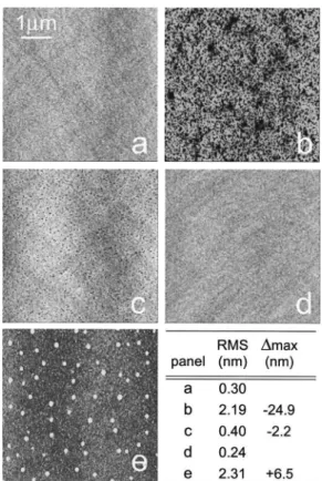
One of the objectives of the present study was the deter-mination of an optimum oxide removal method that would minimize surface roughness. Although reliance on a com-plete oxide removal by exposure to Ga flux at a lower tem-perature looks attractive, it carries the inherent risk of gen-erating Ga droplets on the surface. Indeed, the inhomogeneous nature of this process means that when 90% of the oxide is removed, the remaining 10% is most likely left in the form of patches. At this point most of the supplied Ga atoms will adsorb directly on the clean GaAs surface. Although some atoms will migrate and react with the re-maining oxide, a large fraction will start to form droplets. Figure 3 shows a series of AFM images illustrating the ef-fects of the combined approach proposed in the present study. The labeling of the panels follows the labels on the arrows used in the bottom panel of Fig. 1 to indicate sche-matically at which point the exposure to the Ga flux was terminated for the process corresponding to each individual AFM image. Figure 3~a! shows the typical morphology of an epi-ready GaAs surface without any further treatment. This surface has a rms roughness of 0.3 nm and most likely rep-resents state-of-the-art surface smoothness that can be ob-tained with chemomechanical polishing. Figure 3~b! shows the morphology of another quarter from the same substrate, which was subject to standard oxide desorption. Apart from the strong overall increase in the local roughness, one imme-diately notices a high density of surface pits, about 100 nm in diameter, some of them exceeding 20 nm in depth D ~rms 52.19 nm, D max5224.9 nm!. Such morphology is consis-tent with other literature reports.1–3,6 Figure 3~c! shows the morphology of a wafer where approximately 70% of the ox-ide was removed with Ga exposure, while the rest was evaporated during the following temperature ramp. Although some pitting is still present, the improvement in morphology compared to standard desorption is dramatic. The rms rough-ness decreased by a factor of 5, while the depth of the pits decreased by more than one order of magnitude ~rms50.4
nm, D max522.2 nm!. Figure 3~d! shows a typical wafer morphology after nearly 90% of the oxide had been removed during the pulsed Ga exposure stage. The pitting is elimi-nated completely, and the measured rms roughness of 0.24 nm is slightly smaller than that for the untreated epi-ready wafer, probably indicating some surface smoothing achieved during the annealing stage. The supply of only one additional Ga pulse to the surface during the low-temperature stage, which increases the fraction of removed oxide to 95% ~not shown in this figure!, results in the generation of Ga droplets that cannot be dissolved during the subsequent temperature ramp and anneal. Figure 3~e! shows the surface morphology for the case where the surface was exposed to a Ga flux approximately 15% larger than that needed for complete ox-ide removal. A large number of mounds is visible in former locations of Ga droplets. TEM measurements done on GaAs layers grown on such a substrate showed no evidence of metallic Ga precipitates at the substrate–epilayer interface, which indicates that the majority of Ga droplets were con-verted to GaAs during annealing under As flux. Nevertheless we found that such mounds were very hard to planarize
dur-FIG. 3. Representative morphologies of the GaAs surface after different oxide removal treatments measured by AFM. All panels are 535mm in size, and the gray scale has been optimized individually for each panel to reveal surface features. The table summarizing rms roughness and maximum depth D max ~or height! of localized features is included in the lower right corner. ~a! Epi-ready substrate as-received. ~b! The surface after standard thermal oxide desorption. ~c! The surface where 70% of the oxide was desorbed with atomic Ga exposure, while the remaining 30% was desorbed thermally. ~d! The surface where 90% of the oxide was desorbed with atomic Ga exposure, with the remaining 10% desorbed thermally. ~e! The substrate where 15% more Ga was delivered to the surface than needed for total oxide conversion.
ing subsequent epitaxy, making Ga droplet formation during oxide removal very undesirable.
When comparing the surface morphology of wafers pre-pared using the standard oxide desorption procedure we found little qualitative difference in the roughness and pitting for all substrates used, with the exception of a fresh ~three weeks old! epi-ready substrate, where the surface morphol-ogy after standard oxide desorption showed considerably smaller pit density. The latter nevertheless exhibited large rms roughness ~;1 nm!, and the depth of the individual sur-face pits was still large ~D max of 218.4 nm!. On the other hand, regardless of the age of the epi-ready preparation, sub-stantial improvement of the substrate morphology after the oxide desorption was obtained by employing the two-stage process, with the partial oxide removal by exposure to Ga flux at temperatures below 500 °C. The experiments per-formed on the oldest epi-ready wafers used in the present study, which were stored for four years in an opened cassette rather than a sealed nitrogen filled bag, showed a still con-siderable, albeit smaller benefit of the partial oxide removal with Ga exposure, indicating that the corrosion of the GaAs by Ga2O3 has already started during wafer storage,
consis-tent with reports by Allwood et al.5Nevertheless, a removal of about 80% of the oxide during the Ga exposure stage from these wafers resulted in the rms roughness of 0.57 nm and D max of 27.8 nm, which is by a factor of 2 better than for standard oxide desorption from the fresh epi-ready substrate. Another important question addressed in the present study was the amount of contamination left at the substrate– epilayer interface for different oxide removal procedures and a different age of the epi-ready substrates. For that purpose we have grown 200 nm thick GaAs layers, following the complete oxide desorption procedures described above on selected wafers from all the substrate batches studied, and measured the interface contamination by SIMS. We found that within a factor of 2 the interfacial oxygen, carbon, and silicon concentrations were the same for all the layers with no obvious trends, except for the very fresh wafer, where all the investigated contaminants were by about 20% lower than the next ‘‘cleanest’’ wafer. This might indicate that contrary to common belief most of the C, Si, and O contamination routinely found at the surface of epi-ready wafers is intro-duced during the initial surface preparation at the factory rather than during the subsequent storage and handling.
IV. CONCLUSIONS
We have proposed a modified procedure for the oxide removal from epi-ready GaAs ~001! substrates that consists
of the standard thermal oxide removal procedure preceded by partial oxide removal at lower temperatures via the con-version of the stable Ga2O3 oxide to a volatile Ga2O oxide
by a pulsed supply of Ga atoms in the absence of an As flux. For a wide selection of wafers provided by different suppli-ers and varying in age or storage conditions, we found that such an approach reduces the rms roughness and surface pit-ting by more than one order of magnitude even if only 70% of the initial oxide is removed in the low-temperature stage. The removal of about 90% of the oxide during the low-temperature stage generally results in nearly atomically flat pre-epi substrates. Although for our studies the Ga pulses were applied at constant temperature, the procedure can be implemented during the standard temperature ramp to 630 °C, as long as the Ga is delivered to the surface in the absence of an As flux in the approximate temperature range of 440 °C to 530 °C. Through the kinetic studies of RHEED pattern evolution we demonstrated that the oxide removal with exposure to Ga flux is laterally inhomogeneous. Conse-quently, the complete removal of the oxide using only this method, albeit always possible, would be very hard to achieve consistently without the generation of Ga droplets on the GaAs surface.
SIMS studies performed on epitaxial layers indicate that even though the standard oxide desorption procedure re-moves a considerable amount of top GaAs substrate along with the oxide, it leaves behind as much surface contamina-tion as the more gentle and controlled process examined in the present work. Clearly, for the structures where impurity accumulation at the substrate interface cannot be tolerated, additional measures such as a combination of HF dip and
in-situ atomic hydrogen cleaning1would have to be taken.
1M. Adamcyk, A. Ballestad, T. Pinnington, T. Tiedje, M. Davies, and Y.
Feng, J. Vac. Sci. Technol. B 18, 1488 ~2000!.
2A. Ballestad, B. J. Ruck, M. Adamcyk, T. Pinnington, and T. Tiedje, Phys.
Rev. Lett. 86, 2377 ~2001!.
3
A. Ballestad, B. J. Ruck, J. H. Schmid, M. Adamcyk, E. Nodwell, C. Nicoll, and T. Tiedje, Phys. Rev. B 65, 205302 ~2002!.
4D. Allwood, N. Mason, A. Mowbray, and R. Palmer, J. Cryst. Growth 248, 108 ~2003!.
5
D. A. Allwood, S. Cox, N. J. Mason, R. Palmer, R. Young, and P. J. Walker, Thin Solid Films 412, 76 ~2002!.
6Y. Asaoka, J. Cryst. Growth 251, 40 ~2003!.