The MIT Faculty has made this article openly available.
Please share
how this access benefits you. Your story matters.
Citation
Shen, Bin et al., "Broadband couplers for hybrid
silicon-chalcogenide glass photonic integrated circuits." Optics Express 27,
10 (May 2019): 13781-92 doi. 10.1364/OE.27.013781 ©2019 Authors
As Published
https://dx.doi.org/10.1364/OE.27.013781
Publisher
The Optical Society
Version
Final published version
Citable link
https://hdl.handle.net/1721.1/128530
Terms of Use
Article is made available in accordance with the publisher's
policy and may be subject to US copyright law. Please refer to the
publisher's site for terms of use.
Broadband couplers for hybrid
silicon-chalcogenide glass photonic integrated
circuits
BIN SHEN,
1HONGTAO LIN,
2FLORIAN MERGET,
1SAEED SHARIF AZADEH,
1CHAO LI,
3,6GUO-QIANG LO,
3,6KATHLEEN A. RICHARDSON,
4JUEJUN HU,
5AND JEREMY WITZENS1,*
1Institute of Integrated Photonics, RWTH Aachen University, Sommerfeldstr. 18/24, 52074 Aachen,
Germany
2College of Information Science & Electronic Engineering, Zhejiang University, Hangzhou, China 3Institute of Microelectronics (IME)/A*STAR, Science Park Road 11, Singapore
4College of Optics and Photonics, University of Central Florida, 4304 Scorpius St., Orlando, FL
32816-2700, USA
5Department of Materials Science & Engineering, Massachusetts Institute of Technology, Cambridge,
MA 02139, USA
6Currently with Advanced Micro Foundry Pte Ltd. (AMF), Singapore
*jwitzens@iph.rwth-aachen.de
Abstract: We report on the design, fabrication and testing of three types of coupling
structures for hybrid chalcogenide glass Ge23Sb7S70-Silicon (GeSbS-Si) photonic integrated
circuit platforms. The first type is a fully etched GeSbS grating coupler defined directly in the GeSbS film. Coupling losses of 5.3 dB and waveguide-to-waveguide back-reflections of 3.4% were measured at a wavelength of 1553 nm. Hybrid GeSbS-to-Si butt couplers and adiabatic couplers transmitting light between GeSbS and Si single-mode waveguides were further developed. The hybrid butt couplers (HBCs) feature coupling losses of 2.7 dB and 9.2% back-reflection. The hybrid adiabatic couplers (HACs) exhibit coupling losses of 0.7 dB and negligible back-reflection. Both HBCs and HACs have passbands exceeding the 100 nm measurement range of the test setup. GeSbS grating couplers and GeSbS-to-Si waveguide couplers can be co-fabricated in the same process flow, providing, for example, a means to first couple high optical power levels required for nonlinear signal processing directly into GeSbS waveguides and to later transition into Si waveguides after attenuation of the pump. Moreover, GeSbS waveguides and HBC transitions have been fabricated on post-processed silicon photonics chips obtained from a commercially available foundry service, with a previously deposited 2 μm thick top waveguide cladding. This fabrication protocol demonstrates the compatibility of the developed integration scheme with standard silicon photonics technology with a complete back-end-of-line process.
© 2019 Optical Society of America under the terms of the OSA Open Access Publishing Agreement
1. Introduction
Silicon photonics (SiP) in the silicon-on-insulator (SOI) platform has attracted great interest in research and industry in the past decades [1]. Compatibility with the complementary metal oxide semiconductor (CMOS) technology has allowed for low-cost manufacturing and commercialization of SiP devices. Utilization of the free-carrier plasma dispersion effect, as well as integration with other selectively grown or heterogeneously integrated semiconductor materials has enabled a wide range of functionalities encompassing electro-optic modulation [2], photodetection [3] and light generation [4].
Si has a large refractive index and is transparent in the near infrared C- and O- communication bands. It also has a high optical damage threshold and high third order
#360673 https://doi.org/10.1364/OE.27.013781
nonlinearity, which are very important features for all optical signal processing and wavelength conversion [5]. However, these applications are limited by the large two-photon absorption (TPA) of Si [6]. One way to overcome this problem is to integrate chalcogenide glasses into the SOI platform. Chalcogenide glasses, which contain one or more of the chalcogen elements including S, Se and Te and are covalently formed with network formers such as Ge, Sb or As, have large third order nonlinearities and a much smaller TPA coefficient than that of Si [7]. Thanks to their remarkable optical properties such as large and tailorable refractive index, low loss, broad transparency region, and high optical nonlinearity, chalcogenide glasses have been demonstrated to be promising materials for a broad range of applications such as sensors [8,9], unconventional substrate integration [10,11], and all-optical signal processing [12]. Rekindled interest in nonlinear-based transmission by means of the nonlinear Fourier transform [13] may also increase interest in manipulation of solitons with highly nonlinear fibers [14,15] or on-chip waveguides [16]. In another optical communications application, phase sensitive amplification based on parametric amplification and its on-chip implementation has recently gained great interest [17]. Hybrid integration of As2S3 devices on silicon has enabled stimulated Brillouin scattering (SBS) [18], which allows
bringing a number of applications such as SBS enabled tunable time delays [19] and SBS enabled ultrahigh-resolution spectroscopy [20] on chip [21].
While previous works have investigated hybrid waveguides composed of both chalcogenides and Si, for example by infiltration of a Si slot waveguide, thus also obtaining enhancement of the optical intensity inside the chalcogenide [22], here we completely transition between Si and GeSbS waveguides in order not to be penalized by Si TPA inside the GeSbS waveguides. One of the main issues of integrating chalcogenide glasses into the SOI platform in this way is to couple light to and from the chalcogenide devices. Here, we focus on the efficient coupling of light into GeSbS chalcogenide glass waveguides hybridly integrated into the SOI platform by post-processing of chips fabricated in a standard SiP foundry, Singapore’s Institute of Microelectronics (IME). Another issue is to define a fabrication flow and device geometries that allow for post-processing of fully fabricated SiP chips with a fully fabricated back-end-of-line (BEOL) stack. Indeed, it is our objective to integrate GeSbS based devices in a fully functional standard SiP platform with electro-optic functionality. This prevents, for example, relying on additional etch-stop layers other than those already present in the process.
At a wavelength of 1550 nm, GeSbS has a refractive index of 2.17, a third order nonlinear index on the order of
1 0 m / W
−18 2 , and negligible TPA [23,24]. It is important to note that reported values for these properties can vary widely depending on material form (bulk or planar film), measurement wavelength and specific characterization method. The linear loss of single-mode GeSbS waveguides can be as low as 0.5 dB/cm [25,26]. Compared to arsenic-based chalcogenide glasses, GeSbS has low toxicity.In this paper, three types of coupling structures have been designed, fabricated and analyzed. First, we present the design and experimental validation of a fully etched GeSbS grating coupler (GC) allowing direct coupling of light into GeSbS waveguides (Section 2), which can be advantageous for the first signal processing stage, e.g. if optical power initially exceeds levels that can be transported in Si waveguides without incurring high TPA induced losses. Next, we demonstrate two couplers between GeSbS and silicon nanowire waveguides, a GeSbS-Si hybrid butt coupler (HBC), Section 3, and a GeSbS-Si hybrid adiabatic coupler (HAC), Section 4. These approaches are benchmarked against each other in terms of insertion losses and back-reflections.
In all three cases, GeSbS waveguides are fabricated out of a 500 nm thick film deposited on top of SiP chips after post-processing, enabling their co-fabrication in a common hybrid technology platform. Coupling structures provide connectivity to 900 nm wide, fully etched GeSbS waveguides, either directly from a standard single-mode optical fiber with a 10.4 μm mode field diameter (MFD) in the case of the GC, or to and from fully etched, 400 nm by 220
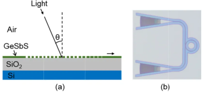
nm Si wavegu anomalous di light generati structures, Ge possible in or µm in the GC GeSbS bus w monitor wave of the SOI w Bending radii losses – as v experimental 2. GeSbS gr We first inve waveguides. T GeSbS GCs directly inject light first tran Si hybrid cou devices after n 2.1. GeSbS The focusing angle θ of 11 chalcogenide using single-s ion etching w waveguides a to let the beam GC pair, conn be found in [2 Fig. 1 fabric A grating analytical calc fiber mode w apodization st located 34.9 μ
uides. The GeS ispersion at 15 ion, an impor eSbS waveguid der to minimiz C, HBC and H waveguide is in eguide losses. A wafer’s buried i of 20 μm us verified by sim data. rating couple estigate fully e The fabrication and GeSbS w ted into the G nsits through Si uplers described nonlinear proc grating coupl GC [27] is d degrees [Fig. layer is depos source thermal with CHF3/CF
are fully etched m freely diffra nected by a wa 25].
1. (a) Schematic cated GC pair, wav period of 13 culations [28]. with an MFD tarts with a tre μm from the en SbS waveguide 50 nm. The la rtant target ap de lengths (inc ze waveguide l HAC test struct ncluded in eac All the GeSbS oxide (BOX), sed in the GeS mulations – and er etched GeSbS n process is fa waveguides in GeSbS material i waveguides ( d in the follow essing. ler design and designed for co 1(a)] and a tran sited on top of
evaporation. A
4 (3:1), the to
d. The full angl ct. Figure 1(b) aveguide loop c
diagram of the veguide and ring re 41 nm with a . In order to fu D of 10.4 µm ench width of 1 nd of the wave e geometry ens atter allows eff pplication of cluding tapered osses and are r tures. A GeSb ch of the test
waveguides ar or, in the cas SbS waveguide d do not skew GCs for coup acilitated by th a single litho l, allowing a l as a consequen wing sections al d fabrication oupling into a nsverse electric f an oxidized S After electron op of the GC le of the GC ta ) shows an opti coupled to a RR GeSbS GC. (b) esonator. a trench width urther improve m, the first 16 135 nm and a p eguide, and end
sures single-mo ficient phase m chalcogenide d sections) are respectively 24 S ring resonat structures in are air clad and se of the GCs, e routing resul w the insertion pling of light he joint fabrica graphy and et arger input op nce of the latte llow transfer o
fiber mode w c (TE) polariza Si wafer with a beam lithograp
is left air cla aper is 21 degr ical microscop R. The specific Optical microsco h of 762 nm w e the coupling 6 grooves wer period of 1007 ds with the ful
ode operation a matching for p materials. In e maintained as 44 µm, 223 µm tor (RR) coupl order to indep d located direct , an oxidized lts in negligib n losses extrac to GeSbS sin ation of the ful tch step. Here ptical power th er’s large TPA) of light into the
with a forward ation. The 500 a 3 μm thick S phy (EBL) and ad. Grooves as rees, which is pe image of a f c fabrication d
ope image of the was first obtai efficiency to a re apodized [ 7 nm for the fir
ll 762 nm trenc as well as arametric nside test s short as m and 223 led to the pendently tly on top Si wafer. ble excess cted from gle-mode lly etched e, light is han if the ). GeSbS-e Si basGeSbS-ed coupling nm thick SiO2 layer d reactive s well as sufficient fabricated details can e ined with an optical [29]. The rst trench ch / 1341
nm period at time-domain Grating coup waveguide w (2D) FDTD s 2.2. GeSbS Figure 2(a) sh of 0 dBm. Th nm. The mini resulting from 2(b)], we dete waveguide lo be distinguish losses feature range. Excess might be over the loss per G GeSbS GC lo shallow-etche comparing to fabrication ste Fig. 2 smoot curve close As shown 39 nm and 80 bandwidth is spectrum con the input and resonance [32 elsewhere in t by applying resonances. the 17th tren (FDTD) simu pler insertion ere simulated imulation. grating coupl hows the transm he radius of th
imum insertion m two GCs and ermine the intr ss of 4.0 dB/c hed from each e the expected s coupler losse restimated. Th GC is extracte oss of 7.5 dB ed GeSbS GC o the shallow-eps, making th 2. (a) Transmissio thed transmission . (b) Measuremen to 1550 nm and its n in Fig. 2(a), t 0 nm, respectiv limited by the ntains a 0.6 dB output GCs as 2], we calculat this paper smo a 1st order S nch. Apodizatio lations perform losses betwe to be 4.9 dB ler insertion lo mission spectru he RR is 100 µ n loss of 10.6 d d the 244 µm lo rinsic quality f cm, wherein co other based on increase with es were not de
e loss from the d to be 5.3 dB reported by S Cs reported by -etched GCs, eir fabrication n spectrum of the spectrum of the G nt data (blue dots)
s Lorentzian fit (re the 1 dB and 3 vely. For a sing e wavelength B Fabry-Perot r corroborated b te that 3.4% o oothed transmi Savitzky-Golay on was iterativ med with the een single mo at a waveleng osses um of the fabri µm, resulting in dB is achieved ong waveguide factor of the R oupling losses n their wavelen h wavelength, eembedded so e short GeSbS B. This couple Serna et al. [30 y Chiles et al. the fully etch much easier.
e GeSbS device w GC loop, with ripp ) in a smaller wav ed line). 3 dB bandwidth gle GC, the 1 d range of the e ripple, which i by the FSR of f the light is b ssion spectra [ y smoothing vely optimized commercial si ode fiber and gth of 1550 nm icated GeSbS G n a free spectr d at 1553 nm, w e. By fitting th RR to be 110,0 and intrinsic w ngth dependen the intrinsic lo o that the extra S waveguide is er loss is bette 0], and is sligh ., 4.3 dB ± 0 hed GCs descr
with an input pow ples filtered out, i velength range ar ths of the GC p dB bandwidth equipment. It is due to the b 2.0 nm. By an back-reflected [red curve in F filter after m d with finite-d imulation tool d single mode m in a two-dim GC with an inp ral range (FSR which include he resonance cu 000, correspon waveguide los nce. While the
osses remain i acted wavegui thus negligibl er than the ful htly worse tha 0.7 dB [31]. H
ribed here ne
wer of 0 dBm. The is shown by a red round a resonance pair are measu is 60 nm, and is notable that back-reflection nalyzing the Fab
by each GC. Fig. 2(a)] were manually remo difference RSOFT. e GeSbS mensional put power R) of 1.54 s the loss urve [Fig. nding to a ses could coupling in a tight ide losses le, so that ly etched an that of However, eed fewer e d e ured to be the 3 dB t the loss n between bry-Perot Here and obtained oving the
3. GeSbS-Si hybrid butt coupler
GeSbS-Si hybrid couplers are required to transmit light between GeSbS and Si single-mode waveguides. One intuitive hybrid coupler structure is the GeSbS-Si HBC, in which forward tapered GeSbS waveguides are butt-coupled to inverse tapered Si waveguides. This is similar to inverse couplers used for fiber-to-chip edge coupling [33] but further adapted to enable local BEOL removal. The goal here is to apply them to fully processed SiP chips.
3.1. GeSbS-Si hybrid butt coupler design and fabrication
In the HBC loop, light is coupled in and out of the chip through silicon GCs. The silicon GCs are followed by SiO2 clad silicon waveguides with a thickness of 220 nm and a width of 400
nm, which are connected to a 500 nm thick GeSbS waveguide via the HBCs [Fig. 3(a)]. Figures 3(b) and 3(c) show a zoomed-in microscope image as well as a schematic of the HBC. To achieve maximum coupling efficiency, the coupling structure is designed so that the center of the Si waveguide mode lines up with the center of the GeSbS waveguide mode in both the vertical and horizontal directions. Therefore, the BEOL layer stack as well as 90 nm of the BOX layer are removed in the area of the GeSbS waveguide. To ensure a precise etch stop during BEOL removal, a partially etched Si device layer (deep-etched Si with a remaining slab height of 90 nm) is used as an etch stop. This Si layer is then removed during the same etch sequence by switching the etching chemistry. Finally, the top 90 nm of the BOX layer is removed by a third dry etch.
To avoid scattering at the onset of the etch stop layer, the silicon waveguide is adiabatically transformed from a fully etched ridge into a deep-etched rib waveguide. Over a length of 15 µm, the silicon waveguide slab is tapered up to a total width of 3 µm. At the same time, the silicon waveguide core is tapered down from 400 nm to 200 nm in order to expand the mode and match its dimensions to the GeSbS waveguide. The waveguide core (but not the 90 nm etch stop layer) is terminated 1 µm before the nominal GeSbS taper facet position to accommodate lithographic overlay tolerances. As a result of this process, a residual nominally 1 µm wide layer of deep-etched silicon remains between the end of the silicon rib waveguide and the facet of the GeSbS taper. A 40 µm long GeSbS taper adiabatically narrows the GeSbS waveguide from a parameterized initial width (see below) to the 900 nm standard single-mode waveguide width used in this work.
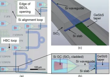
As shown in Fig. 3(a), all-silicon alignment loops (SAL) with SiO2 cladding are fabricated
on the chip besides the HBC loops. The SALs have the same silicon GCs as the HBC loops, which are connected with a 140 µm long silicon waveguide resulting in negligible additional losses. They are used as reference structures to obtain the silicon GC losses needed to deconvolve the HBC losses.
The silicon GCs and waveguides were fabricated within the IME SiP platform with 248 nm deep UV lithography [34]. The GeSbS HBC devices were fabricated by EBL and RIE during post-processing of the chips, with fabrication details in [25].
Fig. 3. (a) Optical microscope image of HBC loops and a Si reference loop. (b) Optical microscope image of a Si GC (SiO2 clad) and a GeSbS-Si HBC. (c) Schematic view of a GeSbS-Si HBC.
3.2. GeSbS-Si hybrid butt coupling loss
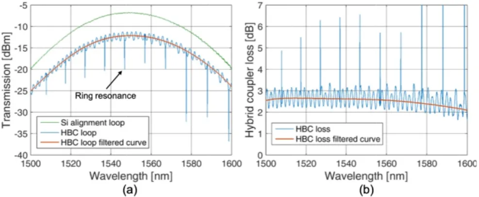
Figure 4(a) shows the transmission spectra of an SAL and an HBC loop, both with an input power of 0 dBm. This HBC loop has a GeSbS taper width of 2.5 µm. The GeSbS waveguide loop is coupled to a RR with a radius of 15 µm, which results in an FSR of 9.9 nm. Since the minimum insertion loss of both loops is obtained at 1552 nm, we use it as the reference wavelength for the loss comparison (since it is also the wavelength at which data analysis is the most robust against GC peak wavelength variations). The total insertion losses of the SAL and HBC loops are respectively 6.8 dB and 12.2 dB at 1552 nm.
By fitting the resonance of the GeSbS RR, we extract losses of 5.5 dB/cm. Therefore, the optical loss resulting from the 223 µm long GeSbS waveguide loop is also negligible. Thus, by subtracting the insertion loss of the SAL from the insertion loss of the HBC loop, we get the HBC loss
( ) - ( )
=
2
Insertion Loss HBC Loop Insertion Loss SAL
Hybrid Coupler Loss (1)
Figure 4(b) shows the loss spectrum of the HBC, with 2.7 dB losses at 1552 nm. The 1 dB and 3 dB optical bandwidths of the SAL and HBC loops are both 28 nm and 49 nm, respectively. Thus, the optical bandwidth of the HBC loop is determined by the silicon GCs. We can see in Fig. 4(b) that the 1 dB bandwidth of a single HBC is larger than 100 nm, which is the measurement range limit of our equipment.
The loss spectrum of the HBC contains 1.6 dB Fabry-Perot ripples, which is attributed to the back-reflection between the GeSbS-Si coupling facets as also corroborated by an FSR of 2.1 nm correlating with the 223 μm GeSbS waveguide length [note that Fig. 4(b) shows half the ripple strength since the transfer function of the loop, in dB, has been halved to normalize the losses to a single GC]. By analyzing the Fabry-Perot resonances [32], we evaluate the HBC reflection to be 9.2%.
A series of HBC loops with varying taper width have been fabricated to characterize its influence on the HBC loss. Figure 5 shows the simulated and measured HBC losses at 1552 nm as a function of the GeSbS taper width. In the measured data, the HBC has a minimum loss of 2.7 dB with a GeSbS taper width of 2.5 µm. Overall, good agreement is found between simulated and measured HBC losses; in particular, dependency on GeSbS taper width is predicted well.
Fig. 4 power out, is filtere Fig. 5 functi ripple 4. GeSbS-S In order to mi designed and SiP edge cou waveguide em such as polym light between coupling loss thicknesses co show the po performance w easier to fabr performance w 4.1. GeSbS-In the HAC lo standard 400 nm (compatib the silicon GC (PIC) was tak
4. (a) Transmission r of 0 dBm. The s s shown by a red c ed version (red line
5. Simulated (red l ion of GeSbS tape es. The blue curve
i hybrid adia inimize hybrid fabricated HA uplers consist mbedded in a la mers or SiON n single-mode [18]. Here, w ompatible with ossibility of c with the previ ricate in standa
will help to tra -Si hybrid adia
oops, light is c nm (width) by ble with the 24 Cs and the silic ken from the f
n spectra of SAL smoothed transmis curve. (b) Raw HB e).
ine), measured (bl er width. The error is a polynomial fit
abatic couple
d coupling loss AC type coupl ting in mode arger core wav
[35]. Morrison Si waveguide e adapt these c h prior grating co-fabricating ously describe ard SiP chips b ade-off fabricat abatic couple coupled in and y 220 nm (heig 48 nm DUV lit con waveguide fabrication fac
(green line) and H ssion spectrum of
BC loss spectrum
lue dots) and inter r bars correspond t t to help guiding th
er
as well as bac ers. These hav
size converte veguide made o n et al. have d s and As2S3 w couplers to the g coupling of t them with G ed HBCs. Sinc by means of B tion complexity r design and out of the chip ght) waveguide hography) ove es are air clad, cility before ba
HBC loops (blue l the HBC loop, w featuring ripples
rpolated (blue line to the magnitude o he eye. ck-reflections a ve a similar pr ers with an i out of lower re demonstrated A waveguides for e Si-GeSbS ma the light. This GCs, as well ce, as describe BEOL deproce y with perform fabrication p through silico es are tapered d er a taper lengt
as the SiP pho ack-end fabrica
line) with an input with ripples filtered (blue line) and its
e) HBC losses as a of the Fabry-Perot at the interface, rinciple of ope inverse tapere fractive index As2S3 HAC to r SBS with lo aterial system allows in par as to comp d below, the H essing, a comp mance. on GCs [Fig. 6 down to a wid th of 15 µm. H otonic integrat ation. Figures t d s a t , we have eration as d silicon materials o transmit ow hybrid with film rticular to pare their HBCs are parison of 6(a)]. The dth of 200 Here, both ed circuit 6(b) and
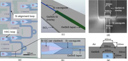
6(c) show a magnified microscope image as well as a schematic view of an HAC. A 500 nm GeSbS film is deposited on top of the chip and subsequently etched to form GeSbS waveguides. A GeSbS waveguide with a parameterized initial width overlays the entire Si taper. After termination of the Si taper, the GeSbS waveguide is tapered down to the standard 900 nm width over a length of 40 µm. Figure 6(d) shows a scanning electron microscope (SEM) image of the GeSbS-Si overlay. It can be seen that the GeSbS film forms a bump where it overlays the Si waveguide. The cross section of the GeSbS bump is close to an isosceles trapezoid with upper and lower widths of respectively 400 nm and 608 nm. Since the SEM image was taken at an angle, the height of the bump cannot be directly extracted from the micrograph. However, based on rescaling of the known 500 nm height of the GeSbS film, the height of the bump was verified to be approximately 220 nm, coinciding as expected with the Si waveguide height. Figure 6(e) shows the cross section of the coupler at the point where the overlay starts, as assumed in the 3D-FDTD simulation. As the Si waveguide is tapered down along the main axis of the coupler, the GeSbS bump is also tapered down by the same amount, with a constant offset maintained between the waveguide width and the lower width of the isosceles trapezoid. The differences between the simulated HAC coupler losses with and without the GeSbS bump are negligible.
As shown in Fig. 6(a), a pure silicon alignment loop with air cladding (SALair) is
fabricated on the chip besides the HAC loops. The SALair comprises the same Si GC as in the
previous section, as well as a 140 µm long silicon waveguide. However, insertion losses and peak wavelength are changed due to the top air cladding.
Here too, the Si PICs were fabricated within the IME SiP platform with 248 nm deep UV lithography [34] and subsequently post-processed with EBL after GeSbS film deposition.
Fig. 6. (a) Optical microscope image of HAC loops and a Si reference loop. (b) Optical microscope image of a Si GC (air clad) and a Si HAC. (c) Schematic view of a GeSbS-Si HAC. (d) SEM image of the front facet of the GeSbS-GeSbS-Si overlay. (e) Cross-section of the starting point of the GeSbS-Si overlay in the FDTD simulations.
4.2. GeSbS-Si hybrid adiabatic coupling loss
Figure 7(a) shows the transmission spectra of a SALair and a HAC loop with an input power
of 0 dBm. This HAC loop has an initial GeSbS taper width of 1.5 µm. As for the HBC loops, the GeSbS waveguide of the HAC loops is coupled to a 15 µm RR with an FSR of 9.9 nm. The minimum loss of the SALair is obtained at 1523 nm, at which the insertion losses of the
SALair and of the HAC loop are respectively 9.1 dB and 10.5 dB. By fitting the resonance of
the GeSbS RR, we extract losses of 5.6 dB/cm. Similarly to the HBC chip, the waveguide losses inside the SALair and HAC loop are negligible. The HAC loss is half of the insertion
losses of the H 0.7 dB inserti The 1 dB respectively. and 57 nm, re wavelength ra HAC. As for the measurem Fig. 7 input red cu The loss (small ripples which means loop. Fig. 8 as a fu measu width guidin A series o characterize i losses at 1523 width of 0.5 µ narrower rang
HAC loop afte on loss. B bandwidth o The 3 dB band espectively, wi ange of the eq the HBC, the ment range limit
7. (a) Transmissio power of 0 dBm. urve. (b) HAC loss
spectrum of th s due to the Si
that the HAC
8. (a) Simulated (r unction of GeSbS ured losses. Optica s of 0.5 µm (b) an ng the eye. of HAC loops ts influence on 3 nm as a func µm is 10.6 dB ge. The minim
er subtraction o of the SALair
dwidth of the ith the measure quipment. Figu deembedded 1 t of our equipm
n spectra of an SA The smoothed tra s spectrum (blue li he HAC loop
GCs are prese loop does not
red line), measured taper width. The e al microscope ima nd 1.5 µm (c). As with variation n HAC loss. F ction of the Ge
, and was omit mum measured
of the SALair lo
and of the H SALair and of
ed 3 dB bandw ure 7(b) show 1 dB bandwidt ment.
ALair (green line) ansmission spectru ne) and its smooth
does not cont ent in the raw s induce obviou
d (blue dots) and error bars correspo ages of the GeSbS s in Fig. 5, the blu ns of the initial igure 8(a) show eSbS taper wid
tted from the f HAC loss is 0
osses. At 1523 HAC loop ar the HAC loop width of the HA ws the extracte
th of the HAC
and HAC loop (b um of the HAC lo hed equivalent (red tain any obvio spectra of both us back-reflect
interpolated (blue ond to the standard S-Si HACs with in ue curve is a poly l taper width h ws the simulat dth. The HAC figure in order 0.7 dB at a Ge 3 nm, the HAC re 37 nm and p are larger tha
AC loop limite d loss spectru C is larger than
blue line) with an oop is shown as a d line).
ous Fabry-Pero h loops and can tion as seen in
e line) HAC losses d deviations of the nitial GeSbS taper ynomial fit to help have been fabr ted and measu C loss with GeS
r to keep the y eSbS taper wid
C features d 38 nm, an 54 nm ed by the um of the n 100 nm, n a ot ripples ncel out), the HBC s e r p ricated to ured HAC SbS taper -axis in a dth of 1.5
µm. Good agreement is observed between simulated and measured losses for taper widths larger than 1.2 µm. However, for smaller GeSbS taper widths, measured losses become significantly larger than simulated losses. After visual inspection of the chips in an optical microscope, it appears this is caused by the GeSbS waveguide having defects in the region overlaying the Si waveguide for small GeSbS taper widths; such defects were not found for the wider tapers. Figures 8(b) and 8(c) show microscope images of GeSbS-Si HACs with GeSbS taper widths of 0.5 µm and 1.5 µm, respectively. We can see that in the GeSbS-Si overlay region, the HAC with 0.5 µm taper width is missing a piece of GeSbS waveguide, while the HAC with the 1.5 µm taper is free of defects.
Since the HAC couplers appear the superior devices in terms of back-reflection and insertion losses, it would be desirable to also implement them with a device configuration and a process flow compatible with fully fabricated SiP chips including a full BEOL process, as available from commercial foundry platforms. This would, however, be considerably harder for the HACs than for the previously described HBCs. While one could also envision replacing the fully etched ridge waveguides used in the HACs by partially etched rib waveguides in order to provide an etch stop at the bottom of the BEOL stack, this would only partially resolve the problem due to the resulting topology of the etch stop layer (since for the HACs the Si waveguide has to extend into the region where the BEOL is deprocessed). Wet SiO2 etches can be highly selective to a Si etch stop layer, however they cause their own set
of difficulties, such as undercutting of the protected areas. Dry etches typically used to etch SiO2 based on CHF3 or fluorocarbons (CxFy), while providing some selectivity [36], also
attack Si, so that the Si waveguiding layer appears likely to be damaged in such a process in the absence of other non-standard etch stop layers not available in standard SiP chips. The Si etch stop layer used for HBC fabrication on the other hand does not serve for waveguiding, is planar, and is completely removed as part of subsequent etches. Consequently, etch selectivity is much less of an issue there and the optical quality of resulting structures thus not as severally impacted.
The overall resilience of the utilized GeSbS material across the range of process conditions applied in this paper is also noteworthy, in particular its ability to maintain its optical properties and to remain relatively free of defects. This is all the more remarkable since other chalcogenide materials such as As2S3 or As2Se3 have historically suffered from
large variability in their post-deposition properties as well as increased defectivity.
5. Conclusions
Three types of coupling structures to GeSbS waveguides compatible with hybrid integration in a silicon photonics platform have been shown. The fully etched GeSbS grating coupler has a loss of 5.3 dB and results in 3.4% of the light being back-reflected into the GeSbS waveguide when it is coming from the latter. This grating coupler also allows injecting light directly into GeSbS, without a first Si based waveguide segment limiting the power, when nonlinear processing is targeted in a first device stage. Two alternatives, hybrid butt couplers and hybrid adiabatic couplers have been applied to transition between GeSbS and Si single-mode waveguides. The HBC has a 2.7 dB loss and 9.2% of the light is back reflected when injected from the GeSbS waveguide. The HAC has a reduced loss of 0.7 dB and negligible back-reflection.
While the HAC has better performance, both in terms of insertion losses and back-reflection, we were able to fabricate the HBCs on standard chips on which the back-end-of-line stack had been locally deprocessed. The HACs on the other hand were fabricated on chips from a wafer without back-end-of-line stack. In view of combining chalcogenide waveguides with a fully functional silicon photonics platform, the ability to easily deprocess the back-end-of-line is a big advantage. All devices have been designed and fabricated with the same GeSbS film thickness, so that the GeSbS-to-Si waveguide transitions can be co-fabricated with the grating couplers. For example, initial light injection into GeSbS
waveguides via grating couplers can be combined with a downstream transition into Si waveguides. Compatibility of waveguide transition geometries with back-end-of-line deprocessing is expected to be instrumental to combine GeSbS waveguides with the entire set of functionalities already available in standard silicon photonics platforms.
Funding
Deutsche Forschungsgemeinschaft (DFG) (403153975).
References
1. R. Soref, “The past, present, and future of silicon photonics,” J. Sel. Top. Quant. Electron. 12(6), 1678–1687 (2006).
2. J. Witzens, “High-speed silicon photonics modulators,” Proc. IEEE 106(12), 2158–2182 (2018).
3. L. Vivien, J. Osmond, J.-M. Fédéli, D. Marris-Morini, P. Crozat, J.-F. Damlencourt, E. Cassan, Y. Lecunff, and S. Laval, “42 GHz p.i.n Germanium photodetector integrated in a silicon-on-insulator waveguide,” Opt. Express
17(8), 6252–6257 (2009).
4. G. H. Duan, C. Jany, A. Le Liepve, A. Accard, M. Lamponi, D. Make, P. Kaspar, G. Levaufre, N. Girard, F. Lelarge, J.-M. Fedeli, A. Descos, B. Ben Bakir, S. Messaoudene, D. Bordel, S. Menezo, G. de Valicourt, S. Keyvaninia, G. Roelkens, D. Van Thourhout, D. J. Thompson, F. Y. Gardes, and G. T. Reed, “Hybrid III-V on silicon lasers for photonic integrated circuits on silicon,” J. Sel. Top. Quant. Electron. 20(4), 6100213 (2014). 5. B. Jalali and S. Fathpour, “Silicon photonics,” J. Lightwave Technol. 24(12), 4600–4615 (2006).
6. G. Priem, P. Bienstman, G. Morthier, and R. Baets, “Impact of absorption mechanisms on Kerr-nonlinear resonator behavior,” J. Appl. Phys. 99(6), 63103 (2006).
7. B. J. Eggleton, B. Luther-Davies, and K. Richardson, “Chalcogenide photonics,” Nat. Photonics 5(3), 141–148 (2011).
8. M.-L. Anne, J. Keirsse, V. Nazabal, K. Hyodo, S. Inoue, C. Boussard-Pledel, H. Lhermite, J. Charrier, K. Yanakata, O. Loreal, J. Le Person, F. Colas, C. Compère, and B. Bureau, “Chalcogenide glass optical waveguides for infrared biosensing,” Sensors (Basel) 9(9), 7398–7411 (2009).
9. D. M. Kita, H. Lin, A. Agarwal, K. Richardson, I. Luzinov, T. Gu, and J. Hu, “On-chip infrared spectroscopic sensing: redefining the benefits of scaling,” J. Sel. Top. Quant. Electron. 23(2), 340–349 (2017).
10. L. Li, H. Lin, S. Qiao, Y. Zou, S. Danto, K. Richardson, J. D. Musgraves, N. Lu, and J. Hu, “Integrated flexible chalcogenide glass photonic devices,” Nat. Photonics 8(8), 643–649 (2014).
11. H. Lin, Y. Song, Y. Huang, D. Kita, S. Deckoff-Jones, K. Wang, L. Li, J. Li, H. Zheng, Z. Luo, H. Wang, S. Novak, A. Yadav, C.-C. Huang, R.-J. Shiue, D. Englund, T. Gu, D. Hewak, K. Richardson, J. Kong, and J. Hu, “Chalcogenide glass-on-graphene photonics,” Nat. Photonics 11(12), 798–805 (2017).
12. V. G. Ta’eed, M. Shokooh-Saremi, L. Fu, D. J. Moss, M. Rochette, I. C. M. Littler, B. J. Eggleton, Y. Ruan, and B. Luther-Davies, “Integrated all-optical pulse regenerator in chalcogenide waveguides,” Opt. Lett. 30(21), 2900–2902 (2005).
13. S. K. Turitsyn, J. E. Prilepsky, S. T. Le, S. Wahls, L. L. Frumin, M. Kamalian, and S. A. Derevyanko, “Nonlinear Fourier transform for optical data processing and transmission: advances and perspectives,” Optica
4(3), 307–322 (2017).
14. L. Melnikov, “Soliton fission and fusion in dispersion oscillating fiber and correlation properties of the pulses,” in International Conference Laser Optics (IEEE, 2016) pp. R8–7.
15. S. Li, J. Koch, and S. Pachnicke, “Optical signal processing in the discrete nonlinear frequency domain,” in
Optical Fiber Communication Conference (Optical Society of America, 2018), paper W2A.40.
16. X. Gai, S. Madden, D.-Y. Choi, D. Bulla, and B. Luther-Davies, “Dispersion engineered Ge11.5As24Se64.5 nanowires with a nonlinear parameter of 136 W−1m−1 at 1550 nm,” Opt. Express 18(18), 18866–18874 (2010). 17. E. Liebig, I. Sackey, T. Richter, A. Gajda, A. Peczek, L. Zimmermann, K. Petermann, and C. Schubert,
“Performance evaluation of a silicon waveguide for phase regeneration of a QPSK signal,” J. Lightwave Technol. 35(6), 1149–1156 (2017).
18. B. Morrison, A. Casas-Bedoya, G. Ren, K. Vu, Y. Liu, A. Zarifi, T. G. Nguyen, D.-Y. Choi, D. Marpaung, S. J. Madden, A. Mitchell, and B. J. Eggleton, “Compact Brillouin devices through hybrid integration on silicon,” Optica 4(8), 847–854 (2017).
19. T. Schneider, M. Junker, and K.-U. Lauterbach, “Time delay enhancement in stimulated-Brillouin-scattering-based slow-light systems,” Opt. Lett. 32(3), 220–222 (2007).
20. S. Preußler, A. Wiatrek, K. Jamshidi, and T. Schneider, “Ultrahigh-resolution spectroscopy based on the bandwidth reduction of stimulated Brillouin scattering,” IEEE Photonics Technol. Lett. 23(16), 1118–1120 (2011).
21. B. J. Eggleton, C. G. Poulton, and R. Pant, “Inducing and harnessing stimulated Brillouin scattering in photonic integrated circuits,” Adv. Opt. Photonics 5(4), 536–587 (2013).
22. P. W. Nolte, C. Bohley, and J. Schilling, “Tuning of zero group velocity dispersion in infiltrated vertical silicon slot waveguides,” Opt. Express 21(2), 1741–1750 (2013).
23. J. W. Choi, Z. Han, B.-U. Sohn, G. F. R. Chen, C. Smith, L. C. Kimerling, K. A. Richardson, A. M. Agarwal, and D. T. H. Tan, “Nonlinear characterization of GeSbS chalcogenide glass waveguides,” Sci. Rep. 6(1), 39234 (2016).
24. S. Serna, H. Lin, C. Alonso-Ramos, A. Yadav, X. Le Roux, K. Richardson, E. Cassan, N. Dubreuil, J. Hu, and L. Vivien, “Nonlinear optical properties of integrated GeSbS chalcogenide waveguides,” Photon. Res. 6(5), B37– B42 (2018).
25. Q. Du, Y. Huang, J. Li, D. Kita, J. Michon, H. Lin, L. Li, S. Novak, K. Richardson, W. Zhang, and J. Hu, “Low-loss photonic device in Ge-Sb-S chalcogenide glass,” Opt. Lett. 41(13), 3090–3093 (2016).
26. J.-É. Tremblay, M. Malinowski, K. A. Richardson, S. Fathpour, and M. C. Wu, “Picojoule-level octave-spanning supercontinuum generation in chalcogenide waveguides,” Opt. Express 26(16), 21358–21363 (2018).
27. R. Waldhäusl, B. Schnabel, P. Dannberg, E.-B. Kley, A. Bräuer, and W. Karthe, “Efficient coupling into polymer waveguides by gratings,” Appl. Opt. 36(36), 9383–9390 (1997).
28. L. Chrostowski and M. Hochberg, Silicon Photonics Design (Cambridge University, 2015).
29. D. Taillaert, P. Bienstman, and R. Baets, “Compact efficient broadband grating coupler for silicon-on-insulator waveguides,” Opt. Lett. 29(23), 2749–2751 (2004).
30. S. Serna, H. Lin, C. Alonso-Ramos, A. Yadav, X. Le Roux, K. Richardson, E. Cassan, N. Dubreuil, J. Hu, and L. Vivien, “Linear and third order nonlinear optical properties of GeSbS chalcogenide integrated waveguides,” in
14th International Conference on Group IV Photonics (IEEE, 2017), pp. 109–110.
31. J. Chiles, M. Malinowski, A. Rao, S. Novak, K. Richardson, and S. Fathpour, “Low-loss, submicron chalcogenide integrated photonics with chlorine plasma etching,” Appl. Phys. Lett. 106(11), 111110 (2015). 32. N. Ismail, C. C. Kores, D. Geskus, and M. Pollnau, “Fabry-Pérot resonator: spectral line shapes, generic and related Airy distributions, linewidths, finesses, and performance at low or frequency-dependent reflectivity,” Opt. Express 24(15), 16366–16389 (2016).
33. J. Cardenas, C. B. Poitras, K. Luke, L.-W. Luo, P. A. Morton, and M. Lipson, “High coupling efficiency etched facet tapers in silicon waveguides,” IEEE Photonics Technol. Lett. 26(23), 2380–2382 (2014).
34. Advanced Micro Foundry Pte Ltd, http://www.advmf.com.
35. T. Tsuchizawa, K. Yamada, H. Fukuda, T. Watanabe, J.-I. Takahashi, M. Takahashi, T. Shoji, E. Tamechika, S. Itabashi, and H. Morita, “Microphotonics devices based on silicon microfabrication technology,” J. Sel. Top. Quant. Electron. 11(1), 232–240 (2005).
36. F. Gaboriau, G. Carthy, M.-C. Peignon, and C. Cardinaud, “Selective and deep plasma etching of SiO2: comparison between different fluorocarbon gases (CF4, C2F6, CHF3) mixed with CH4 or H2 and influence of the residence time,” J. Vac. Sci. Technol. B 20, 1514–1521 (2002).