HAL Id: hal-00435089
https://hal.archives-ouvertes.fr/hal-00435089
Submitted on 11 Feb 2010HAL is a multi-disciplinary open access
archive for the deposit and dissemination of sci-entific research documents, whether they are pub-lished or not. The documents may come from teaching and research institutions in France or abroad, or from public or private research centers.
L’archive ouverte pluridisciplinaire HAL, est destinée au dépôt et à la diffusion de documents scientifiques de niveau recherche, publiés ou non, émanant des établissements d’enseignement et de recherche français ou étrangers, des laboratoires publics ou privés.
Preparation and analysis of a two-components breath
figure at the nanoscale
Richard Kofman, Marco Allione, Franck Celestini, Z. Barkay, Y. Lereah
To cite this version:
Richard Kofman, Marco Allione, Franck Celestini, Z. Barkay, Y. Lereah. Preparation and analysis of a two-components breath figure at the nanoscale. The European Physical Journal D : Atomic, molecular, optical and plasma physics, EDP Sciences, 2008, 50 (3), pp.279-284. �10.1140/epjd/e2008-00228-6�. �hal-00435089�
Preparation and analysis of a two-components breath figure at the nanoscale
Richard Kofmana*, Marco Allionea,1, Franck Celestinia, Zahava Barkayb and Yossi Lereahb,c
a Laboratoire de Physique de la Matière Condensée, Université de Nice Sophia Antipolis et UMR
CNRS N° 6622, Parc Valrose, 06108 Nice Cedex 2, France
b Wolfson Applied Materials Research Center, Tel-Aviv University, 69978 Tel-Aviv, Israel c Department of Physical Electronics, Faculty of Engineering,
Tel-Aviv University, 69978 Tel-Aviv, Israel
Abstract:
Solid/liquid two-components Ga-Pb structures in isolated nanometer sized particles have been produced and studied by electron microscopy. Production is based on the breath figure technique and we investigate the way the two components are distributed. We clearly identify two growth regimes associated with the two different ways a Pb atom incorporates into a Ga nanodrop. Using TEM and SEM, the shape and microstructure of the nanoparticles are studied and the results obtained are in good agreement with the proposed model. The experimental technique used appears to be appropriate to produce Pb nanocrystals in liquid Ga nano-container.
1.Introduction
The self-organization of a non-wetting deposit on a substrate is well known in the case of water and certain metals [1-2]. This island growth type is a Volmer-Weber one [2] and the result is named "breath figure" by analogy with the figure which one obtains when breathing on a cold piece of glass. With this growth type, it should be possible to prepare many materials at the nanoscale. The self-organization process leading to a breath figure, based on nucleation-growth and coalescence has been investigated [2] to demonstrate its advantages and limitations: the nanoparticles size distribution can be obtained in a large range of mean sizes with a rather low dispersion (20% in the best case [2]). The shape of the nanoparticles is generally a truncated sphere and, for what concerns crystals, we observe defects whose density depends on size and temperature [3].
One wonders what could be the shape of a breath figure containing two non-interacting components. Recently, Hagege and Dahmen [4] investigated small Pb-Cd inclusions embedded in an aluminum matrix and discussed the resulting microstructure in terms of the relative magnitudes of the two components and matrix interface energies.
In the present work, we have focused our attention on the system of quasi-immiscible elements Ga-Pb. In this system, gallium is a material with a very low melting temperature (29.78°C) and undercooling properties [5]; moreover, when dispersed in small particles, its cristallographic phase changes with a melting temperature even lower [5] (-19.4°C for the δ phase). It results that, at room temperature, the Ga-Pb nanosystem is such that Ga is liquid and Pb solid. Concerning the mutual solubility of both materials, the Ga-Pb phase diagram shows that, at room temperature, the mutual solubilities are lower than 10-3 at%[6].
In this paper, we report the preparation, the characterization and the growth understanding of
the first two-components breath figure obtained at the nanoscale. In a first section, we present the experimental set-up used to prepare the alloy nanoparticles. In a second one, we fully analyse the two components breath figure growth and present a simple model to describe it. Finally we discuss the results obtained, especially the agreement found with the model, and dress some conclusions.
2. Production of breath figures and characterization
Production of Ga-Pb breath figures is done under UHV on dedicated substrates for transmission electron microscopy (TEM) and scanning electron microscopy (SEM):
TEM substrates are copper grids (400 mesh) of diameter 3mm covered by an amorphous carbon layer a few nanometers thick (Agar scientific) while for SEM silicon wafers are used. For production, substrates are attached on a controlled temperature stage inside the UHV system. A thin layer of silicon monoxide (SiOx), which is transparent to electrons, is first
deposited to get the same substrate on both supports. Crucibles containing Ga or Pb are atomic vapour sources. Ga is then deposited at 50°C to obtain a nanodrops breath figure [2]. In a second step, Pb is deposited at 150°C. Finally, particles are embedded in a SiOx matrix to
prevent oxidation during transfer from the vacuum system to the microscope.
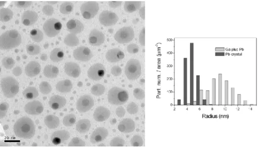
Figure 1 displays the general appearance of the Ga-Pb nanosystem as observed by TEM in the case of sample E1: Ga0.85Pb0.15 corresponding to the successive deposition of layers of
equivalent thicknesses: 3.2nm for Ga and 0.8nm for Pb. We can easily distinguish the uniform contrast of Ga nanodrops and the diffraction contrast of Pb nanocrystals. The Ga nanodrops [7] size distribution is bimodal. In the main mode, whose size is about 20 nm, we observe the presence of Pb crystals of about 8nm in size. Many Pb crystals are in contact with the Ga/SiOx
inner surface while only some of them are in the center of the Ga droplet. In the second mode, the Ga nanodrops are small and polydispersed in size. In this case, the Pb nanocrystals are less visible due to their small size. High resolution observations demonstrate that no free solid Pb crystal is visible outside the Ga droplets.
FIG. 1: Typical picture of a Ga-Pb system (sample E1: Ga0.85Pb0.15) at room temperature, obtained with bright-field TEM. Ga is liquid (uniform light grey) and Pb is solid (more or less dark depending on the orientation of the crystal, in Bragg conditions or not). On right, histogram of Ga and Pb sizes for the same sample (for clarity, Ga droplets of radius < 4nm have not been considered).
of Fig. 1, we can observe 6 facets corresponding to the projection of the Pb cuboctaedron on the plane of the picture. One can easily note that the bigger the Ga droplets, the bigger the Pb crystals inside. The presence of nanodrops containing no Pb crystal is an exception that can be explained by a split of the Ga droplet before being covered by SiOx.
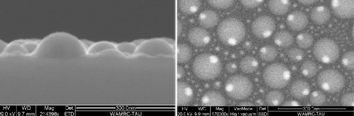
More information on the relative shapes of the Ga droplets and the Pb crystals can be obtained by SEM provided larger particles are used. In Fig. 2 we give a secondary electron image showing the cross-section of a Ga0.951Pb0.049 (Ga25nm + Pb2nm) sample on a silicon substrate
which has been broken in order to reveal the profile of the droplets in a plane normal to the substrate. It is possible to measure the height and the apparent diameter of the Ga droplets in order to derive the contact angle θ of Ga on the SiOx substrate. The word "apparent" refers to the projection of the particle on the image plane. Such an analysis has been performed on two samples Ga0.951Pb0.049 and Ga0.975Pb0.025 (Ga25nm + Pb2nm and Ga50nm + Pb2nm).
FIG. 2: Upper panel: SEM experiments: cross-section (secondary electron image) and planar view of the sample (back-scattered electrons image).
Lower panel: Contact angle on the SiOx substrate versus Ga nanodrops size (from cross-section SEM experiments)
As shown in Fig.2, we do not observe a size dependence of θ. The average value of the contact angle of a nanodrop of Ga on SiOx is found to be θ = 84° ± 2°.
Due to the higher signal of back-scattered electrons from Pb relative to Ga, the back-scattered electron image in Fig. 2 reveals that Pb crystals exist in every droplet, even in the smallest ones.
3. Analysis of the two-components breath figure growth
The growth mode of the Ga liquid breath figure is known [1-2]. Concerning Pb, TEM and SEM observations show that all the Pb is inside the Ga droplets. For understanding the Pb growth it is necessary to analyse the relation between the Ga and Pb particle sizes.
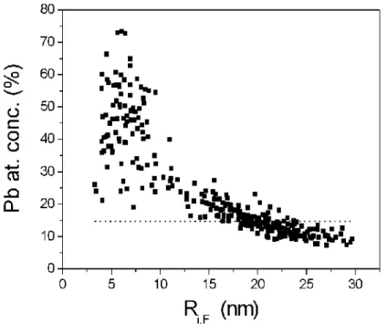
The overall Pb concentration in a given Ga droplet has two contributions: the first one corresponds to Pb dissolved in liquid Ga: it is very small but unknown unless we accept the data of the bulk phase diagram [6] which indicates 0.02 at % at room temperature; the second one is obtained from the visible Pb rich solid phase. By analyzing the TEM pictures at room temperature, we can extract the Pb concentration due to this second contribution as a function of the Ga droplet radius (Fig. 3). A strong decrease of the Pb concentration with the Ga droplets size is observed. The horizontal dotted line corresponds to the concentration one would observe if Pb was uniformly distributed among the Ga particles.
FIG. 3: Pb atomic concentration versus the apparent size of the Ga droplets in Pb0.147Ga0.853 sample. The dotted line corresponds to the average Pb atomic concentration
In order to explain this difference, we present a model that identifies how the Pb atoms share among the Ga droplets and therefore predicts the Pb concentration within each nanodrop. First we have analyzed a Ga breath figure to obtain the size distribution of the droplets versus the thickness (dGa) of the equivalent Ga parallel film. The average apparent radius RGa of the
droplets is given by RGa = 2.48 dGa in the limited size range of the sample [2].
An image analysis of TEM pictures permits to extract the sizes ri of the Pb crystals together
with the sizes Ri of the Ga nanodrops. For a given sample, the volumes Vi Pb
of Pb crystals are calculated in a spherical approximation while for Ga droplets the volumes Vi
Ga
are calculated taking into account the contact angle θ of Ga on the SiOx substrate obtained in
previous paragraph. This results in:
ViGa πRi 3
3f (1)
where Ri is the apparent radius of the Ga droplet and f
sin3θ
2 cos3θ 3cosθ .
The model, which describes the relation between Riand ri, is based on some assumptions on
the growing process: once the Ga breath figure is established, a uniform Pb atoms flux is sent on the sample and all Pb atoms enter into Ga droplets. This aggregation problem has been investigated (see [8] and references therein) and capture zones must normally be defined for determining which island receives a given atom. In the present case the problem is simplified by the fact that initial Ga droplets are known and have a fixed position. We therefore make two simple assumptions based on the two different ways a Pb atom reaches a Ga nanodrop: i) the probability for a Pb atom to directly arrive on a Ga droplet is proportional to the apparent surface of the Ga droplet.
ii) between the Ga droplets, the Pb atoms arriving on the bare SiOx substrate diffuse and finally incorporate in a Ga droplet. In this case its probability to enter a Ga droplet is proportional to the contact line length.
With such assumptions, it is possible to calculate the size of the Pb crystal inside each Ga droplet. In a period of time dt, the total volume of Pb arriving in the particle number i is the sum of the two previously defined contributions:
dViPb dVi Pb, dir
dVi Pb,diff
(2) that can be written as:
π f Ri 2 (t) dRi πRi 2 (t)δPb βRi(t) dt (3)
where δPbis the atomic Pb deposition rate δPbtF dPb, tF being the total Pb deposition time
and β a coefficient related to the size of the capture zone. Integrating between initial (I) and final (F) times gives:
f dPb Ri,F Ri,I β πδPb ln β πδPb Ri,F β πδPb Ri,I (4)
Summing over all nanoparticles the term on the right hand side of equation (3), we obtain the total deposition rate for Pb on the analyzed total surface AT at the time t, that is equal to δPbAT.
For t=tF, the final apparent radii Ri, F satisfy the following equation:
π Ri,F2 i
β δPb Ri,F i
AT (5)For every TEM picture, the β/δPb ratio can be calculated, using measured values for AT and the
Resolution of Eq. 4 gives the initial (i.e. without Pb) apparent radius Ri, I of the Ga droplet i,
the final (i.e. with Pb) apparent radius Ri,F being measured on the TEM picture.
It is then possible to obtain the size ri of the Pb crystal:
4f ri3Ri,F 3
Ri,I 3
(1 C) (6)
where C accounts for the small volume solubility of Pb atoms in the liquid Ga.
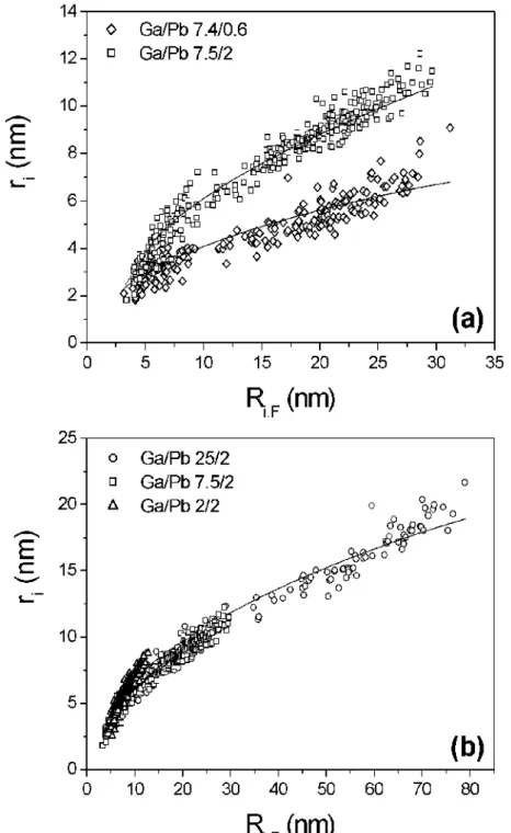
On the Fig. 4, we compare the values of the radii ri of the Pb crystals measured by TEM with
the ones calculated with the above model. Data are represented as a function of Ri,F, the
apparent size of the Ga droplets, also measured by TEM.
Fig.4a presents the results obtained for two samples with same Ga and different Pb contents while Fig.4b gives the results obtained for three samples with same Pb and different Ga contents.
Remember that the value on the ordinate axes in the graphs do not account for the total quantity of Pb in the particle, as can be seen in Eq. (6), but only for the part that is visible as a floating solid crystal of radius ri in TEM pictures. Due to a small amount of Pb atoms
dissolved in Ga, there is a nonzero value of the Pb average concentration in the sample for which there is not Pb crystal formation. This has been actually confirmed in a sample Ga0.9936Pb0.0064 (Pb volume concentration 1% i.e. Ga2nm + Pb0.02nm) for which there was no
evidence of solid cores in HREM images.
4. Discussion
The first question raised by TEM observations is: why is the Pb crystal inside the Ga droplets ? The surface energies of Ga and Pb are known: γGa 690 mJ m
2
and γPb 610 mJ m
2
(see, for instance, [9]); in the lack of more data, we can approximate that interfacial energies γGa /SiO and γPb /SiO are respectively not very different than the surface
energies γGa and γPb. Concerning the interfacial energy γGa / Pb, it is not known but is
certainly much weaker. We are therefore in the situation γGa /SiO γPb /SiO ? γGa /Pb,described by
Hagege and Dahmen [4], which excludes the possibility to have Ga and Pb isolated particles. Moreover, as γGa /SiO and γPb /SiO are not very different one from the other, the same authors
predict a microstructure, in the particles, where both components are separated in two parts Ga and Pb with a plane separation. We observed that situation is more complex because it depends on temperature. A more detailed analysis will be reported in another paper [10].
FIG. 4: The radius r of the Pb crystal (with spherical approximation) versus the apparent radius RF of its embedding Ga droplet. The symbols correspond to experiments listed in the following table. In the model (solid line), the volume solubility of Pb in Ga is C = 1%.
Sample name picture symbol Pb Volume Conc. CPb (%) dPb (nm) dGa (nm) Area AT (µm2) Surface coverage D7: Ga0.95Pb0.05 ◊ 7.5 0.6 7.4 0.337 0.577 C4: Ga0.853Pb0.147 W 21.1 2 7.5 0.547 0.551 A8: Ga0.951Pb0.049 d 7.4 2 25 1.267 0.629 A6: Ga0.61Pb0.39
V
50 2 2 0.113 0.369We obtain a satisfactory agreement between our simple model and the experimental results. As can be seen in Fig. 4, this good agreement is found without any free parameter. It is important to note that the Pb solubility C in Ga has been determined in accordance to our hypothesis that all Pb atoms are incorporated on Ga droplets. The values obtained are roughly one order of magnitude larger than the one given by the bulk phase diagram. We suppose that this disagreement is due to a size effect and is presently investigated.
We present in Fig. 5 the dependence between the surface coverage (i.e. the fraction of the sample covered by nanoparticles) and the mean radius of the nanodrops. We recover the same behavior than the one obtained for a classical one-component breath figure [1-2]. The saturation for the larger Ri,F values is due to the coalescence processes giving rise to the
breath figure geometry. For the lower Ri,F values, it is important to note that the geometric
structure is qualitatively different. This is of great importance when trying to estimate which one of the two possible incorporation processes considered in the model is dominant. In other words, the ratio between the two terms appearing in Eq. (5) is strongly affected by the geometric structure of the system.
FIG. 5: Surface coverage versus average droplet apparent radius for the Ga-Pb samples investigated.
This is illustrated in Fig. 6 where we represent the probabilities pi,1 and pi,2 for an atom to
be absorbed respectively directly or after diffusion on the substrate as a function of the particle radius Ri,F . These probabilities are built using Eq. (3) applied to an experimental
distribution of radius Ri,F presented in the inset. Since we considered that an incident Pb
that : 1 ) ( ,1 ,2
N i i i p pwhere N is the number of Ga droplets. We can see that the two processes have almost the same importance for particles with radius roughly smaller than 15nm. A direct impingement becomes the main process for larger particles. As discussed above, this cross-over is directly associated to the geometric structure of the Ga breath figure. A different geometric structure (e.g. a different radius distribution or a long-ranged correlation between particle centers of mass) would strongly influence the transition between the two regimes.
FIG. 6: The probabilities pi,1 and pi,2 for an impinging Pb atom to enter a Ga nanodrop of radius F
i
R, directly or after diffusion respectively.
5. Conclusion
In this paper, we have demonstrated that it is possible to grow nanocrystals inside a different non-interactive liquid phase if both materials are immiscible. In the present study each Ga nanodrop behaves like a nano-container inside which the Pb crystallization occurs.
For this purpose we have developped a technique which appears suitable: the two-components breath figure. We have identified two distinct growth regimes depending on the way the solute atoms are incorporated in the nanodrop. If the Pb atoms directly reach the nanodrop, we expect a scaling of the concentration as R-2, while if the Pb atoms touch the substrate, the
expected scaling is R-1. A cross-over between these two regimes should occur as a function of
References:
* Corresponding author: kofman@unice.fr
[1] P. Meakin, Rep. Prog. Phys. 55, 157 (1992)
[2] E. Søndergard, R. Kofman, P. Cheyssac and A. Stella, Surface Science 364, 467 (1996)
[3] T. Ben-David, Y. Lereah, G. Deutscher, J.M. Penisson, A. Bourret, R. Kofman and P.
Cheyssac, Phys. Rev. Lett. 78, 2585 (1997)
[4] S. Hagege and U. Dahmen, Phil. Mag. Lett. 74, 259 (1996) [5] A. Defrain, J. Chim. Phys. 74, 851 (1977)
[6] I. Ansara and F. Ajersch, J. Phase Equilibria 12, 73 (1991)
[7] L. Haderbache, R. Garrigos, E. Søndergard, R. Kofman and P. Cheyssac, Surface Science 410, L748 (1998)
[8] A. Zangwill, Nature 411, 651 (2001)
[9] B. Pluis, D. Frenkel and J.F. van der Veen, Surface Science 239, 282 (1990) [10] M. Allione, R. Kofman, F. Celestini and Y. Lereah, Eur. Phys. J. D 52 (2008) 279