Publisher’s version / Version de l'éditeur: Physics in Canada, 54, 8, 1998-01
READ THESE TERMS AND CONDITIONS CAREFULLY BEFORE USING THIS WEBSITE.
https://nrc-publications.canada.ca/eng/copyright
Vous avez des questions? Nous pouvons vous aider. Pour communiquer directement avec un auteur, consultez la
première page de la revue dans laquelle son article a été publié afin de trouver ses coordonnées. Si vous n’arrivez pas à les repérer, communiquez avec nous à [email protected].
Questions? Contact the NRC Publications Archive team at
[email protected]. If you wish to email the authors directly, please see the first page of the publication for their contact information.
NRC Publications Archive
Archives des publications du CNRC
This publication could be one of several versions: author’s original, accepted manuscript or the publisher’s version. / La version de cette publication peut être l’une des suivantes : la version prépublication de l’auteur, la version acceptée du manuscrit ou la version de l’éditeur.
Access and use of this website and the material on it are subject to the Terms and Conditions set forth at
A silicon microtips Field-Emission Display prototype
Py, Christophe; Grant, Peter; Gao, Mae
https://publications-cnrc.canada.ca/fra/droits
L’accès à ce site Web et l’utilisation de son contenu sont assujettis aux conditions présentées dans le site LISEZ CES CONDITIONS ATTENTIVEMENT AVANT D’UTILISER CE SITE WEB.
NRC Publications Record / Notice d'Archives des publications de CNRC:
https://nrc-publications.canada.ca/eng/view/object/?id=6a927290-13c9-45a9-b004-f0749de8a93b https://publications-cnrc.canada.ca/fra/voir/objet/?id=6a927290-13c9-45a9-b004-f0749de8a93b
A silicon microtips Field-Emission Display prototype
Christophe Py, Peter Grant and Mae Gao, Institute for Microstructural Sciences, National Research Council of Canada, Montreal Road, Ottawa Ontario K1AOR6 Canada. Tel: (1)6139930504 Fax: (1)6139525711 e-mail: [email protected] [email protected]
Introduction
Field-Emission Displays are flat-panel displays that retain the intrinsic visual properties of CRTs. For this reason, they are trying to enter the market through applications where the limitations of liquid crystal displays are unacceptable. In the long term, FEDs are expected to also become cheaper and more power-efficient, though the technology is now facing problems such as phosphor lifetime and efficiency as well as the high cost of drivers.
A FED prototype fabrication process developed at IMS is presented. The performances and shortcomings of this device are used as the basis for discussion for what it will take to make it a viable product.
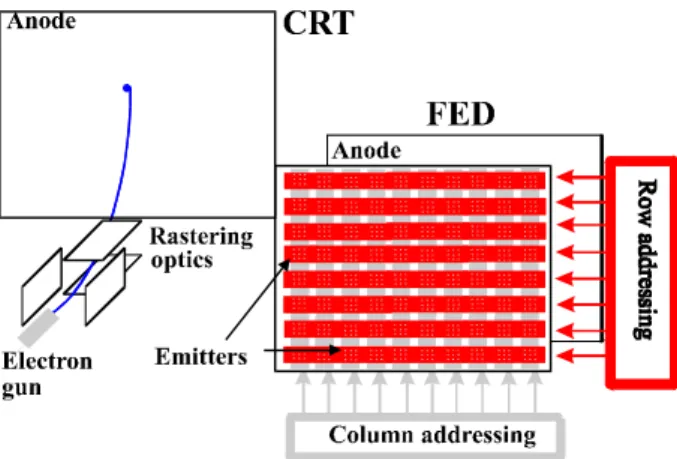
Figure 1: Field-Emission Display principle of operation compared to a Cathode Ray Tube. In a CRT the beam of a single electron gun illuminates the anode pixel by pixel. In a FED micro-emitters are integrated on a plate facing the anode and illuminate the pixel they face when addressed by an XY matrix.
Principle
Images in a FED are obtained, like in a Cathode Ray Tube, by bombarding a phosphor screen with an electron beam. However, in a FED each pixel of the screen receives electrons produced by micro-emitters integrated on a plate and directly facing the pixel, whereas in a CRT the beam of a single electron gun is rastered through all the screen pixel by pixel (Figure 1). Micro-emitters are addressed by an XY matrix and there is no need for deflection optics. The plate on which the emitters are integrated is usually referred to as the cathode, and the screen as the anode. The micro-emitters are microtips surrounded by an extraction gate lying on a thick insulator (Figure 2). When biased at a voltage higher than that of the microtip, the extraction gate produces a very intense field at the apex of the microtip to thin down the Fermi barrier (from the emitter material to vacuum) and permit electrons to tunnel through it. Electrons are then accelerated towards the anode. To form the XY matrix, microtips are grouped in columns and the extraction gate is etched in rows. The display is addressed row by row, which means that all the pixels of a same row can be illuminated at the same time. Assuming that microtips emit for a gate to microtip voltage of 80V, the active row is biased at +50V and pixels will be illuminated at the intersection of that row and columns biased at -30V.
Microtips are usually made of an evaporated metal [1] or etched from silicon [2], though some other materials like GaAs are being evaluated for other applications [3].
Figure 2: Micro-emitters in a FED are composed of a microtip and an extraction gate lying on a thick insulator. 1m emitters will typically emit current when the extraction gate to microtip voltage is about 80V. Pixels are illuminated at the intersection of the active row, biased at +50V and active columns, biased at -30V.
IMS chose silicon because the compatibility of the fabrication process with traditional Integrated Circuit processes offers at least two significant advantages:
being able to use existing IC production lines, and thus limit capital investment. being able to integrate addressing
electronics on the same plate as the emitters. This would solve the problem of connecting the matrix to discrete drivers, which can be a limiting factor in the small and high resolution display market that FEDs are targeting.
Process flow
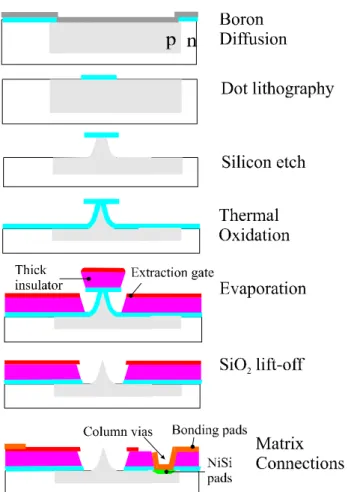
In the past two years, IMS developed a fabrication process for a proof-of-concept prototype cathode based on silicon microtips. As seen in Figure 3, the conical aspect of the microtip is obtained by undercutting silicon under a SiO2 round dot mask. In order to
obtain a microtip with a high aspect ratio, Reactive Ion Etching is preferred to wet etching.
A high aspect ratio microtip is desirable for two reasons:
a large microtip base to gate distance reduces the capacitive coupling and chances of breakdown, and
a small microtip apex to gate distance enables extracting current for a lower gate voltage.
Figure 3: IMS’s silicon microtip fabrication process. The microtip is obtained by under-cutting silicon under a SiO2 dot mask and
consuming the rest of the silicon by thermal oxidation. The dot is kept as a self-aligned mask to deposit the thick insulator and the extraction gate; it is then etched-off. Columns are obtained by thermal diffusion of p type impurities in a n type substrate.
+50V
+20V
+20V
0V
-30V
-30V
Anode Row Column Thick insulatorThe RIE is stopped before the dot falls off and the remaining silicon is consumed by thermal oxidation. This layer provides good electrical insulation between the base of the microtip and the extraction gate. It also permits keeping the dot as a self-aligned mask to evaporate the thick insulator and the extraction gate without compromising the microtip sharpness. After these evaporation steps, the dot is etched-off and the emitter is complete. The Scanning Electron Microscope picture of Figure 4 shows a group of microtips. The initial dot diameter was 1m, and the resulting gate aperture is approximately 1.2m. The radius of curvature at the apex of microtips is estimated between 5 and 10nm, which provides a high field enhancement factor.
Figure 4: SEM top view picture of four emitters. The extraction gate aperture is approximately 1.2m and the radius of curvature of the microtip’s apex between 5 and 10nm.
The integration of emitters in a XY matrix requires etching the extraction gate in rows (not shown in Figure 3) and separating the base of the microtips in columns. Electrical insulation from the n type substrate is achieved by doping columns with p type impurities (Boron). The substrate is grounded so when a column is active (negatively
biased) the p-n junction is reverse-biased and therefore insulating. The junction has to sustain a high reverse voltage (at least -30V) and be several microns deep (microtips are etched in the columns). The columns are obtained in a one step thermal diffusion using thermal oxide as a mask. After forming the emitters, contacts to the columns are made by etching vias through the two oxide layers and depositing nickel silicide pads. Finally, Au connection pads are deposited for rows and columns contacts, and the device is attached in a package as shown in Figure 5.
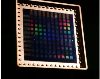
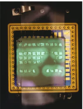
Figure 5: Top view of the packaged cathode. Each pixel is a 1.54mm square containing 20736 microtips. Rows and columns have a 2.54mm pitch.
The prototype, shown in Figure 5, is a 10 row by 10 column array with a very coarse 100mils pitch allowing a simple connection and addressing scheme. From a micro-fabrication point of view, obviously, a much smaller pitch could be attained.
The anode is a glass sheet covered with indium tin oxide, a transparent conductive material, and coated with a ZnO:Zn phosphor powder. ZnO:Zn is known to be a very efficient phosphor at low voltages and is used in vacuum fluorescent displays (used for example in microwave ovens and car stereos). Unfortunately, its very broad spectrum
(whitish green) makes it useless for colour displays. The phosphor is synthesized in-house by reducing a ZnO powder in an hydrogen atmosphere, and deposited by sedimentation from a solvent.
Anode and cathode are mounted together and 1mm apart in a vacuum chamber. The matrix and the anode are connected to addressing electronics controlled by a computer.
Results
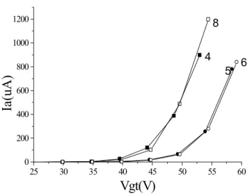
Typical emission characteristics are shown in Figure 6. The anode current is plotted as a function of the gate to microtip voltage for several rows of the same prototype. The anode voltage is found to have very little influence on emission as long as it stays higher than the gate voltage; it was kept at 500V. A current of 1mA can be obtained at a gate to microtip voltage of 53V from a 0.2cm2
emissive area containing about 200,000 emitters. This voltage value is relatively low compared to earlier reports [2,4]. The corresponding 5mA/cm2 current density
meets the requirements of commercial FEDs.
Figure 7 is an anode-side view of the prototype in operation where rows are horizontal and columns vertical. Rows 2,4,5,6 and 8 are working. The other five rows are in short-circuit with the substrate. Deposition of the thick insulator out of a clean-room is probably responsible for a high particle count. Within working rows, some pixels emit far less than others, because emitters were not properly shaped in those places. This is the main reason why rows 5 and 6 seem to have a higher turn-on voltage than rows 4 and 8. Because of their high aspect ratio, the height of microtips is strongly dependent on the initial diameter of the dot. Statistical analysis of dot diameters shows a 6% variation within a sample, which translates into a 500nm height variation and a factor of 10 in emission for identically sharp microtips. The dot lithography is made with a contact aligner, so the precision of the patterning depends on how good the contact between the mask and the sample is and how smoothly the photoresist has been spun. Obviously these steps must be improved to obtain an homo-geneous illumination of the screen. Structures, observed within certain pixels, are partly due to flickering of the emission. Variations in the emitted current reflect interactions (adsorption-desorption and flip-flop) of the apex of microtips with atoms of the remaining gas [5].
Halos are also observed around the pixels: due to the phosphor low transparency (3%), most of the emitted light is trapped between the two plates. A more sophisticated deposition method would produce much thinner phosphors. However, more than 50% of the light would still be emitted toward the
Figure 6: Anode current Ia as a function of the extraction gate to microtip voltage Vgt for several rows of the cathode. The anode voltage is 500V.
25 30 35 40 45 50 55 60 0 200 400 600 800 1000 1200 6 5 4 8
Ia
(u
A
)
Vgt(V)
cathode, not the viewer. In CRTs, this problem is addressed by coating the cathode side of the phosphor with a thin Al mirror layer through which electrons penetrate thanks to their high energy. However, this solution requires an anode voltage at least as high as 5kV [6], not easily obtained in a FED because of a limitation in the cathode to anode distance.
Figure 7: Anode-side view of the operating device. Rows are horizontal, row 1 is on top. Discussion
The fabrication process developed at IMS enables reproducibly obtaining field-effect emission from microtips with a current density satisfactory for display applications. This process also successfully integrates the fabrication of an XY matrix to allow the formation of images.
However, certain shortcomings are observed : Short circuits between the substrate and
extraction gate rows,
Short-circuits between microtips and extraction gate,
Emissivity discrepancy between microtips (many microtips don’t emit at all !), and Variation with time in microtip emission
(flicker).
Two other areas have been identified where improvement must be seen to enhance the performances of FEDs and decrease their price:
High switching voltages [7]: the base of the microtips and the extraction gate form a large capacitance that loads the drivers when switching voltages. As seen in Figure 4, the voltage that must be switched from the off to the on state is not as high as the turn-on voltage. Still, no less than 25V has to be switched on rows and columns. Drivers for these high voltages are expensive, and the reactive power lost in the matrix goes as the square of the switched voltage. Lowering the switched voltage is thus very critical. Low phosphors luminance: even though
emission from a microtip is directive, the beam aperture is still an estimated 15 to 30 solid angle. For a given pixel resolution, this aperture limits the cathode to anode distance. Thus the anode voltage is limited to a value far lower than in a CRT (typically a few 100V compared to 30kV), which dramatically lowers the anode luminance. The fact that FEDs are addressed row by row and not pixel by pixel increases the illumination time by the number of columns (640 in a VGA screen), but the current density still must be increased drastically. This change in the nature of the beam illuminating the anode has lead to research in the synthesis of new families of phosphors [8], but their luminous efficiency and lifetime at high current densities are not yet satisfactory.
Some of the defects observed in IMS’s prototypes, especially short-circuits between the substrate and extraction gate rows and microtip emissivity discrepancy, would be much less dramatic in an industrial environment. Still, the fabrication process has to conciliate a very low acceptance level of visual defects (a few black pixels at best, and a few percent variation in luminance) with the difficulty of obtaining a zero-defect cathode on a large surface. This goal can be attained only if the cathode design is redundant and defect-tolerant. Redundancy is mainly achieved by having a large number of microtips per pixel. Tolerance to short-circuits and emissivity discrepancy requires controlling emitted current pixel by pixel, when drivers can only control it column by column. One solution is to incorporate a resistive layer between the columns and the microtips, which homogenizes the current by decreasing that of most emissive microtips and sustains short-circuits [4]. However, there are advantages in controlling the current by active means, such as transistors, rather than passive devices. IMS is orienting its program in this direction, with a view to integrate more and more of the addressing electronics on the same substrate as the emitters.
In parallel, we are working in two different directions to address the other shortcomings cited above:
Diamond-Like Carbon coatings on microtips: DLC is known to be a very inert material that is expected to have less interaction with residual gases than silicon. Being a very hard material, it is also difficult to etch into microtips, but coating a thin layer on silicon microtips should increase emission stability and emitters lifetime. Moreover, DLC has a lower work function than silicon, and we estimate that it brings a reduction of the switching voltage by a factor of 2 [9].
Simultaneous focusing and deflection: a natural way to enhance the luminance of FEDs is to reduce the aperture of the beam emitted by microtips, allowing an increase in the anode voltage. In some designs, a focusing electrode is added on a separate plate between the cathode and the anode, which results in a very complicated mechanical setup. Integrating a focusing electrode on the cathode [10] is a more elegant solution that IMS is exploring. We have proved by simulations [11] that this focusing electrode can also be used to increase the current density received by the anode without increasing that of the cathode, and multiply the luminance of FEDs by a factor 2.5.
Bibliography
[1] C.A. Spindt, J.Appl.Phys, vol 39 (1968) p3504 [2] K. Betsui, Tech. Digest of the 4th IVMC, Nagahama, Japan, Sept 6-9, 1991, p137
[3] J.L. Shaw et al, Le Vide, Les Couches Minces, Supplt n271 (1994) p124
[4] R. Meyer, Tech. Digest of the 4th IVMC, Nagahama, Japan, 6-9 Sept 1991 p141
[5] C. Py & R. Baptist, J. of Vac. Sci. & Technol. B 12(2), (1994), p685
[6] J. Browning et al, Tech. Digest of the 17th IDRC, Toronto, Canada, Sept. 15-19, 1997, pF-42 [7] R.T. Smith, Tech. Digest of the 17th IDRC, Toronto, Canada, Sept. 15-19, 1997, pF-35
[8] C.J. Summers, Tech. Digest of the 10th IVMC, Kyongju, Korea, Aug. 17-21, 1997, p244
[9] J.A. Dobrowolski et al, Physics in Canada, 54(5) (1996) p207
[10] Y. Yamaoka et al, Tech. Digest of the 9th MPC, Kitakyushu, Japan, July 8-11 1996
[11] C. Py & P. Grant, Tech. Digest of the 17th IDRC, Toronto, Canada, Sept 15-19, 1997, p327