HAL Id: tel-03222108
https://tel.archives-ouvertes.fr/tel-03222108
Submitted on 10 May 2021HAL is a multi-disciplinary open access archive for the deposit and dissemination of sci-entific research documents, whether they are pub-lished or not. The documents may come from teaching and research institutions in France or abroad, or from public or private research centers.
L’archive ouverte pluridisciplinaire HAL, est destinée au dépôt et à la diffusion de documents scientifiques de niveau recherche, publiés ou non, émanant des établissements d’enseignement et de recherche français ou étrangers, des laboratoires publics ou privés.
Ultrafast dynamics of excitons and charge carriers in
colloidal perovskite nanostructures studied by
time-resolved optical spectroscopies
Carolina Villamil Franco
To cite this version:
Carolina Villamil Franco. Ultrafast dynamics of excitons and charge carriers in colloidal perovskite nanostructures studied by time-resolved optical spectroscopies. Chemical Physics [physics.chem-ph]. Université Paris-Saclay, 2020. English. �NNT : 2020UPASF012�. �tel-03222108�
Ultrafast dynamics of excitons and
charge carriers in colloidal
perovskite nanostructures studied
by time-resolved optical
spectroscopies
Thèse de doctorat de l'université Paris-Saclay
École doctorale n° 571, Sciences chimiques : molécules, matériaux,
instrumentation et biosystèmes (2MIB)
Spécialité de doctorat: Chimie
Unité de recherche : Université Paris-Saclay, CEA, CNRS, LIDYL, 91191, Gif-sur-Yvette, France. Référent : Faculté des sciences d’Orsay
Thèse présentée et soutenue à Saclay, le 30/09/2020, par
Carolina VILLAMIL FRANCO
Composition du Jury
Emmanuelle DELEPORTE
Professeure des Universités, ENS Paris-Saclay (LUMIN), Orsay, France
Présidente du jury
Ferdinand GROZEMA
Professeur, Delft University of Technology, Delf, The Netherlands
Rapporteur & examinateur
Dmitry ALDAKOV
Chargé de recherche CNRS (HDR), CEA Grenoble (SyMMES/STEP), France
Rapporteur & examinateur
Benoit MAHLER
Chargé de recherche CNRS, Université Claude Bernard Lyon (ILM),
Villeurbanne, France
Examinateur
Thomas GUSTAVSSON
Directeur de recherche CNRS, CEA Saclay (LIDYL), Gif-sur-Yvette, France
Directeur de thèse
Elsa CASSETTE
Chargée de recherche CNRS, CEA Saclay (LIDYL), Gif-sur-Yvette, France
Co-encadrante & Examinatrice
Thèse de doctorat
NNT
:
2020
To the memory of my father – to whom I dedicate this dissertation, you encouraged me to pursue my dreams and be myself before you left this world.
ACKNOWLEDGMENTS
I would like to express my deepest and sincerest gratitude to my supervisor, Dr. Elsa Cassette for her invaluable guidance and continuous support through this journey. Without her patient instruction, knowledge and enthusiasm, I could not have finished this manuscript on time. My truthful acknowledgments also go to my thesis director Dr. Thomas Gustavsson for his supervision, critical reading of the manuscript and remarks during the past years. Both of you dedicated considerable amount of time during our discussions which contribute to my professional growth as scientist.
I would like to thank my reporters: Ferdinand Grozema and Dmitry Aldakov for their insightful reports and questions. Also, the examinators: Emmanuelle Deleporte and Benoît Mahler for reading this manuscript. Finally, I would like to thank our collaborators: Christian Cornaggia, for his interesting talks effort to have the laser in optimal conditions, as well, Benoît for the discussions on the perovskite nanoplatelets stabilization and characterization. I want to give special thanks to the other members of DICO lab (Gerard, Stephane, Caroline, Dimitra, Akoz, Roberto, Sandrine) not only for the academical discussions, assistance in the administrative duties and enriching talks about French culture but also for your kindness. For sure, it was a pleasure to share the lunch time with all of you. Thank you very much to the graduated students and postdocs (Lara, Behnaz, Valentin, Vangelis, Houda, Jean Michel, Gina) for sharing their experiences and valuable advices.
I cannot forget my toxic homeless friends (Aninda, Rafa, Ben, Sandra, Kamila, Simona, Vir, Fer, Albertito, Dyvia, Livya, Oscar, Malik, Sofi, Lomello, Alex) for all the fun and adventures we had together. Also, my serious tennis friends who know well how to release our PhD stress (Shatha, Roberto, Sven, Dominic, Ahmed, Thomas, Hector) you were like
a light/fire/heater in the middle of a dark forest, cold mountains and tennis courts during winter. Finally, to my friends de la U (Rubencho, Paula, Tefa, Vicky, Steven, Jairo, Diego, …) to resist my madness even without knowing what I was doing in Paris. My cousins (Maleja, Diana Paola, Juanda, Christian, Sebas, Samuel, …) and all my family members for your support through all my life, I hope one day to be an inspiration of persevering as you have been for me every day. Finally, 50% of the credit goes to my mother and sister to keep my motivation, confidence and focus during this time. You both are my strength; in spite of our recent losses you have showed me that together we can always find a way to continue regardless of adversities. I won’t give up just because you are with me.
ABSTRACT
Halide perovskites have emerged as very promising photoactive materials due to their outstanding optoelectronic properties combined with low-cost processability. In spite of their successful implementation in photovoltaic or light-emitting devices, a deep understanding of the dynamics of relaxation and recombination is still missing in order to enhance the device performances. For instance, the single junction solar cells with power conversion efficiencies beyond the Shockley Queisser limit (~ 33%).
This thesis focuses on the study of two major fundamental processes occurring in colloidal halide perovskite nanostructures: the hot charge carrier/exciton relaxation (“cooling”), after excitation above the optical bandgap, and the non-radiative Auger recombination, taking place after high-fluence or high-photon energy excitation. In particular, time-resolved photoluminescence and femtosecond transient absorption spectroscopy were used to investigate the confinement and composition effects in strongly confined two-dimensional (2D) lead iodide perovskite nanoplatelets (NPLs), those were synthesized following the development and optimizations of colloidal methods such as hot injection and ligand assisted reprecipitation (LARP).
For the investigation of the cooling dynamics, a global analysis method based on single value decomposition was used, where the temporal evolution of the spectral lineshapes was modeled with a sequential kinetic scheme. This method was successfully applied to effectively describe the continuous energy relaxation in weakly-confined thick FAPbI3
nanoplates (FA=formamidinium) and allowed disentangling the hot phonon bottleneck from the Auger reheating effects at high excitation fluence. Furthermore, the global analysis was essential to investigate the cooling dynamics in strongly confined 2D NPLs presenting large Stark effects and discrete excitonic band-edge transition far away from
the continuum of states (exciton binding energy in several hundreds of meV). As in the weakly confined samples, the cooling rate of the NPLs decreases with the excitation fluence. However, it is faster in more-strongly confined samples, evidencing the absence of an intrinsic phonon bottleneck. Furthermore, the cooling rate and its evolution with the exciton density were found independent of the nature of the internal cations (FA, MA=methylammonium and Cs=cesium). However, when comparing with the rate measured in 2D layered perovskite thin film with equivalent quantum well thickness, the results strongly suggest a role of the surface ligands in the possibility to release the excess energy to the surrounding environment. This suggest that the ligand-mediated relaxation mechanism previously proposed for the exciton relaxation in other colloidal systems can be dominant in the thinner NPL samples with enhanced exciton/ligand vibrational mode coupling.
Then, the multiple exciton recombination dominated by non-radiative Auger recombination (AR) was studied in the strongly-confined 2D perovskite NPLs. Due to the large asymmetric geometry and the limited exciton wavefunction delocalization, the AR rate strongly depends on the exciton density via the initial average inter-exciton distance. At low fluence, this distance is in several tens of nanometers such as the AR is limited by the exciton diffusion in the 2D plane. It thus occurs on a timescale of several hundreds of picoseconds and depends on the sample dimensionality (thickness and lateral sizes). In contrast, high excitation fluences produce “overlapping” excitons with inter-exciton distances of only a few times the exciton Bohr radius, resulting in AR times of less than 10 ps and independent of the NPL composition nor geometry. Finally, the exciton population dynamics of 2D NPLs after excitation in the ultraviolet was measured. The strong dependence of the AR with the inter-exciton distance allows the identification of multiple exciton generation (MEG), which involves the reaction of “geminate biexcitons” produced by the absorption of a single high-energy photon.
Résumé en français
Les matériaux semiconducteurs de pérovskite halogénée se sont révélés très prometteurs en raison de leurs propriétés exceptionnelles et de leur capacité d’élaboration à faible coût. Malgré les progrès réalisés, une meilleure compréhension des dynamiques de relaxation et de recombinaison dans ces matériaux photo-actifs est nécessaire afin d’améliorer les performances des dispositifs opto-électroniques. Par exemple dans les cellules solaires à simple jonction avec un performance de conversion d'énergie supérieure à la limite théorique Shockley Queisser (~33%).
Cette thèse porte sur la relaxation des porteurs de charge/excitons « chauds » après excitation au-dessus de la bande interdite, et la recombinaison Auger advenant après une excitation de forte puissance ou à haute énergie. La spectroscopie de fluorescence résolue en temps et d'absorption transitoire (AT) femtoseconde sont utilisées afin d’étudier les effets du confinement et de la composition sur ces processus, en particulier dans les nanoplaquettes (NPLs) colloïdales de pérovskite bidimensionnelles (2D), dont la synthèse a été développée et optimisée au préalable. Les méthodes utilisées ici sont communément reconnues comme: injection à chaud et re-précipitation assistée par ligand (LARP).
Les dynamiques de relaxation ont été étudiées par AT en utilisant une méthode d'analyse globale où l'évolution temporelle des différentes compositions spectrales est modélisée suivant une cinétique de réactions séquentielles. Cette méthode a pu être appliquée afin de décrire efficacement la relaxation progressive dans les nanostructures de FAPbI3 (FA=
formamidinium) faiblement confinées, et a permis de dissocier les processus de retardement de relaxation à haute puissance d’excitation dus aux effets de « hot phonon bottleneck » et de ré-excitation par recombinaison Auger (RA). Par ailleurs, l'analyse globale de l’évolution spectrale a été essentielle afin d’examiner les dynamiques de
relaxation dans les NPLs 2D à fort confinement quantique et diélectrique, présentant des effets Stark importants et une transition de bord de bande excitonique discrète. Comme dans les systèmes faiblement confinés, le taux de relaxation dans les NPLs diminue avec la puissance d'excitation. Cependant, il est plus rapide dans les systèmes présentant un confinement plus important, mettant alors en évidence l'absence de ”phonon bottleneck” intrinsèque. La nature des cations internes (FA, MA=méthylammonium ou Cs) n’influe pas ce taux, ni son evolution en puissance. Toutefois, les mesures dans les films de pérovskite 2D présentant une épaisseur de puits quantique équivalente, suggèrent un rôle des ligands de surface dans la capacité à libérer l'excès d'énergie dans l'environnement. Ce mécanisme de relaxation à médiation par ligand proposé précédemment pour la relaxation de l'exciton dans d'autres systèmes colloïdaux peut être dominant dans les échantillons NPL plus minces avec un couplage de mode vibrationnel exciton / ligand.
Ensuite, les recombinaisons multi-excitoniques dominées par la RA non radiative ont été étudiées dans les NPLs de pérovskite 2D fortement confinées. Dû à la géométrie asymétrique de ces nanostructures et de la délocalisation limitée de l'exciton, le temps de RA dépend fortement de la densité d'excitons via la distance inter-exciton moyenne : A faible puissance d’excitation, la RA est limitée par la diffusion de l'exciton dans le plan 2D et se produit sur plusieurs centaines de picosecondes (dépendant ainsi de la géométrie de l'échantillon). En revanche, une puissance d'excitation élevée produit des excitons dont les fonctions d’onde se recouvrent spatialement, entraînant des temps de RA inférieurs à 10 ps. Finalement, les dynamiques excitoniques dans les NPLs 2D ont été mesurées par AT après excitation dans l’ultraviolet afin d'observer le processus de multiplication d’excitons. Ce dernier implique la génération de plusieurs excitons “géminés”, et donc proches spatialement, suite à l'absorption d'un unique photon de haute énergie.
i
CONTENTS
INTRODUCTION ... 1 Aim of research ... 4 Thesis outline ... 5 1. FUNDAMENTAL CONCEPTS ... 81.1. HALIDE PEROVSKITE MATERIALS ... 9
1.1.1. Bulk perovskites ... 9
1.1.1.1. Perovskite crystalline structure ... 9
1.1.1.2. Properties of 3D (bulk) lead halide perovskites ... 10
1.1.2. Confined lead halide perovskites ... 12
1.1.2.1. Quantum confinement ... 12
1.1.2.2. Perovskite colloidal nanocrystals: from 3D to 0D materials ... 17
1.1.2.3. 2D layered perovskites ... 19
1.2. DYNAMICAL PROCCESSES IN SEMICONDUCTOR NANOCRYSTALS .. 26
1.2.1. Introduction ... 26
1.2.2. Hot charge carrier & hot exciton relaxation: cooling... 28
1.2.2.1. Classical model of energy loss-rate ... 28
1.2.2.2. “Hot phonon bottleneck” at high excitation fluence ... 29
1.2.2.3. “Intrinsic phonon bottleneck” in strongly confined systems ... 29
1.2.3. Non-radiative Auger recombination ... 32
1.2.4. Multiple exciton generation ... 33
1.2.5. Radiative and non-radiative exciton recombination ... 35
1.2.6. Conclusion ... 36
REFERENCES ... 37
CHAPTER 2. EXPERIMENTAL METHODS ... 46
2.1.OPTICALSPECTROSCOPYTECHNIQUES ... 47
2.1.1. Steady-state optical spectroscopy ... 47
2.1.1.1. Absorption spectroscopy ... 47
2.1.1.2. Photoluminescence spectroscopy ... 48
2.1.2. Time-resolved optical spectroscopy ... 50
2.1.2.1. Pulsed laser excitation sources ... 50
2.1.2.2. Time-resolved photoluminescence (TR-PL) ... 51
2.1.2.3. Femtosecond transient absorption spectroscopy (fs-TA) ... 57
ii
2.2.SYNTHESISOFCOLLOIDALPEROVSKITENANOSTRUCTURES ... 80
2.2.1. Introduction to the wet chemical methods ... 80
2.2.1.1. Hot-injection (HI) method ... 81
2.2.1.2. Ligand-assisted re-precipitation (LARP) method ... 84
2.2.2. Experimental syntheses protocols developed ... 88
2.2.2.1. Synthesis of weakly confined FAPbI3 nanosystems. ... 88
2.2.2.2. Synthesis of the strongly confined FAPI nanoplatelets ... 92
2.2.2.3. LARP method extended to the synthesis of CsPI and MAPI NPLs ... 99
ANNEXE 2. ... 107
REFERENCES ... 111
CHAPTER 3. HOT CHARGE CARRIER AND EXCITON RELAXATION IN COLLOIDAL PEROVSKITE NANOSTRUCTURES ... 117
3.1. Introduction ... 118
3.2. Carrier relaxation in weakly confined FAPbI3 nanostructures ... 120
3.2.1. Classical method of the tail-fitting to extract Tc ... 122
3.2.2. Global analysis of TA data ... 124
3.2.2.1. Short-time dynamics ... 124
3.2.2.2. Middle and long-time dynamics ... 130
3.2.3. Conclusion: Global analysis method ... 133
3.3. Hot exciton cooling in strongly-confined 2D nanoplatelets ... 134
3.3.1. Transient absorption experiments in FAPI n=2 nanoplatelets ... 134
3.3.1.1. Description of the TA data ... 134
3.3.1.2. Kinetic model of relaxation in strongly confined 2D perovskites ... 138
3.3.2. Comparison of the cooling dynamics in different nanostructures. 147 3.3.2.1. Confinement effect ... 147
3.3.2.2. Cation effect: hybrid versus fully-inorganic n=2 NPLs ... 149
3.3.2.3. Ligand effect: colloidal nanoplatelets versus 2D thin films ... 150
ANNEXE 3. ... 155
iii
CHAPTER 4. AUGER RECOMBINATION AND MULTIPLE EXCITON GENERATION IN STRONGLY CONFINED COLLOIDAL 2D PEROVSKITE
NANOPLATELETS ... 167
4.1. Introduction ... 168
4.2. Colloidal NPL samples and characterizations ... 169
4.3. Time-resolved photoluminescence experiments ... 171
4.3.1. Assignment of the multiple- and single- exciton dynamics ... 172
4.3.2 Discussion on the kinetics of the multi-exciton dynamics ... 175
4.4. Visible transient absorption spectroscopy experiments ... 181
4.4.1. Diffusion- limited exciton-exciton recombination and intrinsic Auger rate ... 185
4.5. Multiple exciton generation (MEG). ... 188
ANNEXE 4 ... 196
REFERENCES ... 202
GENERAL CONCLUSION ... 207
1 INTRODUCTION
Metal halide perovskite materials have attracted an enormous scientific interest in recent years. The optical and electronic properties such as high optical absorption coefficient, large defect tolerance, long diffusion lengths combined with low-cost and solution processability, contribute to their successful implementation in several photonic devices [1–5].
Over the last 10 years, solar cells based on bulk perovskite materials have turned out to be the technology with the most remarkable improvement among all emerging photovoltaics technologies (see Figure 0.1). For instance, technologies based on organic materials have been the subject of intense research for much longer time without attaining the comparable efficiencies. For example, dye-sensitized solar cells (DSSC) were introduced about 30 years ago, but the highest power conversion efficiency (PCE) is still limited to about 12 % and organic photovoltaics (OPVs), which emerged about 20 years ago attains 18 %. In contrast, new nanostructured semiconductors materials such as quantum dots (QDs) have almost reached a 20 % level in around 10 years. However, so far perovskite is the only material able to compete with conventional silicon technologies reaching efficiencies of about 25 %. Interestingly, perovskite/Si tandem cells show PCE values around 30 %, which is very promising.
2
Figure 0.1. Best research-cell efficiency chart from NREL.
https://www.nrel.gov/pv/cell-efficiency.html. The performance of perovskite solar cells is highlighted.
In spite of these outstanding performances and the many attempts to decreases the losses on the devices, there is a fundamental thermodynamic limit, which hinders single-junction solar cells to reach a power conversion efficiency (PCE) of 100 %. This limit is known as the Shockley-Queisser (S-Q) limit stipulating that the maximum PCE of any single junction solar cell is 33 %. This value is obtained considering charge carriers fully equilibrated with the lattice in a single active semiconductor layer where the valence and conduction bands are separated by a bandgap energy (Eg). There are two fundamental
mechanisms hindering the efficient photon to current conversion that are the
transmission and the relaxation losses, as shown in Figure 0.2. Simply speaking, for the
optimize bandgap material, only one third of the absorbed sunlight photons generate charge carriers, 18 % of the photons pass right through the solar cell (not absorbed) and 47 % of the photons turn into heat (http://solarcellcentral.com/limits_page.html).
3
Figure 0.2. Main principal sources of losses for a silicon semiconductor (bandgap 1.1 eV) through
the solar spectrum (top line). Considering the Shockley-Queisser limit for single-junction solar cells. The thermalization (i.e. relaxation here) represents the largest loss, and increases for the high-energy region of the solar spectrum. Adapted from https://spie.org/news/4146-multiple-exciton-generation-in-a-quantum-dot-solar-cell?SSO=1
The transmission losses are due to the fixed character of Eg: all photons with an energy
below this value are not absorbed by the material. The relaxation losses are due to the fact that photons with an energy above Eg create a hot charge carrier population
susceptible to release its excess energy as heat (smaller voltage reached). This process occurring in only a few hundreds of femtoseconds is also known as cooling. The timescale of this undesired ultrafast process is usually at least one order of magnitude faster than the typical carrier extraction times (on the picosecond time range). The ultimate PCE limit could be increased from about 33 % to about 66 % if the hot charge carriers could be extracted before losing their excess energy as heat [7].
Another consideration of the S-Q limit calculation is that one photon can produce just a single electron-hole pair. Considering that sun light also contains high-energy photons that can be several times Eg of the semiconductor material, it is in principle possible to
4
generate several electron-hole pairs from one high-energy photon. This process is known as carrier multiplication (CM). In this case, the PCE could be increased to 44 % (still assuming that rapid relaxation losses occur).In order to explore non-conventional approaches to overcome the Shockley-Queisser limit, nanoparticles have been proposed as candidates to enhance both the collection of high-energy (hot) charge carriers and to increase the current by CM. The major reason is that in nanostructures the quantum confinement increases radically the spacing between the electronic levels and thereby is expected to slow down the cooling rate (bottleneck effect, discussed in Chapter 3). Moreover, carrier multiplication is also increased in nanostructures due to the enhanced Coulomb interactions and the relaxation of the momentum conservation.
Alternatively, the colloidal nanostructures of lead halide perovskites also represent a promising material for light emitting devices such as LEDs or lasers, due to their high luminescence quantum yield and tunable narrow-band emission. In addition, the fact that the electron-hole pairs are more strongly bound to form excitons in nanoparticles helps the radiative recombination. However, non-radiative pathways such as multiexciton
Auger recombination at high exciton density are also enhanced in small nanoparticles
where the interactions between excitons are more pronounced. In such a case, the energy liberated from the exciton recombination process is transferred to an extra carrier, decreasing the efficiency in light emitting devices such as LEDs and lasers. In spite of this, the Auger recombination process has been poorly studied in colloidal perovskite systems with different morphology and dimensions. Particularly, strong confined perovskite materials such 2D nanoplateles.
Aim of research
The aim of the present thesis is to study the effects of the quantum confinement and the chemical composition on the ultrafast non-radiative processes occurring in colloidal perovskite nanostructures relevant for photonic devices such as nanostructured solar
5
cells, LEDs, lasers and photo-detectors. Charge carrier cooling, Auger recombination and multiple exciton generation depend on the initial charge carrier density as well as the excitation photon energy. Consequently, we investigate the ultrafast dynamics of these systems under different excitation conditions using time-resolved optical spectroscopy techniques such as time-resolved photoluminescence and femtosecond transient absorption.
Thesis outline
The thesis is organized in 4 chapters as follow:
Chapter 1: This chapter introduces the fundamental concepts necessary to the understanding of this thesis. We first describe in detail the halide perovskite materials. We discuss the relation between structure and function with a special emphasis on the origin of their unique optical properties. More precisely, we discuss the effects of quantum confinement on the electronic structure and the optical properties. Secondly, we discuss the different dynamical processes occurring in confined semiconductor systems in general. A special attention is given to the charge carrier cooling, Auger recombination and
multiple exciton generation process and how these are modulated by the dimensionality
of the nanostructures.
Chapter 2: A detailed description of the experimental methods, the spectroscopic techniques and synthetic protocol employed in this thesis, is given. A femtosecond transient absorption setup was specifically constructed and adapted for the experimental studies of this thesis. In addition, a conventional time-resolved photoluminescence technique was used in order to obtain complementary information. We then describe the
6
synthesis and the characterization of the perovskite nanostructures studied here. A particular attention is given to control their morphology and chemical constitution.
Chapter 3: In this chapter, we study the hot charge carrier/exciton relaxation to the band-edge (i.e. cooling) in weakly- and strongly confined perovskite nanostructures. In large FAPbI3 nanocrystals in which the main species are free charge carriers, the cooling
dynamics can be extracted by the conventional high-energy tail-fitting method. For the strongly confined 2D perovskite nanoplatelets, in which the main species are excitons, this approach fails due to discretization of the states. We propose an alternative and systematic method, based on the global data analysis and lineshape spectral analysis, to extract the full cooling dynamics. We investigate the effect of the excitation fluence and confinement effects and discuss the absence of an “intrinsic” phonon bottleneck in these strongly confined nanoplatelet systems.
Chapter 4: In this chapter, we study the non-radiative multiexcitonic Auger recombination process in strongly confined 2D nanoplatelets of different chemical compositions and thicknesses. We highlight the deviation from the expected bimolecular recombination and the effects of exciton diffusion on the timescale of the Auger recombination for moderate excitation fluence generating excitons spaced by tens of nanometers. Finally, we present strong indications for multiple exciton generation ocurring in the 2D nanoplatelets when excited with high photon energy and discuss the energy threshold found in the UV region.
REFERENCES
[1] Y. Fu, H. Zhu, J. Chen, M.P. Hautzinger, X.Y. Zhu, S. Jin, Metal halide perovskite nanostructures for optoelectronic applications and the study of physical properties,
7
Nat. Rev. Mater. 4 (2019) 169–188. https://doi.org/10.1038/s41578-019-0080-9. [2] S. Adjokatse, H.H. Fang, M.A. Loi, Broadly tunable metal halide perovskites for
solid-state light-emission applications, Mater. Today. 20 (2017) 413–424. https://doi.org/10.1016/j.mattod.2017.03.021.
[3] W. Zhang, G.E. Eperon, H.J. Snaith, Metal halide perovskites for energy applications, Nat. Energy. 1 (2016) 1–8. https://doi.org/10.1038/nenergy.2016.48. [4] B.R. Sutherland, E.H. Sargent, Perovskite photonic sources, Nat. Photonics. 10
(2016) 295–302. https://doi.org/10.1038/nphoton.2016.62.
[5] L. Protesescu, S. Yakunin, S. Kumar, J. Bär, F. Bertolotti, N. Masciocchi, A. Guagliardi, M. Grotevent, I. Shorubalko, M.I. Bodnarchuk, C.-J.J. Shih, M. V. Kovalenko, No Title, ACS Nano. 11 (2017) 3119–3134. https://doi.org/10.1021/acsnano.7b00116.
[6] M.C. Beard, Multiple Exciton Generation in Semiconductor Quantum Dots, J. Phys. Chem. Lett. 2 (2011) 1282–1288. https://doi.org/10.1021/jz200166y.
[7] A.J. Nozik, Spectroscopy and hot electron relaxation dynamics in semiconductor quantum wells and quantum dots, Annu. Rev. Phys. Chem. 52 (2001) 193–231. https://doi.org/10.1146/annurev.physchem.52.1.193.
8 1. FUNDAMENTAL CONCEPTS
This chapter is divided in two parts. The first part introduces the crystalline structure, composition and dimensionality of the halide perovskite materials and its relation with electronic and optical properties. The different morphologies available of this semiconductor material are stablished to explain concepts such as the quantum confinement effects and the presence of charge carriers and/or excitons in the low dimensional perovskite nanostructures studied here: the weakly confined colloidal perovskite nanoparticles (quasi-3D nanocrystals) and the strongly confined 2D colloidal perovskite nanoplatelets.
The second part deals with the main ultrafast processes taking place in colloidal semiconductor nanostructures after photo-excitation. Initially, the hot exciton/charge carrier relaxation (“cooling”) at high-energy photon excitation occurring in the order of hundreds of femtoseconds. Then, the non-radiative charge carrier/multiexciton recombination (Auger recombination) arising at high-density excitation is discussed. Likewise, the carrier multiplication or multiple exciton generation that could take place in the semiconductor nanostructures when the excitation photon energy is higher than twice the optical bandgap energy and competing directly with the exciton cooling is described. Finally, the radiative and non-radiative electron-hole pair recombination usually happening in few to tens of nanoseconds.
9 1.1. HALIDE PEROVSKITE MATERIALS
1.1.1. Bulk perovskites
1.1.1.1. Perovskite crystalline structure
Perovskite is a large class of materials with an ionic crystalline structure analogous to the oxide CaTiO3 and represented by the chemical formula ABX3, where A and B are two
different cations and X, an anion. Among them, halide perovskites with the Xpositions occupied by halide anions such as chloride (Cl-), bromide (Br-) and iodide (I-) and where
B2+ is a divalent transition metal as lead (Pb2+) or tin (Sn2+), have recently emerged as
promising photoactive materials for various optoelectronic applications. In this case, the structure consists in the arrangement of corner-sharing [BX6]4- octahedron, with a
monovalent A+ cation located in the space formed in the center of the 8 octahedra, as
depicted in Figure 1.1.
The nature of the A+ cations that can fit into this cavity is limited by the Goldschmidt’s
tolerance factor to conserve the structural stability [1]. In the case of fully inorganic perovskite, A+ corresponds to an atomic cation, usually cesium (Cs+), while in the case of
hybrid organic-inorganic perovskite, the small organic cations can be methylammoniums (CH3NH3+, or MA+) or formamidiniums (CH(NH2)2+, or FA+). Halide perovskites structure
usually deviate from the ideal cubic phase and present several polyforms depending on the temperature and composition. For example, in the well-known MAPbI3 perovskite, as
the temperature decreases, the octahedral lattice framework is distorted, which results in the change of the crystallographic structure from cubic at high temperature (T > 327 K), to tetragonal at room temperature, then to orthorhombic at low temperature (T < 162 K) [2]. The defined phase transitions for the different perovskite compositions are well-described in several recent reviews [1,3,4] .
10
The ionic character of the lattice allows a high crystallinity of the perovskite materials at room- or fairly low temperatures. This enables processing on a range of substrates with different morphologies such as single- or poly-crystalline thin films, the growth of macroscopic single crystals, or the synthesis of colloidal nanocrystals dispersed in an non-polar organic solvent. However, the ionic character of the perovskite structure also causes a high chemical instability to moisture, air exposure, light and temperature [4].
Figure 1.1. (a) Schematics of the halide ABX3 perovskite crystal structure adapted from reference [5]. (b) Tunability of the halide perovskite emission peak with their chemical composition, reproduced from reference [4].
1.1.1.2. Properties of 3D (bulk) lead halide perovskites
Electronic and optical properties
Halide perovskite materials are direct band-gap semiconductors with a high linear absorption coefficient1 (≈105 cm−1 in their optimum energy range). The band structure of
lead halide perovskites has been calculated by Even and co., including the spin-orbit coupling [6]. The conduction band minimum (CBM) is mainly composed by the p-orbitals of Pb and valence band maximum (VBM) by the p-orbitals of the halide [7,8]. Thus, the halide composition strongly affects the bandgap energy, while the nature of the A+ cations
1 The linear absorption coefficient µlin (cm-1) in perovskite nanocrystals is comparable or larger than classical
inorganic semiconductor materials. While, this µlin value is also comparable in organic semiconductor material,
11
contributes in much less proportion, indirectly via the distortion of the crystalline lattice [9]. For instance, changing the halide from MAPbI3 to MAPbBr3 notably shifts the
absorption onsets from 800 nm to 570 nm and vice-versa. Replacing the MA+ cations in
MAPbI3 perovskite with Cs+, which is smaller in size, increases the wavelength
corresponding to the bandgap from 700 to 716 nm, while the replacement with the slightly larger FA+ cations decreases the bandgap to 838 nm. Additionally, the possibility to have
different halides within the structure in the called “mixed halide perovskite” gives to this material a continuous bandgap tunability [10]. The effect of the nature of the cation and the metal on the optical properties of the halide perovskites is shown in Figure 1.1b, where it can be seen that the emission ranges from the deep blue to the infrared. This thesis focuses on the iodide-based perovskites which presents the lowest bandgap energy, in order to access various energy excitations. In spite of the fact, that perovskite nanostructures present an increased bandgap due to the quantum and dielectric confinement (see sub-sections 1.2.1 and 1.2.3).
Free charge carriers as the main excited species
Upon the absorption of a photon with an energy at least equal to the bandgap, an electron from the valence band is promoted to the conduction band, leaving behind an effective particle with positive charge, a hole. Thus, an electron-hole (e-h) pair is created within the semiconductor. When the two charge carriers are bound by the Coulombic interaction, this bound e-h pair is considered as a quasi-particle known as an exciton. There two parameters to characterize an exciton: the energy needed to dissociate it into free charge carriers (free electron and hole), called the exciton biding energy (Eb) and the distance
between the two charge carriers, known as the exciton Bohr radius (aB).
The exciton binding energy is an intrinsic property of the material, which depends on its composition and dimensionality. The precise determination of Eb in halide perovskites is
12
still debated due to the indirect methods used to estimate it, such as the temperature-dependent photoluminescence, optical and magneto-absorption spectroscopy [11]. However, it is now commonly accepted that Eb is small in bulk lead halide perovskite
materials, ranging from several to few tens of milli-electron volts (meV). As a result, the exciton rapidly dissociates into free charge carriers (electron and hole) at room temperature (RT), where Eb is smaller than the thermal fluctuation energy (kBT ~ 25 meV)
[12]. This is particularly true when decreasing the perovskite bandgap energy, for example from chlorine to iodine. The low Eb in perovskite bulk semiconductors is one of
the reasons for the good electric conductivity of the material and its remarkable charge transport properties. This facilitates notably the charge carrier collection, which is highly desired for photovoltaic devices.
1.1.2. Confined lead halide perovskites 1.1.2.1. Quantum confinement
A system can be considered to be quantum-confined when the electronic and optical properties become size dependent on the microscopic level. This happens when at least one dimension of the material becomes comparable or lower than the exciton Bohr radius (aB), which is typically in the nanometer range.
13
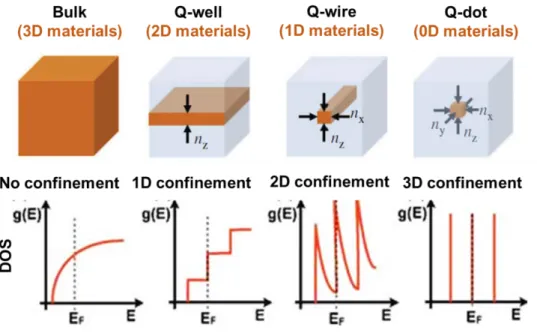
Figure 1.2. Effect of the quantum confinement on the electronic density of states g(E) for
different dimensionalities, from 3D to 0D systems. Adapted from [13].
System dimensionality and density of states
The dimensionality of a system can be defined as a function of the degree of confinement, as shown in the Figure 1.2. In non-confined systems, such as three-dimensional (3D) materials, the charge carriers are free to move in all three directions. When only one of the three dimensions of the system is reduced, the charge carriers are confined in one dimension and free to move in the two others. The resulting 2D materials can then be seen as quantum wells (QWs). For 1D materials such as quantum wires (NWs) or nanorods (NRs), the charge carriers are now confined in two dimensions of space. Finally, we talk about “zero-dimensional” (0D) materials when all the three dimensions of space are confined and result in quantum dots (QDs). All low-dimensional materials, referred to nanostructures in this thesis, present major differences compared to bulk materials in terms of the electronic density of states, but also the bandgap energy (Eg) as well as
14
The confinement induces a drastic change in the electronic density of states (DOS) of the electron and hole and thus of the joint DOS, that becomes highly dependent on the system dimensionality (Figure 1.2). From a continuous distribution that varies with the square-root of the energy E close to the bandgap in a 3D bulk semiconductor, the DOS has a step-like dependency for 2D materials and becomes discrete, with well-separated quantized energy levels near the band edges states, in 0D materials. That is why this latter system is often called “artificial atoms”. These strong differences in the (joint) DOS function will directly modify the shape of the absorption spectrum of the materials. However, we should note that for semiconductor materials with continuous density of states such as 3D and 2D materials, extra discrete transitions will superpose to the continuum spectrum due to excitonic effects (see below).
Evolution of the bandgap energy with the size
Besides the drastic change of the density of states, quantum confinement induces an increase of the electronic bandgap. Solving the Schrodinger equation within the effective mass approximation for a 0D system where the exciton is confined in a spherical potential with a radius (R) leads to quantified wavefunction for the electron and the hole and quantified levels with an energy gap proportional to 1/R2 [14]. Thus, the electronic
bandgap of a material of a given composition increases with decreasing size, as illustrated in Figure 1.3 For 1D and 2D systems, the same trend is observed and can be calculated by taking into account the size over the confined dimension (e.g. NR radius or QW thickness) [14]. On the other hand, the increase of the electron-hole Coulombic interaction with decreasing size reduces the bandgap energy (see below), but only proportionally to 1/R with the result that the effective bandgap still undergoes a net increase when the material size along the confined dimension is reduced.
15
Figure 1.3. Schematic representation of the quantum confinement effects in 0D quantum dots of size R: the bandgap energy Eg of the semiconductor nanocrystal
increases with decreasing size, while discrete energy levels arise at the band-edges.
Excitonic properties
Another effect of the quantum confinement is the increase of the exciton binding energy. If Eb becomes large enough, the thermal energy can no longer dissociate the exciton into free carriers and discrete excitonic resonances can be observed even at room temperature in the absorption spectrum. Due to the attractive e-h Coulomb interaction, the energy of the excitonic transition is typically lower than the electronic bandgap Eg. This implies
that the structure can absorb a photon with an energy smaller than Eg. We thus talk about
the optical bandgap. For nanostructures of dimensionality D ≥ 1 and presenting a strong confinement (the different regimes are introduced in the confined perovskite sub-section), the discrete excitonic transitions are easily identifiable in the absorption spectrum from the (quasi)continuum of states. This is particularly true for the 2D colloidal nanoplatelets studied here (see sub-section 1.2.3).
16
Two general types of excitons exist: the Wannier-Mott excitons and the Frenkel excitons. Wannier-Mott excitons are present in semiconductors with relatively large dielectric constant, which results typically in a reduced Coulomb attraction between the electron and the hole due to the screening induced by the surrounding ions. Consequently, the exciton radius extends over several crystal lattice unit cells. In contrast, Frenkel excitons have much stronger Coulomb interactions and are present in insulators and molecular crystals. They are spatially limited to the inter-atomic distance (tightly bound excitons). The difference between Frenkel and Wannier-Mott excitons is illustrated in Figure 1.4. In this thesis, we only refer to Wannier-Mott excitons in the perovskite nanostructures we studied.
Figure 1.4. Schematics of the extend of exciton radius for the two types of excitons,
Wannier-Mott (left) and Frenkel (right) [14].
Here, it is important to note that the exciton delocalization length within the nanostructure is related to the extent of the exciton wavefunction and not to the exciton Bohr radius, which is the electron-hole distance within the quasiparticle.
17
1.1.2.2. Perovskite colloidal nanocrystals: from 3D to 0D materials Synthetic methodologies
A colloidal semiconductor nanocrystal (NC) consists of a semiconductor core with nanometer size that is coated with a stabilizing layer of (usually organic) ligand molecules. These NCs are very versatile nanomaterials that combine size-, shape-, and composition-dependent optoelectronic properties. Since the first studies of the optoelectronic properties of colloidal NCs constituted by traditional semiconductors (II−VI, III−V, and IV−VI), the studies of the quantum confinement effects are still in constant evolution with the development of more complex hetero-structures and low-dimensional nanostructures of different materials. [4,15].
The recent synthesis of colloidal hybrid perovskite NCs by Perez-prieto and co. in 2014, consisting of a small core of MAPbBr3 stabilized by alkylamine capping ligands such as
oleylamines [16], created a bridge between the well-established colloidal NC field and the new halide perovskite materials. The first adaptation of the colloidal nanocrystal synthetic routes by Kovalenko and co. allowed then the obtention of CsPbX3 perovskite
NCs (X = Cl, Br, I) with small size dispersion and high-quality crystalline phase. Moreover, the control of the size and of the composition led to tunable bandgap energies covering the entire visible spectral region with narrow and bright photoluminescence emission (Figure 1.5) [17]. Since then, several developments have been made in the synthesis of colloidal perovskite nanocrystals, including hybrid MAPbX3 and FAPbX3
18
Figure 1.5. (a) Colloidal CsPbX3 NCs (X = Cl, Br, I) dispersed in toluene under UV
illumination. (b,c) Typical transmission electron microscopy (TEM) images of the cubic-shaped CsPbBr3 NCs. (d) Absorption (full lines) and emission (dashed lined) spectra of
Cs-based NCs. Figures adapted from ref. [17].
Degree of confinement: from weakly to more strongly confined NCs
Up to very recently, the size of the synthesized perovskite NCs were typically in the range of 10-20 nm, which is much larger than the exciton Bohr radius reported for bulk halide perovskites (aB~2.5-5 nm) [20,21]. Thus, these nanostructures were only “weakly
confined” and the optical properties were mostly tuned via the sample composition. A recent development in the synthesis of CsPbBr3 NCs have allowed the control of the
lateral sizes down to about 3.5 nm which is thus in the stronger quantum confined regime [22].
19 Optical properties of quantum-confined NCs
In spite of the high absorption cross section, the bulk perovskite materials have low photoluminescence quantum yield (PL QY), around 20 %, mainly due to their small exciton binding energy, the presence of some mobile ionic defects and low radiative recombination rate. In contrast, for perovskite NCs with sizes ranging from 5–10 nm, the colloidal suspension reaches a PL QY close to 100 % without any special surface passivation. In contrast, in order to achieve such a high PL QY value in other types of semiconductor quantum dot, such as CdSe, a complex core–shell heterostructure or surface passivation layer is required [23]. At this nanometer scale, the proportion of surface atoms versus those in the nanocrystal volume is very high and thus the PL QY will be strongly affected by the presence of surface defects. However, it has been calculated that the energy levels of the surface defects in perovskite nanocrystals are not located within the bandgap, making the halide perovskite defect tolerant [23,24]. Moreover, it should also be mentioned that the extent of the exciton wavefunction delocalization (center-of-mass motion) in perovskite nanocrystals is much less than in II-VI semiconductors such as CdSe, due to the more ionic character of the crystalline structure [25].
1.1.2.3. 2D layered perovskites
While layered 2D halide perovskite materials had been studied for several decades [8,26], as they regained considerable attention over the last five years following the “boom” of the 3D hybrid halide perovskites [25, 26] . In addition to their enhanced stability compared to the 3D bulk analogues, 2D nanomaterials possess a thickness of a few atomic layers that leads to unique excitonic properties. We detail below, how the 2D structure modifies the perovskite properties and explain the role of the dielectric confinement in addition to the quantum confinement previously discussed.
20 2D crystal structure
Thin films of two-dimensional (2D) perovskite structures are obtained when one or a few layers of the BX64- octahedra planes are separated by large organic cations such as long
chain alkylammonium ligands, that replace the small A+ cations of the 3D ABX3 structure
following defined crystal planes (Figure 1.6a) [26,28,29]. For such 2D perovskite structures, the general chemical formula becomes L2An-1BnX3n+1, where L is a molecular
cation named here ligand to differentiate from the typical short chain A cation. Both usually have an ammonium function (NH3+) that participates to conserve the charge
neutrality over the entire crystal structure, and n, the number of periodically ordered octahedra sheets along the direction perpendicular to the 2D structure. The most common long chain cations are the n-butylammoniums (BA+) and 2-phenylethylammoniums
(PEA+). It is worth noting that the limit of large n corresponds to the 3D bulk perovskite,
whereas n = 1 represents the pure 2D layered perovskites. The intermediate cases where 1<n<4 is referred to as quasi-2D perovskites. Also, the differences of thermodynamic stability in the high-n structures become smaller, which makes it difficult to prepare pure-phase high-n structures [30]. The 2D structure confers to the material a higher stability compared to the 3D perovskites. For example, pure-phase 2D crystals can be kept under environment conditions for several days [31].
21
Figure 1.6. (a) Schematics of the 2D perovskite structure (example for 2D perovskites
based on methylammonium lead iodide) [32]. From left to right, the thickness increases stepwise from initially a single monolayer (n = 1) to a bulk-like value (n = +∞). (b) High-angle annular dark field (HAADF) scanning transmission electron microscopy (STEM) images of n=4 layered perovskite where A+ is a mixture of MA+ and Cs+, B2+=Pb2+, X- = Br
-and L+ = PEA+ [33]. (c) Schematic representations of NPLs or single-layer nanosheet
(unstacked 2D structures) in the case of 2D halide perovskite with n=1 [34]. (d) TEM images of n = 2 L2[FAPbBr3]PbBr4 NPLs [35].
22
Single-layer perovskite nanosheets and nanoplatelets
The first reports of two-dimensional (2D) halide perovskites focused on layered perovskites thin films, grown on a substrate by solution-phase methods, where alternating stacks of organic cations surround atomically thin semiconducting sheets. In 2015, Yand and co. reported for the first time the direct preparation of single layer perovskite nanosheets, also grown on a substrate [36]. Unlike the 2D perovskite films, the octahedra planes in these structures are not periodically arranged but isolated by the long-chain ligands (Figure 1.6c,d). After this report, several groups developed ligand-assisted room temperature re-precipitation strategy for colloidal 2D perovskite nanoplatelets (NPLs), in addition to previous exfoliated methods [19,37–41]. These colloidal nanostructures are similar to the 2D nanosheets (no stacking of the different layers) but are dispersed in a solvent thanks to the ligands attached to the surface (Figure 1.7a). As it will be discussed in chapter II, a systematic synthetic protocol based on low cost technique where the thickness control can be reach for all composition of the colloidal perovskite NPLs and for all population of n is still missing. In this thesis I studied these 2D perovskite nanoplatelets, based on lead iodide.
23
Figure 1.7. (a) Images of cuvettes containing colloidal MAPI NPLs of different thicknesses
under UV illumination [42]. (b) Absorption and (c) photoluminescence (PL) spectra of (BA)2(MA)n-1PbnI3n+1 2D layered perovskite with n varying from 1 to 5 MLs [43].
Strong 1D quantum confinement
2D layered perovskites can be considered as quantum-well structures with semiconducting lead halide-networked sheets sandwiched between insulating organic cations. In 2D lead halide perovskite, a single monolayer of octahedral plane corresponds to a thickness of around ~0.6 nm (see for example Figure 1.6b). The exciton Bohr radius of halide perovskites being in the order of 2.5-5 nm [20,21], 2D and quasi-2D perovskites with n ≤ 5 are in the strong confined regime. As a result, the corresponding bandgap energies are strongly blue-shifted compared to the bulk material and excitonic effects are
24
dominant close the band-edge, as it is shown in the absorption and PL spectra Figure 1.7b,c. At very low n, the experimentally measured exciton binding energies deviate from calculated ones based on 1D quantum confinement together with Coulombic interactions. This can be understood in term of additional dielectric confinement that we explain below.
Figure 1.8. Schematics of halide perovskites considered as a 3D material continuous
dielectric constant, a 2D material with only quantum confinement, and a 2D material with both quantum and dielectric confinement [44].
Dielectric confinement
This electrostatic effect results from the large dielectric contrast between the perovskite material with a fairly high dielectric constant (εperovskite ≈ 5-6) and the surrounding organic
layer characterized by a lower one (εorganic ≈ 2). The proximity of the charge carriers to the
organic ligands leads to the polarizability of the surface which has two major effects. First, it results in additional repulsive interactions between the charge carriers and their “virtual dielectric image” charges caused by the change of dielectric screening (mirror charges causing self-energy corrections) [28,45]. In consequence, the bandgap increases, similarly to quantum confinement, and is thus known as dielectric confinement. Secondly, the electron-hole interactions are also substantially enhanced due to the multitude interactions between each charge carrier and partner image charges [28,45]. These dielectric effects become particularly important in few nanometer-thick 2D perovskites
25
films and NPLs and cause notably a large increase of the exciton binding energy with decreasing layer thickness n (Figure 1.8) [46]. For example, in lead iodide perovskite the exciton binding energy in the 2D structure increases by more than an order of magnitude (i.e. several hundreds of meV) for n = 1 compared to the bulk (3D) counterpart [47]. While changing the length of the organic chain of the ligands has only a little effect on the electronic and optical properties, changing the dielectric constant of the organic cation by introducing an aromatic instead of aliphatic amines with higher dielectric constant significantly decreases the exciton binding energy in n = 1 2D perovskites [47].
Properties of 2D lead halide perovskites
The most interesting optoelectronic properties of 2D perovskite materials arise from the quantum and dielectric confinement. In 2D perovskites, the electronic bandgap energy (i.e. the energy at which the continuum of states begins) can increase by more than 1 eV compared to the bulk materials. However, there is also a concomitant increase of the exciton binding energy, which results in strong, discrete excitonic resonances, the first one being lowered down by hundreds of meV from the continuum for low n (Figure 1.7b). Consequently, the main species at RT in 2D perovskites are excitons.
The energy of the first excitonic peak and of the corresponding emission is quantized according to the discrete number of monolayers (n = 1, 2, 3, …) in the 2D layered perovskites. Indeed, the electronic and optical properties are related with the well thickness which is controlled by discrete steps and are almost independent of the lateral dimensions, as long as these latter are large enough compared to the Bohr exciton radius. The resulting emission peak is narrow, and the PL QY is high which make the 2D perovskites suitable for light emitting devices. For example, Alivisatos and co. reported the synthesis of cesium-based lead halide NPLs with PL QY of 84 % [48] and Brabec and co. reported for the hybrid perovskite NPLs a PL QY up to 90 % [19,41].
26
1.2. DYNAMICAL PROCCESSES IN SEMICONDUCTOR NANOCRYSTALS 1.2.1. Introduction
The absorption of photons by a semiconductor promotes the system to an excited state by generating bound or unbound electron-hole pairs, respectively excitons or free charge carriers (dissociated electrons and holes). The system can return to the ground state via radiative or a number of non-radiative processes. Depending on the excitation wavelength, the excited electrons and holes will possess a certain amount of excess kinetic energy. This excess energy is usually rapidly released to the surrounding so the system is then in a “relaxed” excited state before it returns to the ground state. Each possible pathway is related to an efficiency (rate k) and kinetics determined by the specific conditions of the systems, such as the energy of the absorbed photons (excitation energy) and the density of excited species (charge carriers or excitons). The latter initially depends on the excitation fluence, the absorption cross section of the material and eventually of its dimensionality (for nanostructures).
The main photo-physical dynamical processes occurring in semiconductor nanostructures for excitons as the main excited species are shown in the Figure 1.9. First, the nanostructure can be excited by absorbing a photon (1) with energy hν equal or higher than the band-gap Eg, resulting in “cold” and “hot” exciton, respectively. In the case of
non-resonant excitation (hν>Eg), the created hot exciton has an excess of kinetic energy
that can dissipate in an ultrafast process known as cooling (2, typically in 100s of femtoseconds). In principle, if the excitation photon energy hν is at least equivalent to twice Eg, several excitons can be generated from the absorption of a single photon. This
process is known as multiple exciton generation (MEG, 3) and can only appears in timescales faster than cooling as these two processes are in direct competition to decrease the hot exciton population. Multiple excitons can also be generated in the nanostructure if a high excitation fluence is used. When several excitons “see” each other in a
27
nanostructure, a non-radiative exciton-exciton annihilation recombination known as Auger recombination (4) will occur and can be observed in tens to hundreds of picoseconds. This Auger recombination decreases the multi-exciton population until reaching a single exciton per nanostructure. Finally, the electron and hole in the “cold” exciton recombine, either non-radiatively, either radiatively by emitting a photon with equivalent energy (5). This last recombination that put back the system to its ground state (no exciton) occurs in the range of 1-10s nanoseconds in typical semiconductor nanostructures. These main relaxation and recombination pathways are explained more in detail in the following sub-sections.
Figure 1.9. Simplified picture of the exciton dynamical processes (relaxation and
recombination) occurring in semiconductor nanostructures such as QDs, after photoexcitation. Non-excited QDs can be promoted to an excited state (“hot” or “cold” exciton) by absorption of a photon with energy hν ≥ Eg (1). The “hot” exciton may relax to a
“cold” exciton by charge carrier cooling to the band-edge (2). If hν > 2Eg, two or more excitons can be created through carrier multiplication (or multiple exciton generation, MEG) (3). When multiple excitons are generated through MEG or high excitation fluence, they will recombine via Auger recombination (4). Finally, the “cold” exciton recombines which brings the system back to the ground state (5).
28
1.2.2. Hot charge carrier & hot exciton relaxation: cooling
In bulk semiconductors, a pulsed excitation above the bandgap creates a non-thermal population which evolves through carrier-carrier scattering to a hot population characterized by a hot carrier temperature (Tc), higher than the lattice temperature. This
thermalization process typically occurs within 100 fs. Tc reflects the distribution of the
charge carriers occupying the continuous energy levels above the bandgap, characterized by a Fermi-Dirac function and often approximated by a Boltzmann distribution [49]. Then the thermalized charge carriers will equilibrate with the lattice by undergoing intra-band relaxation known as cooling, until Tc of the system reaches the lattice temperature [49].
1.2.2.1. Classical model of energy loss-rate
The most generally accepted cooling mechanism in bulk polar semiconductor materials is through inelastic carrier-phonon scattering. The first stage of this relaxation is governed by the coupling between charge carriers and the longitudinal optical (LO) phonon modes (Fröhlich interactions)[49,50] In perovskite, these modes are related to the Pb-I bonds. The excess kinetic energy of the charge carriers is released via the emission of LO phonons through electron- and hole-scattering. These emitted LO phonons then decay to low energy acoustic phonon modes through the Klemens’ channel, until the carrier temperature equilibrates with the crystal lattice [49]. The temporal evolution of the carrier temperature Tc(t) is complex. In particular, the characteristic rates are dependent
on the temperature at a given time implying that the initial excess of kinetic energy of the charge carriers and thus the initial temperature Tc(t=0), strongly affects this rate.
That is why the effective energy loss rate, proportional to dTc/dt (in eV.s-1), is often used
29
1.2.2.2. “Hot phonon bottleneck” at high excitation fluence
In addition to Tc(t=0), the hot-carrier cooling rate also depends of the density of the
photogenerated charge carriers. At high carrier density, typically starting at 1018 cm-3
corresponding to an average distance of 10nm between excited species, the cooling rate becomes slower. This is known as the “hot phonon bottleneck”, an effect commonly observed in inorganic polar semiconductors [54,55]. Several mechanisms have been proposed to explain this bottleneck effect, notably in halide perovskite materials [49,53]. For example, at high excitation fluence, the large population of non-equilibrium optical phonons accumulates during the relaxation process of multiple photo-excited charge carriers and can no longer efficiently decay to acoustic phonons (bottleneck effect). Consequently, the LO phonons can be reabsorbed by those carriers before they decay to acoustic phonon modes [52,56,57].
1.2.2.3. “Intrinsic phonon bottleneck” in strongly confined systems Apart from the “slowing-down” of the cooling rate coming from the charge carrier density, another related effect appears in the case of semiconductor nanostructures due to increased spacing between the electronic levels.
Figure 1.10. Schematics of the intrinsic phonon bottleneck effect in confined systems. Left:
fast hot charge carrier cooling in bulk polar semiconductor with continuous states. Right: slow relaxation in nanostructures with well separated electronic states close to the band-edge.
30
Role of the discretization of the electronic levels
In strongly confined systems with electronic levels separated by energies higher than the discrete LO phonon modes (ħωLO), the relaxation of hot charge carriers would require a
simultaneous multi-phonon emission which is inefficient (Figure 1.10). Considering that the main relaxation mechanism at low carrier density is through the charge carrier/LO-phonon interaction, a drastic decrease of the cooling rates can be expected for nanostructures. This effect, proposed by Nozik et al. in the 90s, is known as the “intrinsic
phonon bottleneck” effect and has been widely discussed in the literature due to the
implications for hot carrier solar cells based on QDs [58]. However, this intrinsic phonon bottleneck is rarely observed in nanostructures due to efficient alternative pathways resulting in sub-picosecond relaxation (see below).
Mechanisms breaking the intrinsic phonon bottleneck
Several mechanisms have been proposed to explain the breaking of the expected intrinsic phonon bottleneck in colloidal semiconductor nanostructures. We will, in the following, describe some possible mechanisms.
Figure 1.11. Schematic of the possible relaxation mechanism in nanostructures: a)
classical electron-phonon scattering, b) the hot electron cools down by transferring its kinetic energy to the hole that is rexcited. The later can then cooled down via the classical emission of phonons due to its higher density of states. c) hot carrier relaxation via coupling with ligand vibrational modes[59].
31 • Electron-hole Auger energy transfer:
The first one is the electron-hole Auger transfer, that has been proposed in II-VI nanostructures such as CdSe, where it was found that the cooling rate increases in smaller-sized NCs. This mechanism involves a Auger-type energy transfer from the electron, with a low density of state, to the hole which possess a much higher density of state due to the larger corresponding effective mass (Figure 1.11b) [60,61]. The hot electron relax by transferring its excess energy to the hole and the latter, being re-excited to higher energy, can then more easily relax to the band-edge via scattering with LO phonons. The increased cooling rate in smaller-size CdSe NCs can thus be explained by the increased electron-hole coupling that enhances the Auger transfer process.
• Surface-mediated relaxation:
Auger transfer is not the only pathway that breaks down the intrinsic phonon bottleneck. The intraband relaxation can be also mediated by resonant energy transfer to the ligand vibrational modes [59]. Recently, Kambhampati and co. had shown that the excitonic states can directly couple with the ligand vibrations allowing efficient relaxation without resonance condition [62]. The vibronic coupling is observable in CdSe NCs with diameters ranging from 2 to 6 nm with both phosphonic acid and amine ligands.
1.2.2.4. Auger reheating in nanostructures
Additionally, to the hot phonon bottleneck effect that slows down the relaxation at high charge carrier density in polar semiconductor, multi-particle interactions such as Auger recombination can further reduce the cooling rate in nanostructures or in bulk semiconductors with charge carrier or exciton density as large as 1019 cm-3 [63].
Multi-particle Auger recombination results in a re-excitation of a charge carrier (or exciton) to a higher energy, this is known as Auger reheating. If this energy is high enough to eject
32
the carrier outside the nanostructure, we talk about Auger ionization. The Auger reheating effect results from the Auger recombination process is discussed more in detail in the next subsection.
1.2.3. Non-radiative Auger recombination
Auger recombination is a nonradiative multiparticle process that involves the recombination of an e-h pair by transferring its energy to another carrier (an electron or a hole), the latter being re-excited to a higher-energy state (Figure 1.12a). While in bulk materials, this multiparticle recombination process can only be observed at high carrier density, in the case of nanostructures, the Auger recombination is enhanced due to the increased Coulomb interactions and the fact that the momentum condition is relaxed [64]. In semiconductor nanostructures where the main excited species are excitons, Auger recombination is the main multiple exciton recombination pathway. Similarly, to the 3-particle interactions describe in the previous paragraph, the reaction between two excitons X can be written as follow: X +X → X*, where X* is the re-excited exciton. For high
energy excitons, the re-excitation will lead to an ionized state, resulting in a “pure” exciton-exciton annihilation (2X →0). For relatively low energetic excitons, the re-excited exciton is in a “hot” state that can further relax to the band edge (2X → X*→ X).
Figure 1.12. Illustration of the Auger recombination (a) and carrier multiplication
![Figure 2.16. Schematic description of the two representative synthetic methods to prepare colloidal halide perovskite nanocrystals: (a) the hot-injection and (b) the ligand assisted re-precipitation (LARP) methods [23]](https://thumb-eu.123doks.com/thumbv2/123doknet/14553767.725898/93.892.126.766.374.624/schematic-description-representative-synthetic-colloidal-perovskite-nanocrystals-precipitation.webp)
