HAL Id: tel-02956242
https://tel.archives-ouvertes.fr/tel-02956242
Submitted on 2 Oct 2020
HAL is a multi-disciplinary open access
archive for the deposit and dissemination of sci-entific research documents, whether they are pub-lished or not. The documents may come from teaching and research institutions in France or abroad, or from public or private research centers.
L’archive ouverte pluridisciplinaire HAL, est destinée au dépôt et à la diffusion de documents scientifiques de niveau recherche, publiés ou non, émanant des établissements d’enseignement et de recherche français ou étrangers, des laboratoires publics ou privés.
self-heating phenomena in 3D Hybrid Bonding imaging
technologies
Axel Pic
To cite this version:
Axel Pic. Numerical and experimental investigations of self-heating phenomena in 3D Hybrid Bond-ing imagBond-ing technologies. Thermics [physics.class-ph]. Université de Lyon, 2019. English. �NNT : 2019LYSEI054�. �tel-02956242�
N° d’ordre NNT : 2019LYSEI054
THESE de DOCTORAT DE L’UNIVERSITE DE LYON
Opérée au sein de
L’INSA de Lyon
En cotutelle internationale avec
STMicroelectronics
Ecole Doctorale
N° ED 162
MEGA de Lyon
Energétique/Thermique
Soutenue publiquement le 04/09/2019, par :
Axel PIC
Numerical and experimental
investigations of self-heating
phenomena in 3D Hybrid Bonding
imaging technologies
Devant le jury composé de :
VAILLON Rodolphe Directeur de recherche (IES) Directeur de thèse CHAPUIS Pierre-Olivier Chargé de recherche (CETHIL) Co-directeur de thèse GALLOIS-GARREIGNOT Sébastien Ingénieur-docteur (STMicroelectronics) Examinateur (Co-encadrant) DILHAIRE Stefan Professeur (Université de Bordeaux) Rapporteur
WEAVER Jonathan Professeur (University of Glasgow) Rapporteur GOMES Séverine Directrice de recherche (CETHIL) Examinatrice THOMPSON Sarah Professeure (University of York) Examinatrice COLONNA Jean-Philippe Ingénieur-docteur (CEA LETI) Examinateur BECKRICH-ROS Hélène Ingénieur-docteur (STMicroelectronics) Membre invitée
Acknowledgments
A ma famille et amis,
Tout d’abord, je voudrais remercier mes encadrants de thèse Sébastien et Pierre-Olivier. C’est grâce à vous que j’ai énormément appris sur le plan scientifique, en thermique et en modélisation mais plus important encore, c’est vous deux qui m’avez enseigné les rouages du milieu industriel et académique. Durant ces trois années de thèse, vous avez su me motiver au quotidien pour tirer le meilleur de moi-même. C’est en grande partie grâce à votre incroyable management et soutient que j’ai pu finalement arriver au bout de ce marathon qu’est la thèse de doctorat.
Egalement, je voudrais remercier les doctorants de STMicroelectronics et du CETHIL. Merci à Clément et Idir. C’était un véritable plaisir de travailler avec vous au quotidien. Merci à toi Eloïse pour ton aide précieuse sur le microscope thermique à sonde locale. Sans toi, je n’aurais pas pu aussi bien dompter la bête. Dans un autre registre, un grand merci pour m’avoir aidé à finir les bouteilles de vin en conférence. Christophe, ton aide sur l’instrumentation du circuit électronique des mesures 3ω a été indispensable. J’ai beaucoup apprécié t’emprunter ton alimentation en courant pour de « courtes » durées. Enfin, je remercie chaleureusement le personnel technique du CETHIL, Anthony et David, pour leur grande réactivité à résoudre mes problèmes divers et variés lors de cette thèse.
Chloé, merci de m’avoir soutenu tout au long de ces trois dernières années. Tu as su non seulement me supporter, quand le stress se faisait sentir, mais aussi m’encourager et m’aider à m’améliorer. Tu as été un cobaye de choix pour mes entraînements et répétitions de présentations de conférences. Je n’oublie pas que sans toi, je serais peut-être encore perdu au fin fond de l’état de Californie entre Los Angeles et San Francisco sans savoir où dormir. Je t’aime mon amour.
Enfin et surtout, je veux remercier toute ma famille avec mon frère Pierre-Louis, ce grand déconneur sans qui je n’aurais pas eu tant de fous rires durant toute notre enfance. Merci à mes parents, ma mère et mon père, qui ont tous les deux fourni des efforts incommensurables pour me permettre de m’épanouir au mieux. D’aussi loin que je m’en souvienne, vous avez toujours été là que ce soit pour l’école, le sport, la musique ou tout autre activité enrichissante. Je me souviens de ma mère qui n’aura jamais hésité une seconde à prendre sur son temps de loisir pour m’aider sur mes devoirs à l’école. Et de mon père qui m’a amené, de jour comme de nuit, partout où j’en avais besoin un nombre de fois incalculable. Si un jour, j’arrive à n’avoir ne serait-ce que la moitié de votre énergie à consacrer à l’éducation de mes enfants, je saurai être déjà un père hors du commun. Je sais ne pas vous le dire assez souvent mais je le pense toujours ; Je vous aime.
Abstract
English
In this PhD thesis, self-heating phenomena are studied for guiding the design of next-generation 3D Integrated Circuits (ICs). By means of experimental and numerical investigations, associated heat dissipation in 3D Hybrid Bonding imagers is analyzed and the impact of the resulting temperature rise is evaluated. First, in order to develop accurate models, the thermal properties of materials used in ICs are to be determined. Different dielectric thin films involving oxides, nitrides, and low-k compounds are investigated. To do so, Scanning Thermal Microscopy (SThM) and the 3ω electrothermal method, sensitive to low and large effective thermal conductivity, are implemented. In a second step, finite-element models of 3D ICs are developed. A numerical method involving homogenization and a multiscale approach is proposed to overcome the large aspect ratios inherent in microelectronics. The numerical procedure is validated by comparing calculations and experimental measurements performed with SThM, resistive thermometry and infrared microscopy on a simplified Hybrid Bonding test chip. It is shown that heat dissipation is mainly limited by the heat sink conductance and the losses through air. Finally, numerical and experimental studies are performed on fully-functional 3D Hybrid Bonding imagers. The temperature field is measured with SThM and compared with finite-element computations at the die surface. The numerical results show that the temperature of the pixel surface is equal to that of the imager Front-End-Of-Line. The influence of the temperature rise on the optical performance of the imager is deduced from the analysis. The study also allows assessing the various numerical and experimental methods for characterizing heat dissipation in microelectronics.
French
Dans cette thèse, les phénomènes d’auto-échauffement ont été étudié pour guider la conception de circuits intégrés 3D de nouvelle génération. Grâce à des études expérimentales et numériques, la dissipation thermique dans des imageurs 3D par collage hybride a été analysée et l’impact de l’augmentation de température résultante a été évalué. Premièrement, afin de développer des modèles précis, les propriétés thermiques des matériaux utilisés dans les circuits intégrés ont dû être déterminées. Différents films minces diélectriques impliquant des oxydes, des nitrures et des composés low-k ont été étudiés. Pour ce faire, la microscopie thermique à sonde locale (SThM) et la méthode électrothermique 3ω, sensibles à la conductivité thermique effective faible et élevée, ont été mises en œuvre. Dans un deuxième temps, des modèles éléments finis de circuits intégrés 3D ont été développés. Une méthode numérique nécessitant homogénéisations et approches multi-échelles a été proposée pour surmonter des grands rapports de forme inhérents à la microélectronique. La procédure numérique a été validée en comparant les calculs et les mesures expérimentales effectuées par SThM, la thermométrie résistive et la microscopie infrarouge sur une puce de test par collage hybride simplifiée. Il a été montré que la dissipation de chaleur est principalement limitée par la conductance du puit thermique ainsi que les pertes par l'air. Enfin, des études numériques et expérimentales ont été réalisées sur des imageurs 3D par collage hybride fonctionnels. Le champ de température a été mesuré par SThM et comparé aux calculs par éléments finis à la surface de la matrice. Les résultats numériques ont montré que la température de la surface des pixels est égale à celle du Front-End-Of-Line de l’imageur. L'influence de l'échauffement sur les performances optiques de l'imageur a été déduite de cette analyse. Cette étude a permis également d'évaluer les différentes méthodes numériques et expérimentales pour la caractérisation de la dissipation de chaleur en microélectronique.
Outline
Acknowledgments ... 5 Abstract ... 7 Outline ... 9 List of Figures ... 15 List of Tables ... 21 Nomenclature ... 23 Introduction ... 27Chapter 1. 3D Hybrid Bonding imagers: context and challenges ... 29
I. 3D hybrid bonding technologies ... 29
I.1. Integrated circuits ... 29
I.1.A. General trends in microelectronics ... 29
I.1.B. Front-End-Of-Line ... 30
I.1.C. Back-End-Of-Line ... 31
I.2. 3D integration for ICs ... 32
I.2.A. 3D integration principle ... 32
I.2.B. 3D integration technologies ... 33
I.3. Imaging technology ... 34
I.3.A. CMOS image sensor ... 34
I.3.B. CCD image sensor ... 36
I.3.C. Comparison between CCD and CMOS imagers ... 36
I.4. Conclusions on 3D HB imager technology ... 37
II. Thermal issues in ICs related to 3D hybrid bonding imagers ... 37
II.1. Thermomechanical stress ... 37
II.1.A. Principle of thermomechanical stress ... 38
II.1.B. Failure mechanisms ... 38
II.2. Optical constraints in imagers ... 38
II.2.A. Dark current offset in pinned photodiode ... 38
II.2.B. Reset thermal noise ... 39
II.3. Electromigration ... 39
II.3.A. Principle of electromigration ... 39
II.3.B. Electromigration failure mechanisms ... 40
II.4. Conclusions on thermal issues ... 41
III.1. Passive dissipation techniques for electronics ... 41
III.1.A. Traditional approach: the heat sink ... 41
III.1.B. Thermal interface material ... 41
III.1.C. Recent developments ... 43
III.2. Experimental thermal characterization ... 43
III.2.A. Embedded sensors in ICs ... 43
III.2.B. Microscopy techniques for spatial resolution ... 45
III.2.C. Summary of available techniques and selection ... 47
III.3. Numerical analysis of heat transfer... 47
III.3.A. Computation of thermal conductivity ... 48
III.3.B. Thermal boundary resistance calculation ... 49
III.3.C. Full temperature fields ... 49
III.3.D. Conclusion on the simulation methods and selection ... 50
IV. Summary... 50
V. Bibliography ... 52
Chapter 2. Thermal characterization of materials typically used in microelectronics... 57
I. Materials and associated samples... 57
I.1. Front-End-Of-Line ... 57
I.1.A. Bulk silicon sample ... 57
I.1.B. Silicon-on-Insulator sample ... 57
I.2. Back-End-Of-Line ... 58
II. Characterization by Scanning Thermal Microscopy ... 58
II.1. Scanning Thermal Microscopy technique ... 58
II.1.A. Setup for SThM ... 59
II.1.B. Measurement method ... 59
II.1.C. Electrical circuit ... 60
II.2. Characterization with the palladium nano-probe ... 61
II.2.A. Palladium nano-probe ... 61
II.2.B. Experimental measurement ... 61
II.2.C. Numerical modelling by FEM ... 62
II.2.D. Results and discussion ... 68
II.3. Characterization with PtRh micro-probe ... 70
II.3.A. The Wollaston micro-probe ... 70
II.3.B. Experimental measurement ... 70
II.3.C. Analysis of the experimental results and numerical reproduction ... 71
II.4. Conclusion on SThM technique ... 77
III. Thermal characterization with the 3ω method ... 78
III.1. Principle of the 3ω method ... 78
III.1.A. Signal and heater temperature elevation ... 78
III.1.B. Interpretation of heater temperature elevation ... 79
III.2. Characterization of the 3ω setup ... 81
III.2.A. Fabrication and characterization of the 3ω heater ... 81
III.2.B. Presentation of the electronic circuit for 3ω method ... 84
III.3. Sample characterization with the 3ω method ... 85
III.3.A. Frequency-domain measurements of the temperature oscillation ... 85
III.3.B. Thermal conductivities determination ... 86
III.3.C. Results and discussion ... 87
IV. Discussion ... 88
IV.1. Sample effective thermal conductivities ... 88
IV.2. Advantages and drawbacks of the SThM and the 3ω method ... 89
V. Conclusion ... 89
VI. Bibliography ... 91
Chapter 3. Heat transfer modelling for Integrated Circuits and experimental validation ... 93
I. 3D hybrid bonding test chip for thermal investigations ... 93
I.1. Structure of the 3D hybrid bonding test chip M3EM ... 93
I.2. Design of the metal layers ... 93
I.3. I.3. Description of the hybrid bonding structure ... 94
II. Numerical modelling of multilayer electronic device ... 95
II.1. Numerical modelling issues for ICs... 95
II.1.A. Meshing issues in FEM for multilayer devices ... 95
II.1.B. Homogenization methods for heterogeneous media ... 96
II.2. Thermal conductivity homogenization for ICs ... 97
II.2.A. Homogenization of thermal conductivity in the metallic layers ... 98
II.2.B. Homogenization of thermal conductivity in the BEOL layers ... 100
II.3. FEM modelling of the chip environment ... 101
II.3.A. Geometry and boundary conditions ... 101
II.3.B. Numerical modelling of the wire bonding ... 101
II.3.C. Model calibration with thermoresistive measurement ... 102
II.4. Numerical results and discussion ... 104
II.4.A. Temperature field calculated with homogenized BEOL ... 104
II.4.C. Temperature of the heating serpentine ... 105
III. Experimental characterization of M3EM thermal behavior... 107
III.1. Description of the experimental holder ... 107
III.1.A. Electrical connection of the chip ... 107
III.1.B. Electrical circuit of power supply ... 109
III.2. Characterization by means of Infrared thermometry ... 110
III.2.A. The IR thermometry technique ... 110
III.2.B. IR thermometry measurements ... 111
III.3. Thermometry by means of Scanning Thermal Microscopy... 113
III.3.A. FEM modelling of thermometry coefficient ... 113
III.3.B. Temperature mapping with SThM ... 114
IV. Discussion ... 116
IV.1. Comparison between modelling and experimental data ... 117
IV.2. Influence of various experimental parameters ... 117
IV.2.A. Radiative heat transfer ... 118
IV.2.B. Thermal boundary conductances ... 119
IV.2.C. BEOL homogenization method ... 119
V. Conclusion ... 120
VI. Bibliography ... 122
Chapter 4. Numerical and experimental investigations on 3D Hybrid Bonding imagers... 125
I. 3D hybrid bonding imagers for commercial applications ... 125
I.1. Structure of the interconnection levels... 125
I.1.A. C40 bottom chip ... 126
I.1.B. Hybrid bonding ... 127
I.1.C. I140/I110 top chip ... 127
I.2. Pixel characteristics ... 128
I.2.A. Layers geometry ... 128
I.2.B. I140 micro lenses AFM characterization ... 129
II. Characterization at die and pixel levels: FLAMINGO test chip ... 130
II.1. Characteristics of the embedded thermal structures ... 130
II.1.A. General specifications ... 130
II.1.B. Serpentine TCR measurements ... 131
II.1.C. Joule heating of the thermal structures ... 131
II.2. Numerical modelling of FLAMINGO test chip ... 132
II.2.A. Modelling of the BEOL for hybrid bonding ICs ... 132
II.2.C. FEM modelling of the FLAMINGO chip ... 136
II.2.D. Numerical results and discussion ... 139
II.3. Experimental characterization by means of SThM... 141
II.3.A. Description of the experimental setup... 141
II.3.B. Description of the heating study cases ... 142
II.3.C. SThM thermometry with Wollaston micro-probe ... 143
II.3.D. Correlation between experimental and numerical results ... 145
II.3.E. Results and discussion ... 147
III. Transient effects: optical performances for 93D chip ... 148
III.1. Description of the 93D demonstrator ... 148
III.1.A. General specifications ... 148
III.1.B. Embedded thermal structures ... 149
III.2. Experimental characterization of the 93D chip ... 151
III.2.A. Measurement of the heat dissipation with PTAT sensors... 151
III.2.B. Optical performance: effect of temperature ... 153
IV. Transient effect: preliminary numerical investigations ... 155
IV.1. FEM modelling of the 93D demonstrator ... 155
IV.1.A. Geometry and boundary conditions ... 155
IV.1.B. Calibration of the 93D chip FEM model ... 156
IV.2. Numerical analysis of transient heat dissipation ... 157
IV.2.A. Calculation of the pixel relaxation time ... 157
IV.2.B. Transient temperature field at the pixel array level ... 158
IV.3. Discussion ... 159
V. Conclusion ... 159
VI. Bibliography ... 161
Conclusions and prospects ... 163
List of Figures
Figure 1.1: Wafer diameter increase during the last decades. ... 29
Figure 1.2: Schematic of the PMOS and NMOS of the CMOS40 technology. ... 30
Figure 1.3: Cross section schematic of the BEOL structure (not to scale)... 32
Figure 1.4: 3D stacking principle for heterogeneous integration. ... 32
Figure 1.5: Schematic of TSV structure with a) via-first, b) via-middle and c) via-last. ... 33
Figure 1.6: Cross section schematic of the 3D Hybrid Bonding integration. ... 33
Figure 1.7: Schematic of the Hybrid Bonding process flow... 34
Figure 1.8: Principle of the photoelectric effect. ... 35
Figure 1.9: Depletion region at the PN junction of the photodiode following. ... 35
Figure 1.10: Structure of a PPD CMOS pixel for p-doped silicon... 36
Figure 1.11: Structure of a CCD pixel for p-doped silicon. ... 36
Figure 1.12: Structure of the 3D Back-Side-Illumination Hybrid Bonding imager... 37
Figure 1.13: Examples of thermomechanical failure in ICs. ... 38
Figure 1.14: Dark current intensity (arbitrary unit) as a function of the temperature rise in an IC. .... 39
Figure 1.15: Electromigration due to momentum transfer from the electrons to the atoms. ... 40
Figure 1.16: SEM image of a failure caused by electromigration. ... 40
Figure 1.17: Principle of air-cooling and geometry of the fans. ... 41
Figure 1.18: Chip/package with thermal conduction path to heat sink via TIMs. ... 42
Figure 1.19: Gap between chip power generation and TIM thermal conductivity. ... 42
Figure 1.20: 𝐼-𝑉 curve of a silicon diode under forward bias as a function of temperature. ... 44
Figure 1.21: Schematic of a simple 3-inverter ring-oscillator. ... 44
Figure 1.22: Relationship between time delay, temperature and voltage for an inverter. ... 44
Figure 1.23: IR microscopy image of a hotspot in a SoC system. ... 45
Figure 1.24: Change of the intensity (reflectivity) due to the temperature. ... 45
Figure 1.25: a) Optical and b) thermoreflectance image of heating resistor. ... 46
Figure 26: a) SEM image of SiN pattern. b) SThM thermal map of SiN pattern. ... 47
Figure 1.27: a) Effective thermal conductivity of a silicon thin film as a function of its thickness. b) Thermal conductivity of a silicon thin film as a function of temperature. ... 48
Figure 1.28: 3D MD for determination Si/Ge wire thermal conductivity. ... 48
Figure 1.29: Principle of the a) Acoustic and b) Diffuse Mismatch Models. ... 49
Figure 1.30: FEM calculations of the temperature rise at the package level. ... 50
Figure 1.31: FEM model for the calculation of mechanical stress in a TSV. ... 50
Figure 2.1: Schematics of the cross section of the SOI technology deposited on a silicon wafer. ... 57
Figure 2.2: Schematics of the cross section of a thin-layer material deposited on a silicon wafer. ... 58
Figure 2.3: Principle of a scanning thermal microscope. ... 59
Figure 2.4: Method of measurement in SThM. ... 60
Figure 2.5: Electrical circuit of the Wheatstone bridge. ... 60
Figure 2.6: a) SEM image and b) geometry of the palladium nano-probe. ... 61
Figure 2.7: Thermal signal f with the palladium nano-probe for different samples. ... 61
Figure 2.8: Measurement and determination of the probe resistance and TCR respectively. ... 62
Figure 2.9: FEM modelling of the probe temperature rise far from contact in vacuum. ... 63
Figure 2.10: Temperature rise in the probe with the air domain and surface boundary condition. .... 63
Figure 2.12: a) Test bench for the measurement of the contact angle. b) Optical image of the drop on
the sample. c) Optical image of the water drop and its associated contact angle. ... 65
Figure 2.13: a) Geometry of the palladium nano-probe apex. b) Heat sink geometry. c) ∆𝑇𝑎𝑝𝑒𝑥 with 𝑃𝑠𝑖𝑛𝑘 equal to 0 W. d) ∆𝑇𝑎𝑝𝑒𝑥 with 𝑃𝑠𝑖𝑛𝑘 equal to -1 µW. ... 66
Figure 2.14: Modelling of the thermal ballistic resistance in FEM. ... 67
Figure 2.15: Temperature rise of the probe contacting a sample. ... 68
Figure 2.16: Impact of the effective thermal conductivity 𝑘𝑒𝑓𝑓 and the contact conductance 𝐺𝑐𝑜𝑛𝑡𝑎𝑐𝑡 on the thermal signal 𝑓 measured in SThM with the palladium nano-probe. ... 68
Figure 2.17: Thermal signal 𝑓 as a function of the contact conductance 𝐺𝑐𝑜𝑛𝑡𝑎𝑐𝑡, the TBC 𝐺𝑇𝐵𝐶 and the thermal conductivity of the USG layer 𝑘𝑈𝑆𝐺 for USG 5400 sample. ... 69
Figure 2.18: SEM image of the Wollaston probe. ... 70
Figure 2.19: Thermal signal as a function of the sample measured with Wollaston probe. ... 71
Figure 2.20: Thermal signal as a function of the sample effective thermal conductivity. ... 72
Figure 2.21: Determined equivalent thermal conductivity for ULK and BD1 samples. ... 72
Figure 2.22: Principle of the FEM modelling objective with Wollaston probe ... 73
Figure 2.23: Optical microscopy images of the Wollaston probe. a) Measurement of the tilt angle of the filament. b) Measurement of the filament diameter. c) Measurement of the filament length. ... 73
Figure 2.24: a) Modelling of the Wollaston filament with diameter 𝐷𝑓𝑖𝑙𝑎𝑚𝑒𝑛𝑡 and length 𝐿𝑓𝑖𝑙𝑎𝑚𝑒𝑛𝑡. b) Convective losses implement in FEM by an air domain 𝐿𝑏𝑜𝑥 of 2000 µm width. ... 74
Figure 2.25: Modelling of the contact conductance in FEM. a) Shape of the platinum filament. b) Shape of the heat sink at the probe apex surrounded by thermal insulator ... 75
Figure 2.26: Comparison of the temperature rise between calibration curve and numerical modelling without the tip-sample contact effect in terms of 𝑘𝑒𝑓𝑓... 75
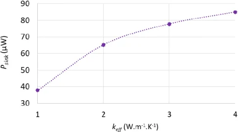
Figure 2.27: Power 𝑃𝑠𝑖𝑛𝑘 representing the tip-sample contact conductance for effective thermal conductivities 𝑘𝑒𝑓𝑓 between 1 and 4 W.m-1.K-1. ... 76
Figure 2.28: FEM modelling of the Wollaston probe in contact with a layer-on-substrate sample. .... 76
Figure 2.29: SThM measurements of the effective thermal conductivity for ULK and BD1 samples ... 77
Figure 2.30: Principle of the 3ω method. a) Top view of the four-probe electronic setup. b) Cross section of the heater which is the metallic line. ... 79
Figure 2.31: Cross section of the 3ω device on a real multilayer sample. ... 80
Figure 2.32: Influence of the surface layer on a bulk silicon sample on the temperature rise calculated following Borca-Tasciuc et al. ... 81
Figure 2.33: Fabrication steps for the deposition of the 3ω device in clean room... 82
Figure 2.34: Geometry of the heater for 3ω measurements. a) Top view of the heater geometry. b) Cross section of the metallic line. ... 82
Figure 2.35: Optical microscope images of the 3ω heater. a) Measurement of the length 𝐿 of the heater equal to 1.33 mm. b) Measurement of the width 2𝑏 of the wire equal to 11 µm ... 83
Figure 2.36: 3ω setup with a) helium Dewar to allow low temperature measurements, b) cryostat for measurements under vacuum and c) sample holder with wire bonding connections ... 83
Figure 2.37: Electrical resistance for SiCN 350, SiCN 600 and SiN 300 samples as a function of the temperature inside the cryostat. ... 84
Figure 2.38: Schematics of the electronic circuit for the measurement of the heater temperature oscillations 𝜃2𝜔 in the 3ω method. ... 85
Figure 2.39: Optical microscopy image of a 3ω heater with fabrication process problems. a) Inhomogeneity of metal density. b) Break of the metallic line. ... 85
Figure 2.40: Temperature rise 𝜃2𝜔/𝑃0 measured with 3ω method for USG, SiCN and SiN samples. .. 86
Figure 2.41: Measurement with the 3ω method for USG, SiCN and SiN samples. a) Intrinsic thermal conductivity. b) Thermal boundary conductance. ... 88
Figure 3.1: Schematic of the cross section of the test chip M3EM. ... 93
Figure 3.2: Design of the Metal Bottom level of M3EM. a) Heating elements with serpentine resistance. b) Geometry of the small right heater with an insert on a copper line. ... 94
Figure 3.3: Geometry of the copper dummies into the silicon dioxide matrix. a) Top view of the dummies. b) Cross section of one dummy. ... 94
Figure 3.4: Geometry of the hybrid bonding layer. a) Top view of the hybrid bonding pads. b) Cross section of one hybrid bonding pad. ... 95
Figure 3.5: Aspect ratio between the layer thicknesses and the setup dimension. ... 95
Figure 3.6: Representation of EMA with Maxwell-Garnett model... 96
Figure 3.7: Representation of EMA with Maxwell-Bruggeman model. ... 96
Figure 3.8: Representation of EMA with parallel and series thermal conductance. ... 97
Figure 3.9: Homogenization strategy for a multilayer structure like M3EM. ... 97
Figure 3.10: Homogenization of the in-plane thermal conductivity in metal levels. a) Geometry of the unit cell with the dummy. b) Calculation of the effective in-plane thermal conductivity. ... 98
Figure 3.11: a) Schematic of the BEOL cross section in ICs. b) Zoom on the periodic unit cell. ... 99
Figure 3.12: Homogenization of the cross-plane thermal conductivity in metal level. a) Geometry of the unit cell with the dummy. b) Calculation of the effective cross-plane thermal conductivity. ... 99
Figure 3.13: Geometry and boundary conditions considered for M3EM FEM model. ... 101
Figure 3.14: a) Wire bonding positions on the top die surface. b) Disc of heat transfer coefficient 𝑔𝑤𝑏 set as boundary condition with a pitch of 130 µm... 102
Figure 3.15: Measurement of the small right heater resistance as a function of temperature. ... 102
Figure 3.16: Heater average temperature as a function of the heat sink conductance. ... 103
Figure 3.17: Heater average temperature as a function of the heat loss coefficient. ... 103
Figure 3.18: Chip surface temperature rise calculated with homogenized BEOL. ... 104
Figure 3.19: a) Temperature rise at the center of the heater as a function of the depth. b) Insert on the temperature rise inside the BEOL and the top die. ... 104
Figure 3.20: Schematic of the heat flux distribution surrounding the BEOL. ... 105
Figure 3.21: a) Explicit geometry of the Metal Bottom layer for multiscale FEM modelling. b) Temperature rise of the small right heater in the Metal Bottom layer of M3EM. ... 106
Figure 3.22: Calculation of the up and down thermal conductance coefficients in FEM. ... 106
Figure 3.23: Temperature profile along the Y axis, at the middle of the heater. ... 107
Figure 3.24: Floorplan of the PCB for chip alimentation. a) PCB geometry. b) Pads characteristics. . 108
Figure 3.25: Schematic of the wire bonding between M3EM and the PCB. ... 108
Figure 3.26: Optical microscopy image of the wedge wire bonding realized at CIME Nanotech with a) aluminum pad on top die surface and b) copper pad on epoxy surface. ... 109
Figure 3.27: Power supply electrical circuit of the test chip M3EM. ... 109
Figure 3.28: Spectral radiance 𝐼 calculated with Planck’s law for a blackbody emission as a function of the temperature and the wavelength 𝜆. ... 110
Figure 3.29: Picture of the IR thermometer THEMOS-1000. ... 111
Figure 3.30: Principle of the emissivity calibration with IR thermometry. ... 112
Figure 3.31: a) M3EM emissivity measured with InSb camera. b) Profile along dashed line. ... 112
Figure 3.32: Temperature rise measured with IR thermometry on M3EM surface. ... 113
Figure 3.33: Thermometry coefficient determination by FEM modelling for a) palladium nano-probe and b) Wollaston micro-probe. ... 113
Figure 3.34: Variation of electrical resistance as a function of the injected Joule power for the Wollaston micro-probe for a) large electrical current and b) low electrical current. ... 114
Figure 3.35: Position of the points of measurements on the M3EM chip. ... 115
Figure 3.37: SThM surface temperature mapping with palladium and Wollaston probes. ... 116
Figure 3.38: Surface temperature rise for M3EM measured by SThM and IR thermometry. ... 117
Figure 3.39: Temperature rise calculated in FEM and measured with SThM and IR thermometry. .. 117
Figure 3.40: Effect of radiative heat transfer. Modelling by a TBC ℎ𝑟𝑎𝑑 and a heat sink 𝑃𝑟𝑎𝑑. ... 118
Figure 3.41: Schematic of M3EM cross section with a) location of the TBRs in the stack and b) equivalent FEM modelling with boundary conditions. ... 119
Figure 3.42: Influence of the TBR 𝑅𝑡ℎ on the temperature field calculated in FEM. ... 119
Figure 3.43: Influence of the EMA model on the temperature field calculated in FEM. ... 120
Figure 4.1: Schematic of the BEOL structure in the 3D hybrid bonding imager. ... 125
Figure 4.2: Characteristics of the different metal levels in the C40 bottom chip. ... 126
Figure 4.3: Schematic of the STI level in the C40 bottom. a) Cross section of the STI level in the 𝑧 direction. b) Floorplan of the STI in the 𝑥𝑦 plane. ... 127
Figure 4.4: Characteristics of the hybrid bonding level for the 3D BSI. ... 127
Figure 4.5: Schematic of the DTI level in the I140 top chip. a) Cross section of the DTI level in the 𝑧 direction. b) Floorplan of the DTI in the 𝑥𝑦 plane. ... 127
Figure 4.6: Characteristics of the different metal levels in the I140/I110 top chips. ... 128
Figure 4.7: Cross section of the pixel structure for I140 top chip. ... 129
Figure 4.8: Top view of the I140 pixel geometry for a) tungsten layer and b) resin micro lenses. ... 129
Figure 4.9: Surface characterization of the I140 imager in the 𝑥𝑦 plane. a) Optical microscopy image of the pixel array. b) AFM topography of the pixel micro lenses. ... 130
Figure 4.10: Positions of the embedded thermal structures in the FLAMINGO test chip. ... 130
Figure 4.11: TCR measurement for the M1 levels of C40 and I140 chips respectively. ... 131
Figure 4.12: Resistance measured as a function of the injected Joule power for: a) heater in the C40 bottom chip and b) sensor in the I140 top chip. ... 132
Figure 4.13: Temperature rise modeled by FEM for the homogenization of the M1X level with a) in-plane thermal and b) cross-plane conductivity homogenization. ... 132
Figure 4.14: Principle of the simplification for the FEM modelling of the pixel imager. a) Full layered geometry of the pixel. b) Homogenized equivalent level. ... 134
Figure 4.15: Cross section of the pixel stack without the micro lenses. ... 134
Figure 4.16: Heat flux distribution in the pixel stack along the directions 𝑥 and 𝑦. ... 135
Figure 4.17: Heat flux distribution in tungsten level along the direction 𝑧. ... 135
Figure 4.18: a) FEM model geometry of the pixel. Heat flux distribution in the pixel cross section with b) in-plane and c) cross-plane temperature differences. ... 136
Figure 4.19: Geometry and boundary conditions considered for FLAMINGO FEM model with a) PCB and 3D HB chip and b) BEOL layers and pixel thicknesses. ... 137
Figure 4.20: Optical microscopy image of the wedge wire bonding realized at CIME Nanotech with a) aluminum pad on top die surface and b) copper pad on epoxy surface. ... 137
Figure 4.21: Multi-scale FEM modelling of the pixel at the center of the die... 139
Figure 4.22: Temperature rise calculated by FEM with the FLAMINGO chip. a) Top surface in the 𝑥𝑦 plane. b) Along the 𝑧 axis in the BEOL at the center of the heater. ... 139
Figure 4.23: a) Temperature field and b) heat flux distribution in the 𝑥𝑧 plane calculated with multi-scale FEM approach in the pixel located at the center of the die. ... 140
Figure 4.24: Equivalence of heat dissipation ability between a heater on an edge and at the center of the chip when 𝑘𝑒𝑞 is equal to 𝑘𝑆𝑖/2 approximatly. ... 140
Figure 4.25: Heat dissipation as a function of the distance between the edge and the heater. a) Variable of the parametric study and b) temperature rise calculated on FLAMINGO chip. ... 141
Figure 4.26: Experimental setup for the SThM thermometry on FLAMINGO chip. a) Chip holder inside the MT-MDT SThM. b) Zoom on the chip holder geometry. ... 141
Figure 4.27: Power supply and electrical circuit of the 3D HB chip FLAMINGO. ... 142 Figure 4.28: Wheatstone bridge setup for SThM measurements. ... 143 Figure 4.29: a) Points array and scanning direction for mapping thermometry. b) Drift characterization as a function of the measurement time. ... 144 Figure 4.30: Thermometry mapping measurement. a) Raw data of voltage 𝑉𝑎𝑏. b) Filament and surface
temperature rise ∆𝑇𝑝 and ∆𝑇𝑠 taking into account the thermal drift 𝑉𝑑𝑟𝑖𝑓𝑡. ... 144
Figure 4.31: a) Points array and scanning direction for imaging thermometry. b) Drift characterization as a function of the point of reference. ... 145 Figure 4.32: Thermometry imaging measurement. a) Raw data of voltage 𝑉𝑎𝑏. b) Filament and surface
temperature rise ∆𝑇𝑝 and ∆𝑇𝑠 taking into account the thermal drift 𝑉𝑑𝑟𝑖𝑓𝑡. ... 145
Figure 4.33: FEM calculations as a function of ℎ𝑟𝑎𝑑 and SThM mapping measurement performed with
the Wollaston probe for center heater supply at the pixel matrix surface. ... 146 Figure 4.34: Comparison between FEM calculations and SThM imaging performed with the Wollaston probe for corner sensor supply in a) 𝑢 direction and b) 𝑣 direction... 146 Figure 4.35: Schematic of the 93D demonstrator. a) In-plane geometry of the chip with the wire bonding location. b) Cross-section of the chip and the ceramic package. ... 148 Figure 4.36: a) Location and b) geometry of the thermal structures in the C40 FEOL. ... 149 Figure 4.37: Heater power generation as a function of the voltage supply and the temperature. ... 150 Figure 4.38: Schematic of the PTAT sensor concept. ... 150 Figure 4.39: Schematic of the PTAT sensor temperature rise generated by the functional blocks (power supply, memory, signal treatment…), the heater elements and the heat gun. ... 151 Figure 4.40: Thermalization of the 93D demonstrator. a) Fit of the PTAT sensor temperature with exponential functions. Determination of the b) die and c) package time constants. ... 152 Figure 4.41: Dark current as a function of the temperature measured by the PTAT sensors. ... 153 Figure 4.42: Measurement with the pixel matrix of the 93D chip of a) the dark current intensity and b) the deduced surface temperature. ... 154 Figure 4.43: Transient behavior toward thermalization measured with the pixel matrix of the 93D chip at a frame rate of 30 Hz. ... 155 Figure 4.44: a) Geometry and boundary conditions applied on 93D chip FEM model. b) Boundary heat source generated by the thermal structure in the FEOL. ... 155 Figure 4.45: FEM modelling of the roughness effect on heat transfer through air. a) Geometry of the roughness (micro lens) and boundary conditions. b) Heat flux distribution in the 𝑦𝑧 plane. ... 156 Figure 4.46: Temperature profile from the measurements with the pixel matrix at steady state along the 𝑦 direction above the heater CENTER and comparison with the FEM modelling. ... 157 Figure 4.47: Transient temperature evolution calculated with FEM on the pixel array surface as a function of time after switching off the heater CENTER. ... 157 Figure 4.48: Transient temperature profile calculated with FEM on the pixel array surface along the 𝑦 direction after switching off the CENTER heater. ... 158 Figure 4.49: Temperature profiles calculated with FEM on the pixel array surface along the 𝑦 direction above the heater CENTER. Comparison between 𝑆𝑑𝑖𝑒 = 40 mm² and 𝑆𝑑𝑖𝑒 = 1 mm² at 𝑡 = 0. ... 158
Figure A.1: Pictorial explanation of a thermal boundary conductance. ... 167 Figure A.2: Phonon dispersion relation for bulk silicon. ... 168 Figure A.3: Calculation of a) group velocities and b) densities of states for both TA and LA phonon modes of propagation in silicon as a function of the circular frequency. ... 169 Figure A.4: Transmission coefficient between silicon and germanium calculated in AMM as a function of the incident angle and the circular frequency for each polarization. ... 170 Figure A.5: Transmission coefficient between silicon and germanium calculated in DMM as a function of the circular frequency. ... 171
List of Tables
Table 1.1: Advantages and drawbacks of the TSV and HB technologies. ... 34 Table 1.2: Advantages and drawbacks of the CCD and CMOS technologies. ... 37 Table 2.1: Characteristics of the different SOI samples used in this work. ... 58 Table 2.2: Characteristics of the different samples used in this work. ... 58 Table 2.3: Summary of material thermoresistive properties. ... 62 Table 2.4: Contact angle measurements and calculated water conductance per surface material. .... 64 Table 2.5: Values of interface conductance calculated with AMM and DMM theories. ... 65 Table 2.6: TBC calculated with AMM/DMM theories. ... 66 Table 2.7: Values of TBC calculated with AMM and DMM. ... 69 Table 2.8: Measurement of the thermal signal with the Wollaston probe on calibration samples. .... 71 Table 2.9: Comparison between palladium nano-probe and Wollaston capabilities. ... 77 Table 2.10: TCR 𝛼 and resistance 𝑅0 for SiCN 350, SiCN 600 and SiN 300 samples. ... 84
Table 2.11: Substrate thermal conductivity determined with 3ω method. ... 86 Table 2.12: Layer effective thermal conductivity determined with 3ω method. ... 87 Table 2.13: Intrinsic thermal conductivities and TBC for USG, SiCN and SiN materials. ... 87 Table 2.14: Capabilities of the 3ω method. ... 88 Table 2.15: Comparison between measurements (SThM with Wollaston probe and 3ω method) and literature for the effective thermal conductivity of USG, SiN, SiCN, BD1 and ULK thin films. ... 88 Table 2.16: Summary of the advantages and drawbacks for each characterization technique. ... 89 Table 3.1: Homogenization of in-plane and cross-plane thermal conductivities for the levels of M3EM with numerical and analytical procedures. ... 100 Table 3.2: Homogenized in-plane and cross-plane thermal conductivities for M3EM BEOL with numerical and analytical procedures. ... 100 Table 3.3: Summary of the heat flux distribution. ... 106 Table 3.4: Specifications of the three different IR lenses. ... 110 Table 3.5: Sensitivity to the injected current for both palladium and Wollaston probes. ... 115 Table 3.6: Summary of the heat flux distribution. ... 118 Table 3.7: Homogenized thermal conductivity for different EMA models. ... 120 Table 4.1: Properties of the thermal structures of FLAMINGO. ... 131 Table 4.2: Homogenized thermal conductivities for the levels of FLAMINGO test chip. ... 133 Table 4.3: Thermoresistive measurement of ∆𝑇 under vacuum conditions. ... 138 Table 4.4: Thermoresistive measurement of ∆𝑇 under ambient conditions. ... 138 Table 4.5: Summary of experimental conditions for the following study cases. ... 142 Table 4.6: Thermoresistive temperature rises measurement with FLAMINGO test chip. ... 147 Table 4.7: SThM temperature rises measurement on I140 pixel array surface. ... 147 Table 4.8: Heater temperature rise measured at steady state with PTAT sensor. ... 151 Table 4.9: Boundary conditions for 93D chip FEM modelling. ... 156 Table 4.10: Properties of the FLAMINGO and 93D chips. ... 159
Nomenclature
Abbreviation Term
AC Alternating Current
AFM Atomic Force Microscopy
AMM Acoustic Mismatch Model
BEOL Back-End-Of-Line
BL Bottom Left
BR Bottom Right
CCD Charge Coupled Device
CCM Conductivity Contrast Mode
CD Critical Dimension
CMOS Complementary Metal-Oxide-Semiconductor
CMP Chemical and Mechanical Planarization
DBI Direct Bond Interconnect
DC Direct Current
DMM Diffuse Mismatch Model
DTI Deep Trench Isolation
EMA Effective Medium Approximation
EUV Extreme Ultraviolet
FD Floating Diffusion
FE Finite Element
FEA Finite Element Analysis
FEM Finite Element Method
FEOL Front-End-Of-Line
FDM Finite Difference Method
FinFET Fin Field Effect Transistor
FWHM Full Width at Half Maximum
HB Hybrid Bonding
IC Integrated Circuit
IMG Imager
InSb Indium Antimonide
IR Infrared
LIA Lock-In Amplifier
LMC Lattice Monte Carlo
MC Monte Carlo
MD Molecular Dynamics
MEMS Microelectromechanical System
MOS Metal-Oxide-Semiconductor
MOSFET Metal-Oxide-Semiconductor Field Effect Transistor
NA Numerical Aperture
NMOS N-channel MOSFET
PCB Printed Circuit Board
PMOS P-channel MOSFET
PPD Pinned Photodiode
PTAT Proportional To Absolute Temperature
RF Radio-Frequency
RGB Red, Green, Blue
RH Relative Humidity
SEM Scanning Electron Microscopy
SoC System-on-Chip
SOI Silicon-On-Insulator
SNR Signal-to-Noise Ratio
SThM Scanning Thermal Microscopy
STI Shallow Trench Isolation
TBC Thermal Boundary Conductance
TBR Thermal Boundary Resistance
TCM Temperature Contrast Mode
TCR Temperature Coefficient of Resistance
TEC Thermal Expansion Coefficient
TG Transfer Gate
TIM Thermal Interface Material
TL Top Left
TR Top Right
TSV Through Silicon Via
TTI Thermoreflectance Thermal Imaging
ULK Ultra Low-k
USG Undoped Silicon Glass
UV Ultraviolet
WB Wire Bonding
1D One-Dimensional
2D Two-Dimensional
3D Three-Dimensional
Symbol Unit Description
𝑏 m Heater half-width 𝐷 m.s-2 Thermal diffusivity 𝐸 eV Energy 𝑓 s-1 Frequency 𝐺 W.K-1 Conductance 𝐺𝑐𝑜𝑛𝑡𝑎𝑐𝑡 W.K-1 Contact conductance
𝑔𝑠𝑖𝑛𝑘 W.m-2.K-1 Heat sink conductance
𝐺𝑤𝑎𝑡𝑒𝑟 W.K-1 Water meniscus conductance
𝑔𝑤𝑏 W.m-2.K-1 Wire bonding conductance
ℎ𝑎𝑖𝑟 W.m-2.K-1 Air losses coefficient
ℎ𝑟𝑎𝑑 W.m-2.K-1 Radiative losses coefficient
𝐼 A Current
𝐽 A.m-2 Current density
𝑘 W.m-1.K-1 Thermal conductivity
𝑘𝑏 m2.kg.s-2.K-1 Boltzmann constant
𝑘𝑒𝑓𝑓 W.m-1.K-1 Effective thermal conductivity
𝑃 W Power
𝑞 C Electron charge
𝑄 W.m-2 Heat flux density
𝑅 Ω Electrical resistance
𝑅𝑡ℎ K.m².W-1 Thermal resistance
𝑆 m² Surface
𝑇 K Temperature
𝑉 V Voltage
Greek letter Unit Description
𝛼 K-1 Temperature coefficient of resistance
∆𝑇 K Temperature difference
∆𝑅 Ω Electrical resistance difference
∆𝑉 V Voltage difference
𝜀 1 Emissivity
ħ J.s Normalized Planck constant
𝜆 m Wavelength
ꓥ m Mean free path
𝜔 rad.s-1 Angular frequency
𝜑 rad Phase
𝜙 W Heat flux
𝜎 W.m-2.K-4 Stefan-Boltzmann constant
Introduction
In this PhD thesis, self-heating phenomena are studied in 3D Integrated Circuit (IC) architectures. Here, we are interested more particularly in the 3D Hybrid Bonding (HB) technology for imagers in the context of their emergence in commercial devices. Indeed, in such architectures, the imager part (top chip) is located just above the control part (bottom chip), and the temperature of pixels is therefore expected to increase due to closeness with the heat sources. The pixel performance being strongly dependent on the temperature, the thermal behavior of 3D HB object needs to be perfectly understood and controlled to avoid performance drifts. In addition, the thermal stress associated to thermal gradients and local thermal expansion can also be detrimental to operation of the device. This is why it is important today to be able to determine a priori the thermal behavior of the associated ICs. Due to the specificity of a 3D object (versus a 2D one), the study focus on dedicated test chips and close-to-commercial devices of the current generation. Note that in contrast to many thermal studies, we are not investigating the hot spot (heat source) itself, but its impact on the temperature distribution and on the performance of components located further away.
In order to provide an accurate description of this problem, the thermal characteristics of the materials involved need first to be determined. At the submicron scale, numerous issues arise such as thermal properties characterization or thin film effects (interfacial resistance). This task, and those specificities intrinsically related to the microelectronic domain, will be also addressed in this work.
This report is made of four chapters and a conclusion section. Chapters 2-4 are the original contributions involving both entangled experimental and numerical tasks, while the first chapter provides an overview of key elements required for the understanding of the document. The contents of the chapters are detailed below.
In the first chapter, a state of the art of the influence of temperature on ICs is established in order to provide an overview of the specific issues in microelectronics. After having detailed the specificities of the recent imaging technologies, the thermal impact on various phenomenon such as electromigration, thermomechanical stress or dark current variation are presented. Hence, the performance of the chip, whether in terms of reliability or quality, is significantly impacted by the temperature. In the case of 3D HB imagers, this is all the more true for the optical performance of the pixel array.
Before investigating the thermal behavior of a 3D object, materials need first to be characterized. This work is described in the second chapter. Various dielectric thin films involving oxides, nitrides, and low-k compounds are evaluated. These materials and samples are chosen because they are the main components of the structure of an electronic chip for both the Front-End-Of-Line (FEOL) and the Back-End-Of-Line (BEOL). In order to characterize the thermal properties of our materials, two different electrothermal methods are implemented: Scanning Thermal Microscopy (SThM) and the 3ω method. SThM is a contact probe technique that allows to obtain a thermal signal at sub-micrometric scale. It allows to measure thermal variables/parameters such as temperatures, thermal conductivities or phase transition temperature for example. In SThM, the interpretation of the experimental data remains challenging. In order to allow quantitative data analysis, the heat transfer mechanisms between the probe and the sample are modelled by means of FE method involving heuristic parameters determined on physical basis. SThM measurements are performed with two types of probes: the palladium nano-probe and the Wollaston micro-probe. Concerning the 3ω method, it is a four-probe electrothermal method designed to measure the thermal conductivity of bulk materials
and thin films. 3ω devices are patterned by a photolithography process in clean room on top of the samples and heated with an alternating current. The effective thermal conductivity of the sample is deduced from the temperature rise of the wire. All the dielectric materials are investigated with these two techniques. The pros and cons of each method will be compared and discussed.
Chapter 3 aims to develop and validate a relevant approach of numerical modelling by FE for the prediction of the thermal behavior of 3D HB chips. A specific test chip used for the investigation of thermal issues, called M3EM, is detailed. The M3EM chip has been co-developed by ST Microelectronics and CEA LETI in order to quantify the efficiency of the HB fabrication process in terms of heat management. Embedded heaters and sensors (copper serpentines) located in the BEOL generate heat by Joule effect across the stack in order to represent the power generation of the functional blocks (i.e. power supply, memory signal treatment …) in real chips. In order to apply the FE method to the M3EM chip, a numerical method involving homogenization and a multiscale approach is proposed to overcome the issue raised by the large aspect ratios inherent to microelectronics. This procedure is validated by comparing calculations and experimental measurements performed with SThM, resistive thermometry and infrared microscopy on the M3EM test chip. The advantages and drawbacks of each method are described.
In chapter 4, the focus is on the thermal behavior of the 3D HB imager technology. To do so, methods and approaches, validated in the previous chapter, are applied on two different electronic chips. The first one, called FLAMINGO, is an analog test chip with an inactive pixel matrix and embedded electrothermal test structures. This chip was designed to validate the whole process and assembly flow in terms of mechanical reliability. The second chip, called 93D, is a demonstrator with an active pixel matrix. Both chips were therefore designed for different objectives and, thus, have different added value in the frame of this work. In a first step, the FEOL and BEOL structures of these two chips are detailed. In a second step, the FLAMINGO chip is used to study the thermal behavior of the pixel. SThM measurements are implemented to validate the numerical analysis at the pixel array level. In a third step, the optical performances with regard to the temperature field are evaluated thanks to the 93D demonstrator by means of PTAT sensors and pixel dark current performance. This allows experimental quantification of self-heating phenomena in true devices in terms of optical performances for different use cases, both in the static and dynamic regimes.
Finally, the main conclusions of this work are summarized in the last section. Some observations useful for the next generation of devices and the future method development are highlighted.
Chapter 1. 3D Hybrid Bonding imagers: context and
challenges
This chapter aims to provide the main ideas regarding 3D Hybrid Bonding (HB) imagers (IMG) and the thermal challenges related to this new technology. It therefore provides key ingredients for the following of the manuscript, however it does not address in depth all aspects, which can be found elsewhere with an improved level of detail (references are given). More precisely, here the technology is first detailed from a functional and manufacturing point of view. The 3D integration, the hybrid bonding and the pinned photodiode principle are explained in short. In a second step, an inventory of some key thermal constraints induced by the new technology is drawn, involving in particular thermomechanical stress, dark current generation and electromigration. Finally, different numerical and experimental methods for the characterization of heating and its impact on devices are briefly presented. Among all the methods available in the literature, some will be retained for use in this PhD work and applied in the following chapters.
I.
3D hybrid bonding technologies
In this section, the 3D HB IMG technology is detailed in three parts. First, a general description of the integrated circuit technology is provided. Then, the principle of 3D integration and the hybrid bonding technology are explained. Finally, the imaging technology architecture, embedded in the 3D stack, is detailed.
I.1.
Integrated circuits
Here, some very fundamentals about integrated circuits (IC) structure are recalled. Considering only the chip, an IC can be divided in two parts: the Front-End-Of-Line (FEOL) and the Back-End-Of-Line (BEOL).
I.1.A. General trends in microelectronics
Figure 1.1: Wafer diameter increase during the last decades [7].
In electronics, the substrate (called also “wafer”) [1] is a thin slice of semiconductor, e.g. silicon, germanium or gallium arsenide, depending on the technology. The bulk silicon wafer is the oldest technology but remains a staple of the microelectronic industry: it is used in many microelectronic
technologies. Its thickness is typically about 0.7 mm. Si wafers are usually made of single-crystal silicon fabricated with the Czochralski process [2]. During the last few years, the development of microelectronics has seen the emergence of a new type of wafer: the Silicon-On-Insulator (SOI) substrate [3]. The SOI technology refers to the use of a layered silicon-insulator-silicon substrate in place of conventional silicon substrate. This allows among other advantages to reduce parasitic capacitance in transistors and therefore increase electrical performance [4]. The choice of the insulator depends on the application. In the majority of cases, sapphire and silicon dioxide are used for high-performance radio frequency (RF) and microelectronics devices, respectively [5]. More generally speaking, the constant evolution of the Metal-Oxide-Semiconductor (MOS) technology has been driven during the last four decades by Moore and More than Moore’s law which assess that the density of components roughly double every two years [6]. In addition to improving substrate technologies, the microelectronic industry has continually sought to increase the diameter of wafers, which allows them to consistently reduce the manufacturing cost per transistor. A schematic of the wafer size increases in the last decades is shown in Figure 1.1 [7].
I.1.B. Front-End-Of-Line
In this section, the principle of the Front-End-Of-Line (FEOL) is explained at both MOS Field-Effect Transistor (FET) and die levels.
I.1.B.a. MOSFET principle
Figure 1.2: Schematic of the PMOS and NMOS of the CMOS40 technology.
The Front-End-Of-Line (FEOL) is the first portion of IC fabrication where the individual transistors are patterned in the semiconductor. The technologies used in this thesis are based on MOSFET (Metal-Oxide-Semiconductor Field-Effect Transistor). The MOSFET technology is used in both digital logic and analog circuits such as microcontrollers, memory and CMOS sensors for example [8]. The principle of the MOSFET is detailed in Figure 1.2. The electrical current flowing from the source to the drain is controlled electrically by the voltage applied on the gate. In the case of the n-doped CMOS transistor (NMOS), powering the gate generates an electron channel in the substrate. Conversely, without powering the gate, the transistor is like an open circuit. In the case of the PMOS transistor, the principle is the same with a channel of holes. Note that a technology name (i.e. CMOS40 in this thesis) refers to the gate length in nanometers.
I.1.B.b. FEOL processing
FEOL processing refers to the formation of the transistors directly in the silicon substrate. The FEOL surface engineering consists in different consecutive steps:
(i) growing the gate dielectric (usually silicon dioxide) with dry oxidation. The dry oxidation is usually used to form thin oxides in a device structure because of its good Si-SiO2interface
(ii) patterning the sources and drain regions with the photolithography process. This procedure combines several steps in sequence: cleaning, preparation, photoresist application, exposure and developing, etching and photoresist removal [10];
(iii) ionic implantation [11] and diffusion [12] of the dopants to obtain the desired electrical field in the MOSFET channel.
Considering that the length of the gate is directly related to the transistor density in the substrate, manufacturing techniques have been constantly improved to reduce the dimension of the gate. Lithography has been one of the key drivers for the semiconductor industry. Roughly half of the density improvements have been derived from improvement in lithography [13]. Indeed, the minimum feature size (critical dimension) 𝐶𝐷 is equal to:
𝐶𝐷 =𝑘1
𝑛 𝜆
𝑁𝐴, (1.1)
where 𝜆 is the wavelength of light used, 𝑁𝐴 (~1) is the numerical aperture of the lens, 𝑛 is the index of refraction and 𝑘1 (~0.4) is a coefficient that encapsulates process-related factors. Modern processes
use UV light (𝜆 = 193 nm from an Argon-Fluoride laser), which makes it possible to pattern details of the order of 80 nm [14, 15]. To get down to 50 nm, the last lens and silicon are immersed in ultra-pure water. Water having a refractive index equal to 1.44, the wavelength of the light that propagates there is divided by all, which improves the resolution by 30 to 40%. The next generation of lithography will use extreme ultraviolet (EUV), at around 13 nm leading ideally to critical dimensions of the order of a few nanometers. However, the limit of lithography seems to be reached because the use of X-rays is not possible due to physical constraints [16]. Nowadays, the latest technologies released in the market are below 22 nm (Intel, TSMC…).
I.1.C. Back-End-Of-Line
The Back-End-Of-Line (BEOL) is the second level of an ICs fabrication where the transistors are interconnected together via metal wires on several levels. A schematic of the BEOL is detailed in Figure 1.3. The BEOL structure includes:
(i) tungsten contacts (on transistor source, drain and gate). Tungsten is chosen because it is less sensitive to electromigration. This is in particular very important for the finest lines where the current density can be as high as 106 A.cm-2 [17, 18];
(ii) insulating layers (dielectrics). These layers need low-k dielectric constant in order to avoid parasitic RC coupling between the metal layers [19, 20];
(iii) barriers (silicon nitride, silicon carbo-nitride…) which avoid the diffusion of the copper atoms of the metallic levels in the layers of oxide [21];
(iv) metal levels and vias. In the case of recent technologies, copper is used for the metal levels of the BEOL due to its low electrical resistivity [22];
(v) a capping layer made of silicon nitride preventing contamination and humidity to enter into the BEOL [23];
(vi) bonding sites for chip-to-package connections (wire bonding, bumps…) with aluminum contacts [24].
In BEOL part of fabrication stage contacts (pads), interconnect wires, vias and dielectric structures are formed (see Figure 1.3). For modern IC process, up to 10 metal layers can be stacked in the BEOL.
Figure 1.3: Cross section schematic of the BEOL structure (not to scale).
I.2.
3D integration for ICs
In this section, the 3D Hybrid Bonding technology is detailed. First, the principle of 3D integration is explained. Then, two different 3D integration technologies are detailed: Through Silicon Via (TSV) and Hybrid Bonding (HB).
I.2.A. 3D integration principle
Figure 1.4: 3D stacking principle for heterogeneous integration.
Technological limitations induced by transistors size reduction having been reached, the development of 3D integration has therefore emerged. The principle of 3D integration is explained in Figure 1.4. Different functional devices (sensor, MEMS, power management, memory…) are stacked together in the vertical direction. 3D integration is also called “heterogeneous integration” [25, 26].
3D integration is particularly interesting for imaging applications. Indeed, in the conventional approach, the logic elements are located at the periphery of the pixel matrix (2D floorplan). Large die size, poor time constant and similar technology for both imager and digital components are the main drawbacks of such integration. All these limitations are resolved by means of the 3D integration: digital blocks are located below the pixel matrix, the signal treatment is improved and advanced digital technology can be used.
I.2.B. 3D integration technologies
The two most common technologies for 3D integration are presented here: the Through Silicon Via (TSV) and the Hybrid Bonding (HB) technologies. The advantages and drawbacks of these two technologies are compared.
I.2.B.a. Through Silicon Via
Figure 1.5: Schematic of TSV structure with a) via-first, b) via-middle and c) via-last.
A Through Silicon Via (TSV) is a vertical electrical connection that crosses completely a silicon die [27]. A schematic of TSV structures is shown in Figure 1.5. TSVs have some advantages for the semiconductor industry dealing with 3D integration: power, area and time are better compared with conventional interconnects such as wire bonding, ball bonding… [28]. Such integration uses similar process steps to the BEOL stack. Three different types of TSVs exist:
(i) via-first TSVs fabricated before FEOL manufacturing;
(ii) via-middle TSVs fabricated between FEOL and BEOL manufacturing; (iii) via-last TSVs fabricated after BEOL manufacturing.
I.2.B.b. Hybrid Bonding
Figure 1.6: Cross section schematic of the 3D Hybrid Bonding integration.
In the context of heterogeneous integration, another technology has become unavoidable in recent years: Hybrid Bonding (HB) [29]. The principle of HB is detailed in Figure 1.6. It is a permanent bond performed at the wafer scale that combines a dielectric bond with embedded metal to form interconnections. It has become known in the industry as Direct Bond Interconnect (DBI). HB can offer
high via density, good alignment and high bonding strength with stress-free hermetic-sealed bonding structure [30]. In addition, various low-temperature HB techniques allow saving thermal budget as much as possible [31]. Contrary to TSV integration, this one requires the development of new steps in the process flow as shown in Figure 1.7. Further details and challenges related to this specific process can be found in [32] for example.
Figure 1.7: Schematic of the Hybrid Bonding process flow [32]. I.2.B.c. Comparison between TSV and HB
Some advantages and drawbacks of the TSV and HB technologies are summarized in Table 1.1. Hybrid bonding giving many advantages [33-37], this technology has quickly expanded.
TSV HB
Advantages Process reliability
Cost fabrication
Low thermal budget High bonding energies Wafer/die-wafer bonding Thin pitch (< 15 µm) Low RC delay Drawbacks Electromigration Thermomechanical stress
High thermal budget
Surface preparation Thermomechanical stress
Table 1.1: Advantages and drawbacks of the TSV and HB technologies [33-37].
I.3.
Imaging technology
The current PhD thesis is especially concerned with devices for imaging. The two most common technologies for imaging are presented below: the Complementary Metal Oxide Semiconductor (CMOS) and the Charge Coupled Device (CCD) technologies. The advantages and drawbacks of these two technologies are compared.
I.3.A. CMOS image sensor
The principle of the photodiode, which is the fundamental brick of CMOS image sensors, is described first. Then, the architecture of the CMOS image sensor technology is detailed.
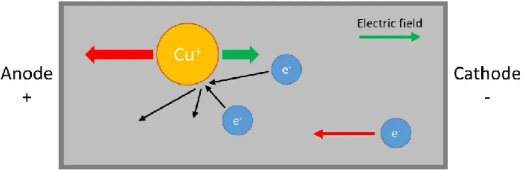
I.3.A.a. Pinned photodiode
A pinned photodiode (PPD) is a PN junction or PIN structure. When a photon of sufficient energy hits the diode, an electron-hole pair is created. This mechanism is also called photoelectric effect (see simplified schematic in Figure 1.8).
Figure 1.8: Principle of the photoelectric effect [38].
If the photon is absorbed in the junction’s depletion region, or up to one diffusion length away from it, the electron-hole pair is separated by the electric field of the depletion region. The hole moves toward the anode and the electron moves toward the cathode. A photocurrent is produced. The principle of the PN junction of the photodiode is explained in Figure 1.9. To first order, for a given spectral distribution, the photocurrent is proportional to the irradiance [39]. The photodiode can be used in two different modes:
(i) the photovoltaic mode is defined under zero bias. The photocurrent flows out of the anode through a short circuit to the cathode. This mode exploits the photovoltaic effect, which is the basis for solar cells;
(ii) the photoconductive mode when used in reversed bias. The response time is reduced because the additional reverse bias increases the width of the depletion layer, which increases the region with an electric field that will collect electrons quickly.
Figure 1.9: Depletion region at the PN junction of the photodiode following [40]. I.3.A.b. Pinned photodiode embedded in CMOS image sensor
A schematic of the PPD pixel is shown in Figure 1.10. The PPD is associated with a Transfer Gate (TG), which isolates the PPD from the Floating Diffusion (FD) during light integration (𝑉𝑇𝐺 off) and enables
electron transfer from the PPD to the FD for the readout of the output charge (𝑉𝑇𝐺 on). The Shallow
Figure 1.10: Structure of a PPD CMOS pixel for p-doped silicon [41]. I.3.B. CCD image sensor
Figure 1.11: Structure of a CCD pixel for p-doped silicon [42].
The CCD image sensor technology is based on the Metal Oxide Semiconductor (MOS) capacitor as shown in Figure 1.11. If a photon, with a sufficient energy, is absorbed in the depletion zone, an electron-hole pair is created. The electron remains in the depletion zone while the hole moves toward the substrate. The amount of negative charge (electrons) that can be collected is proportional to the applied voltage, the oxide thickness and the surface area of the gate. The total number of electrons that can be stored is called “well capacity”. When the wavelength increases, photons are absorbed at increasing depths. This notably limits the response to high wavelengths. Currently, available sensors can function from far infrared to X-rays.
I.3.C. Comparison between CCD and CMOS imagers
Key advantages and drawbacks of the CCD and CMOS image sensors are summarized in Table 1.2. Another design has been developed: the hybrid CCD/CMOS architecture consisting of CMOS readout integrated circuits that are bump bonded to a CCD imaging substrate has emerged. This technology has been adapted to silicon-based detector technology to mix the benefits of both CCD and CMOS imagers [44].
![Figure 1.19: Gap between chip power generation and TIM thermal conductivity [59], from a historical perspective](https://thumb-eu.123doks.com/thumbv2/123doknet/14501109.719240/43.892.258.631.851.1102/figure-gap-power-generation-thermal-conductivity-historical-perspective.webp)
![Figure 26: a) SEM image of SiN pattern. b) SThM thermal map of SiN pattern [81].](https://thumb-eu.123doks.com/thumbv2/123doknet/14501109.719240/48.892.202.689.184.438/figure-sem-image-sin-pattern-sthm-thermal-pattern.webp)
![Figure 1.31: FEM model for the calculation of mechanical stress in a TSV [93].](https://thumb-eu.123doks.com/thumbv2/123doknet/14501109.719240/51.892.206.695.549.776/figure-fem-model-calculation-mechanical-stress-tsv.webp)