HAL Id: hal-01779868
https://hal.archives-ouvertes.fr/hal-01779868
Submitted on 27 Apr 2018
HAL is a multi-disciplinary open access
archive for the deposit and dissemination of sci-entific research documents, whether they are pub-lished or not. The documents may come from teaching and research institutions in France or abroad, or from public or private research centers.
L’archive ouverte pluridisciplinaire HAL, est destinée au dépôt et à la diffusion de documents scientifiques de niveau recherche, publiés ou non, émanant des établissements d’enseignement et de recherche français ou étrangers, des laboratoires publics ou privés.
Design of a switch-mode power supply with soft
switching and analog control
E Baghaz, A Naamane, Nk M’Sirdi
To cite this version:
E Baghaz, A Naamane, Nk M’Sirdi. Design of a switch-mode power supply with soft switching and analog control. International Conference on Electronic Engineering and Renewable Energy (ICEERE’2018), Apr 2018, Oujda, Morocco. �hal-01779868�
Design of a switch-mode p
ow
er supply with soft switching and analog
control
E.Baghaz, A. Naamane, N.K M’sirdi
Aix Marseille Univ, Université de Toulon, CNRS, LIS, Marseille, France
Avenue escadrille Normandie Niemen 13397 Marseille cedex 20
Email : [email protected]
Abstract
In high-power applications to meet high-efficiency and green standards. Some power-supply designers have found it easier to use a D/DC, full-bridge converter. This is because this kind of converter can obtain zero-voltage switching on the primary side of the converter reducing switching losses, and EMI and increasing overall efficiency.
The purpose of this paper is the design of a switch mode power supply for industrial applications (vehicle battery charger, power supply for a helicopter…,).
This Full Bridge DC/DC converter controlled by an analog control. This shows several advantages as simple implementation, compactness with satisfactory performance. The simulation results obtained are compared with a Full Bridge Converter controlled by UCC28950 which is a digital Texas Instruments component. The designed power supply operates with an efficiency of more than 90%.
Keywords: Full Bridge DC/DC converter, analog control, UCC28950 controller, power supply, output
1
Introduction
In the field of power electronics, the choice of DC/DC converters depends the load specification of the desired application. Such as conventional DC/DC converters (Boost, Buck,...) are easy to implement, they require only one PWM signal to control the power switch. While, this type of converters are intended for limited current and voltage applications. Second, they suffer from a low-yield problem [1-4] because of the use of hard-switching controls, resulting in very significant output power loss during the switching of the transistor [1-4]. To address this problem, there are several structures of alternative power DC/DC converters for power applications [5,12]. In this context a new high power full bridge DC/DC converter is studied, with its analog controller. This proposed structure allows soft switching of the used transistors and as a result the overall efficiency is improved. The simulation results obtained are compared with those of converter controlled by a digital controller designed and produced by Texas Instruments.
2
Structure and operation of a Full Bridge DC/DC converter controlled by an analog
circuit
Figure 1 represents the synoptic diagram of the Full Bridge DC/DC converter, Figure 2, represents a full bridge phase DC/DC converter with its analog controller TA, TB, TC, and TD transistors form the complete bridge on the primary side of the T2 transformer, they switch with an appropriate cyclic ratio . TE, and TF represent the transistors on the secondary side of the T2 transformer. While LOut and VOut form the output filter. The Tr inductance is designed to assist the T2 transformer leakage inductance when operating in resonance with the internal capacity of the MOSFET and facilitates zero voltage switching (ZVT).
Figure1 Full bridge DC/DC
Figure 2. Control scheme of DC/DC converter
The analog control, it is based on the acquisition of the current generated by the input generator and the output voltage in order to generate 6 PWM synchronized signals to ensure the switching of the 4 Transistors (TA, TB, TC, TD) on the primary side of the transformer and those on the secondary side (TE, TF). As it is shown in the next figure A PI corrector is used
Figure 3 PI Corrector
The Acquisition of the current was carried out on the basis of the circuit shown in Figure 4, the transformer used for this application has a transformation ratio (m) of 100.
Figure 4 : current acquisition
V V U4 u A7 4 1 + 3 -2 V+ 7 V -4 O UT 6 O S1 1 O S2 5 V s1 C21 5 60 p IC = -1 R45 2 .37 k V BIA S3 D20 D1N5 40 6 0 C23 5 .6n IC = -1 R53 2 .37 k V pi V 1 0 V re f V BIA S2 R54 2 .37 k C24 1 u IC = 5 R55 9 .09 k R56 2 7.9 k V ou t D21 D1N5 40 6 D22 D1N5 40 6 I1 2 5u A dc V ssc C22 1 0n V BIA S1 0 0 CS Rcs D20DN4148 T 1 N = 100 R1 Vinput 410Vdc 0 DC/DC Converter
1 1 * 1 ( )* 6.88 * 2 *2* INMIN MAX L p MAG SW V D I Ps I A Vs m L F , 1 ( 0.3) 20.89 ( *1.1) p CS p V R I n
(1)
R7n R* CS 800
The PWM signal is obtained by the following circuit :
The PWM signal obtained above is connected with a flip flop JK toggle. The Q output of this toggle will only change the state if the PWM signal connected to its CLK input is in the rising front. The signal Q and Q ̅ at the output of the JK are two PWM signals (QC and QD) that will control a leg of the DC/DC converter Full Bridge. Then, a delay of 360ns is applied to the front amount of two signals Q and Q ̅, which ensures a switching to zero voltage (soft switching), avoiding the switching losses. The simulation results are shown in Figure 6, by connecting the PWM signal obtained to a JK flip flop, we obtain the signal from Figure 7 in green. One notices the JK has a rising edge behavior, for its state changes. The outputs Q and Q-, at the output of the JK flip flop, are shifted at each front up to 60ns. (Fig 6 F & G).
Fig.5. PWM signals connected to transistors TC et TD.
Fig 6, represents the complete circuit of the switching mode power supply, implanted in the Pspice simulator. We represent in the following the different simulation results obtained.
V s1 V ra m p P WM U5A L M3 1 9 O UT 1 2 + 4 -5 G 3 V + 1 1 V -6 V BIA S2 R49 4 .7k 0 I N1 O UT I N2 R64 1 k Cs1 C29 3 30 p 0 Cs 0 V 40 T D = 0 T F = 5u P W = 0 u P ER = 5 u V 1 = 0 T R = 5u V 2 = 0.6 5 V s2 U21 JKFF_ABM J CLK K Q Q PWM VBIAS U11 AND2 1 2 3 U12 AND2 1 2 3 QC QD U25 360ns DELAY U26 360ns DELAY Time
680us 685us 690us 695us 700us V(Startup.PWM) V(Startup.U11:I0) 0V 2.0V 4.0V 6.0V Time 4.715ms 4.725ms 4.735ms V(Startup.U11:I1) V(Startup:QC) 0V 1.0V 2.0V 3.0V 4.0V Time 4.715ms 4.725ms 4.735ms V(Startup.U21:Qbar) V(Startup:QD) 0V 1.0V 2.0V 3.0V
4.0V Fig. 6. Signals generated by the circuit in
Figure 5: E: PWM signal connected to the flip flop JK input (pink) and the one at its output (green); F: PWM signal QC (in red) of the JK flip flop (in green); G: QD PWM signal (in red). the output (Q) ̅ of the JK flip flop (in green).
E
F
Fig.6. Complete circuit of the Supply switch mode
4
. Performance comparison of the designed control and the UCC28950 controller
In order to show the performance of the analog control designed during this work, we compared the different signals of the Full Bridge converter , controlled by the designed control and the UCC28950 controller. The different results obtained are shown in Figure 7.It is to note that the results of the system controlled by the analog control designed are shown in Figure 7 on the left and those of system controlled by UCC28950 [11] are shown on the Same figure on the right. Based on the results obtained,
The comparison of the OUTA PWM signal generated by the two controls shows that they have the same cyclic ratio of 0.47, the same frequency of 100 kHz.
Fig.7. OUT A PWM signals,
Fig.8. Output transformer current generated
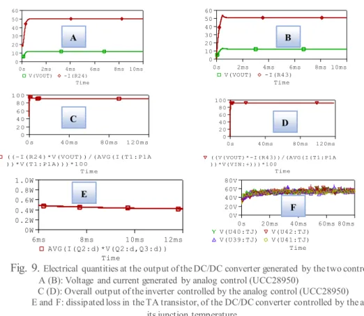
The electrical quantities at the output (voltage, current) generated by the analog control designed (Figure 9 A) are identical with those generated by the UCC28950 (Figure 9 B). The analog control designed in this work has a satisfactory performance, its efficiency is higher than 90% (figure 9C). It is identical to that generated by the UCC28950 controller (figure 9D).
So, the analog control designed during this work generates well-synchronized PWM signals, which ensures smooth transistors switching of the DC/DC converter. In order to clearly show these advantages,
0 0 0 C19 5n U37 C3D10065A A 1K 2 CASE3 C20 5n U38 C3D10065A A 1K 2 CASE3 L3 2uH L6 26uH I V V V V C15 5n C16 5n C17 5n C3_2 ESR = 0.01 X = 1 C = 330u IC = 400 C18 5n V1 410Vdc OUT C U39 C2M 0080120D D 1 G 2 S 3 T J 4 T C5 U40 C2M 0080120D D 1 G 2 S 3 T J4 T C5 U41 C2M 0080120D D 1 G 2 S 3 T J 4 T C5 U42 C2M 0080120D D 1 G 2 S 3 T J4 T C5 R52 240m CS VOUT V2 25Vdc V3 25Vdc V4 25Vdc V5 25Vdc 0 0 R1_2 8 0 0 0 U6 IR2111 1 1 22 3 3 U7 IR2111 1 1 22 3 3 0 0 OUT F D1DN4148 Q6 FDP032N08 Q5 FDP032N08 T 1 N = 100 R2_2 4.87k C14 125m D11 M URS360T 3 D5 M URS360T 3 OUT E OUT B OUT A VOUTP CS Startup Startup Cs Vout QC QD QA QB OUT C OUT D U43 RSFF SE 1 CLK 2 RE 3 Q4 Q5 U44 RSFF SE 1 CLK 2 RE 3 Q4 Q5 VBIAS2 VBIAS2 OUT A OUT C OUT B OUT D OUT F OUT E V37 5Vdc VBIAS2 0 U22 C3D10065A A 1K 2 CASE3 T 2 LLEAK = 7.5u NP1 = 21 RP1 = 0.215 LM = 2.6m NS1 = 1 RCORE = 100K RS1 = 0.58m NS2 = 1 RS2 = 0.58m U2 IR2111 1 1 22 3 3 U3 IR2111 1 1 22 3 3 U4 IR2111 1 1 22 3 3 U5 IR2111 1 1 22 3 3 U23 C3D10065A A 1K 2 CASE3 OUT A OUT B OUT D U24 C3D10065A A 1K 2 CASE3 U25 C3D10065A A 1K 2 CASE3 Time 5.00ms 5.01ms 5.02ms 5.03ms V(OUTA) V(OUTB) 0V 1.0V 2.0V 3.0V 4.0V Time 5.00ms 5.01ms 5.02ms 5.03ms V(OUTA) V(OUTB) 0V 4V 8V 12V 16V Time 5.00ms 5.01ms 5.02ms 5.03ms I(T2:S1A) 0A 10A 20A 30A 40A 50A 60A Time 5.00ms 5.01ms 5.02ms 5.03ms I(T2:S1A) 0A 10A 20A 30A 40A 50A 60A A B A B
we have shown in Figure 9 and F, the power losses and the junction temperature of the four transistors, of the Full Bridge DC/DC converter, during the transistor switching. It appears that, the power losses in each transistor is low, they do not exceed 0.5 W. Then the junction temperature of each transistor is about 50 °C. The results obtained clearly show the advantage of the control designed during this work.
Fig. 9. Electrical quantities at the output of the DC/DC converter generated by the two controls: A (B): Voltage and current generated by analog control (UCC28950)
C (D): Overall output of the inverter controlled by the analog control (UCC28950)
E and F: dissipated loss in the TA transistor, of the DC/DC converter controlled by the analog control,and its junction temperature.
5 Conclusion
In this paper, we have developed a power supply with a high current. It allows to generate a voltage of 12V current, a current of 50A, a power of 600W. It operates at a switching frequency of 100 kHz. This power supply is represented by a Full Bridge DC/DC converter controlled by an analog Control. Pspice provides an effective environment for modeling and simulation of this proposed DC/DC converters. The simulation results show the reasonability and validity of the control design.
As conclusion analog controller model gives very good dynamic respond compare with commercial digital controller model. It achieves our goal; it gives the same results as the commercial controller. Other advantages include smaller size and lighter weight (from the elimination of low frequency transformers which have a high weight) and lower heat generation due to higher efficiency.
References
1. E. Baghaz, M. Melhaoui, M. F. Yaden and K. Kassmi. Photovoltaic System Equipped with a DC/DC Buck Converter and a MPPT Command Ensuring an Optimal Functioning
2. http://vincent.boitier.free.fr/TER/809PET-boost-converter-efficiency-calculations.pdf
3. Elhadi BAGHAZ. Architectures discrétisées de gestion de l’énergie fournie par les systèmes photovoltaïques. Thèse soutenue à l’université Mohamed Premier d’Oujda, Juin 2015.
4. Cedric Cabal. Optimisation énergétique de l'étage d'adaptation électronique dédié à la conversion photovoltaïque. Thèse Délivrée par l’Université Toulouse III – Paul Sabatier, décembre 2008.
5. L. Balogh, “The current-doubler rectifier: An alternative rectification technique for push-pull and bridge converters,” Unitrode Integrated Circuit Corporation, Design note, DN-63, 2001, pp.1–5.
6. L. Balogh, “Design Review :100 W, 400 KHz DC-DC converter with current doubler synchronous rectification achieves 92% efficiency”. Texas Intrument, Design Review, 2001, pp.1–40.
Time 0s 2ms 4ms 6ms 8ms 10ms V(VOUT) -I(R24) 0 10 20 30 40 50 60 Time 0s 2ms 4ms 6ms 8ms 10ms V(VOUT) -I(R43) 0 10 20 30 40 50 60 Time 0s 40ms 80ms 120ms ((-I(R24)*V(VOUT))/(AVG(I(T1:P1A ))*V(T1:P1A)))*100 0 20 40 60 80 100 Time 0s 40ms 80ms 120ms ((V(VOUT)*-I(R43))/(AVG(I(T1:P1A ))*V(VIN:+)))*100 0 20 40 60 80 100 Time 6ms 8ms 10ms 12ms AVG(I(Q2:d)*V(Q2:d,Q3:d)) 0W 0.2W 0.4W 0.6W 0.8W 1.0W Time 0s 20ms 40ms 60ms 80ms V(U40:TJ) V(U42:TJ) V(U39:TJ) V(U41:TJ) 0V 20V 40V 60V 80V A B C D E F
7. Z. Sun, B. Eng, “Full bridge DC/DC converter with zero current switching synchronous rectification for auxiliary power units,”McMaster University, 2014.
8. X. Zhao, J.M. Guerrero, and X. Wu,’’Review of aircraft electric power systems and architectures,’’ in Proc. IEEE International Energy Conference (EnergyCon’14), 2014.
9. N. Kutkut, “A full bridge soft switched telecom power supply with a current doubler rectifier,” in Proc. Telecommunications Energy Conference, 1997. INTELEC 97., 19th International, Melbourne, Vic., 19–23 Oct 1997, pp.344–351
10. M. O’Loughlin, “UCC28950 600-W, phase-shifted, full-bridge application report,” TI Lit. No. SLUA560B, pp. 1–30, Sept. 2010.
11. http://www.ti.com/lit/ds/symlink/ucc28950.pdf
12. http://www.wolfspeed.com/media/downloads/161/C2M0025120D.pdf .