HAL Id: hal-02311382
https://hal.archives-ouvertes.fr/hal-02311382v2
Submitted on 14 Oct 2019
HAL is a multi-disciplinary open access
archive for the deposit and dissemination of sci-entific research documents, whether they are pub-lished or not. The documents may come from teaching and research institutions in France or abroad, or from public or private research centers.
L’archive ouverte pluridisciplinaire HAL, est destinée au dépôt et à la diffusion de documents scientifiques de niveau recherche, publiés ou non, émanant des établissements d’enseignement et de recherche français ou étrangers, des laboratoires publics ou privés.
Memristor Device Characterization by Scanning
Microwave Microscopy
G. Sassine, N. Najjari, C Brillard, N. Defrance, O Haenssler, Didier Theron,
F. Alibart, K. Haddadi
To cite this version:
G. Sassine, N. Najjari, C Brillard, N. Defrance, O Haenssler, et al.. Memristor Device Characterization by Scanning Microwave Microscopy. International Conference on Manipulation, Automation and Robotics at Small Scales (MARSS), Jul 2017, Montréal, Canada. �10.1109/MARSS.2017.8016537�. �hal-02311382v2�
Memristor Device Characterization
by Scanning Microwave Microscopy
1G. Sassine, 1N. Najjari, 1C. Brillard, 1N. Defrance, 1,2O. C. Haenssler , 1D. Theron, 1F. Alibart and 1K. Haddadi
1Institute of Electronics, Microelectronics and Nanotechnology (IEMN), University of Lille, CNRS, UMR 8520
Avenue Poincaré CS 60069 – 59652 Villeneuve d’Ascq Cedex – France
2 Department for Computing Science, University of Oldenburg, 26129 Oldenburg, Germany.
Abstract— We report memristive device characterization using
near-field scanning microwave microscopy. Atomic force microscopy, magnitude and phase-shift images of the complex reflection coefficient of TiO2 devices can be acquired
simultaneously in the range 1-20 GHz. In particular, measurement of the complex reflection coefficient of a 200 by 200 nm2 TiO
2 device is exemplary demonstrated. These
results are beneficial for electrical modeling and optimization of memristor devices to address OxRAM applications.
Keywords—Oxide based random access memory (OxRAM),
memristor, scanning microwave microscopy, atomic force microscopy, interferometry, metal oxide semiconductor capacitors.
I. INTRODUCTION
Resistive random access memory (RRAM) technologies have experienced an increasing interest these last years as a promising solution for storage and memory [1]. Indeed, emerging memory devices can offer potential alternative for flash technology or DRAM, thanks to their fast switching performances, high retention and cycling endurance, scalability, and back-end-of-line integration potential. Global understanding of the relative contribution of the different physical mechanisms is very challenging and significant efforts at the modeling and material characterization levels are still needed [2].
In this paper, we propose an analysis in the microwave domain to study dynamics in nanometer memristive devices. In particular, we consider TiO2 material that has been largely
investigated as prototypical material system for switching. A broadband near-field scanning microwave microscope (NSMM) consisting of an atomic force microscope combined with a vector network analyzer (VNA) is used to study the memristive devices [3]. Basically, the tip scans across the sample, emitting a microwave signal scattered by the material, altering its amplitude or/and phase properties [4-9]. The measurement set-up and device fabrication including dedicated calibration kit are described in Section II. Preliminary experimental results are presented in Section III. In particular, microwave response of the memristive device as a function of the applied bias is demonstrated around 18 GHz.
II. MATERIAL AND METHODS
A. Interferometric SMM setup
The interferometric set-up of the NSMM is depicted in Fig. 1. It consists of a KeysightTM LS5600 AFM interfaced
with a KeysightTM PNA series network analyzer E8362B
through a homemade tuned interferometric matching network based on the Mach-Zehnder method [10-11]. This latter is built up in coaxial form with a power divider, two hybrid couplers, an active variable attenuator and two amplifiers in series. The basic principle consists in splitting the PNA source high frequency power wave a1 in two coherent signals, i.e. the
reference signal aINC to the AFM tip and the interference
signal. The coupler associated to the AFM tip acts as a reflectometer to separate the incident wave aINC and the
reflected wave aREF from the device under test (DUT). The
wave aREF is then combined with the interference signal to
provide the output signal a3 at the output of the second
coupler. This signal a3 is cancelled by properly tuning the
attenuator to balance the magnitudes of aREF and the
interference signal. The resulting signal a3 signal is amplified
and measured by the PNA receiver.
Fig. 1. Set-up of the scanning microwave microscope incorporating a tuned interferometric matching network based on the Mach-Zehnder method.
The resulting measured reflection coefficient Γ = 𝑎$⁄ 𝑎% considering ideal components can be expressed as a function of the reflection coefficient Γ'()= 𝑎*+,⁄𝑎-./ of the DUT by:
Γ = 𝛼(Γ'()+ 𝛽) (1)
where 𝛼 is a complex coefficient taken into account losses and phase-shifts introduced by the microwave circuitry and 𝛽 denotes the interference signal. At the test frequency and for a DUT with reference impedance ZREF, the magnitude of the
reflection coefficient Γ is set to zero resulting in high measurement sensitivity for impedances around ZREF.
B. OxRAM devices and calibration kit fabrication
TiO2 devices were realized on a P-type silicon substrate of
resistivity 1–3 Ωcm (Fig. 2). The devices consist of Ti (5 nm)/Pt (30 nm)/TiO2-x/TiO2/Pt (15 nm)/Au (20 nm) from
bottom to top. All metals were deposited by e-beam evaporation, and top electrodes were patterned by electron beam lithography (EBL) with targeted dimensions between 200´200 and 60´60 nm2. TiO2-x/TiO2 films were obtained by
atomic layer deposition (ALD) at 200°C with TiCl4 as Ti
precursor and H2O as oxygen source. The water pulses were set
shorter than the ones needed to saturate the surface in order to produce an oxygen deficient TiO2-x layer. Post-deposition
oxidation of the TiO2-x top interface into TiO2 was obtained by
natural air exposure.
Fig. 2. Configuration of TiO2 devices under the AFM probe.
An on-wafer calibration kit consisting of MOS capacitors was fabricated on the same wafer. The MOS capacitors are composed of circular gold electrodes evaporated on SiO2
deposited on one part of the wafer (Fig. 3). In order to vary the capacitances values, the diameter of the upper gold pad varies from 0.5 to 2 μm whereas the SiO2 thickness was set to
140 nm.
From the AFM image, the topography of the TiO2 devices are
extracted along the wafer (Fig. 4). The data indicate a good homogeneity of the fabrication process.
Fig. 3. AFM topography image of the fabricated sample. On the left, MOS capacitor top electrodes are measured. On the right, the OxRAM stacks are measured.
Fig. 4. 1D topography cross section of the fabricated TiO2 devices
from top to bottom of the Fig. 2 image. The size of the OxRAM devices vary from 200´200 down to 60´60 nm2.
The impedance of the MOS structures measured at the tip apex of the probe is modeled by a series model consisting of an oxide capacitance 𝐶ox and a depletion capacitance 𝐶depl. Both capacitances can be described by the parallel plate capacitor formalism. The resulting capacitance 𝐶TOT is given by
𝐶TOT= 𝐶ox𝐶depl⁄8𝐶ox+𝐶depl9. (2) The parallel-plate capacitance term 𝐶ox without taking into account the fringing fields is calculated from the area A of the gold pads and the SiO2 thickness dox:
Cox =A ε<εrSi02
>ox . (3)
The silicon dioxide is assumed to have a relative dielectric constant of εrSi02 = 3.9. The thickness and areas of the capacitors were estimated from the AFM topography measurements (Fig. 3) to take into account any deviation in geometry induced by the fabrication process of the calibration kit. The measured areas A were 1.13 μm2, 3.94 μm2 and 13.85 μm2. The charge
stored on the capacitor is distributed across a certain depth that adds the depletion series capacitance 𝐶depl in series to 𝐶ox. The capacitance was estimated to be proportional to the area A of the metallic electrode and inversely proportional to the depleted zone depth ddepl according to
𝐶>?@A= 𝐴C><CDEF
GHIJ, (4)
with 𝑑>?@A= L2𝜀O𝜀PQRΨ 𝑞𝑁⁄ V and 𝜀PQR = 12 is the relative permittivity of the silicon bulk substrate, Ψ represents the energy band bending at the Si/SiO2 interface and is set to 200
mV, q is the elementary electron charge (1.6´10-19 C), 𝑁
V is the doping level of the silicon bulk around 8´1015 cm-3. From
relations (2) to (4), theoretical capacitance data can be derived. III. EXPERIMENTAL RESULTS
The measurements were performed in contact mode around 18 GHz using a 25PT300A AFM tip from Rocky Mountain NanotechnologyTM. The RF power source is set to -30 dBm
and the intermediate frequency bandwidth (IFBW) of the VNA is 100 Hz. The images were scanned over a 20´20 μm2 with
2048 pixels. In addition to the topography image, the NSMM provides both magnitude and phase-shift images of Γ. Fig. 5 shows the image of the magnitude of the reflection coefficient obtained under zero-bias conditions at f ~ 17.89 GHz.
Fig. 5. Image of the magnitude of the reflection coefficient Γ at f ~ 17.89 GHz.
The measurement reliability is influenced by the quality of the electrical contact between tip and sample especially for capacitance gold pads. We observe on some pixels a loss of the contact between the probe and the sample during the scanning. The loss of electrical contact is most likely caused by transient contamination of the gold pads. 200Í200 nm2 OxRam devices
(upper right of the image) are measured with high sensitivity. Magnitude contrast in respect with the background is between 18 and 24 dB. Smallest devices are also very sensitive to the microwave signal but exhibit different responses for devices of same size. A similar phenomenon is observed for the phase-shift of Γ.
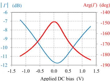
Fig. 6 shows the variation of the magnitude and phase of Γ as a function of the DC bias applied between probe tip and the bottom of a 200´200 nm2 device.
Fig. 6. Measured magnitude and phase of Γ as a function of the DC bias at f ~ 17.89 GHz.
From these data, variations of respectively 5 dB and 30 degrees are observed on the measured data when the DC bias is changed from -1.2 to 1.2 V. This is related to the dependence of the device impedance under DC bias.
IV. CONCLUSION
Near-field scanning microwave microscopy measurement of memristive devices have been experimentally demonstrated around 18 GHz. In particular, DC bias voltage impacts both magnitude and phase-shift responses of the microwave reflection coefficient in a sensitive manner. These preliminary results are instructive for further electrical modeling of the device. In particular, future works will include full vector calibration of the devices in a broad frequency range.
ACKNOWLEDGMENT
This work is supported by the French National Research Agency (ANR) and German Research Foundation (DFG) – project VACSMM. This work used the support of the RENATECH-IEMN for device fabrication. This work used the facilities within the EQPX ExCELSiOR.
REFERENCES
[1] A. C. Torrezan, J. P. Strachan, G. Medeiros-Ribeiro and R. S. williams; “Sub-nanosecond switching of a tantalum oxide memristor”, Nanotechnology”, vol. 22, no 48, p. 485203, 2001.
[2] G. Sassine, S. La Barbera, N. Najjari, M. Minvielle, C. Dubourdieu and F. Alibart, “Interfacial versus filamentary resistive switching in TiO2 and
HfO2 devices”, J. of Vacuum Science & Technology B, Nanotechnology and Microelectronics: Materials, Processing, Measurement, and Phenomena, vol. 34, no 1, p. 012202, 2016.
[3] S. M. Anlage, V. V. Talanov, and A. R. Schwartz, “Principles of near-field microwave microscopy,” Scanning Probe Microscopy: Electrical
and Electromechanical Phenomena at the Nanoscale, S. Kalinin and A. Gruverman, Eds. New York, Springer Sci., pp. 215–253, Aug. 2007.
Applied DC bias (V) │Γ│ (dB) Arg(Γ) (deg) -190 -180 -170 -160 -150 -140 -12 -11 -10 -9 -8 -7 -6 -1.5 -1.0 -0.5 0.0 0.5 1.0 1.5
[4] S. Fabiani, D. Mencarelli, A. Di Donato, T. Monti, G. Venanzoni, A Morini, T. Rozzi, and M. Farina, “Broadband Scanning Microwave Microscopy investigation of graphene”, Proc. IEEE MTT-S International
Microw. Symp., pp. 1-4, June 2011.
[5] G. Gramse, M. Kasper, L. Fumagalli, G. Gomila, P. Hinterdorfer and F. Kienberger, “Calibrated complex impedance and permitivity measurements with SMM,” Nanotechnology, vol. 25, no. 14, p. 8, 2014. [6] Agilent Technologies, Inc., “Scanning Microwave Microscopy (SMM)
Mode”, Datasheet, 2013.
[7] Oxford Instruments, Inc., “Scanning Microwave Impedance Microscopy (sMIM)”, Datasheet, 2014.
[8] A. Imtiaz, T. M. Wallis and P. Kabos, "Near-Field Scanning Microwave Microscopy: An Emerging Research Tool for Nanoscale Metrology”,
IEEE Microwave Magazine, vol.15, no.1, pp.52-64, Jan. 2014.
[9] K. Haddadi, D. Glay and Tuami Lasri, A 60 GHz scanning near-field microscope with high spatial resolution sub-surface imaging, IEEE
Microw. Wirel. Compon. Lett., 21, no. 11, pp. 625-627, 2011.
[10] T. Dargent, K. Haddadi, T. Lasri, N. Clément, D. Ducatteau, B. Legrand, H. Tanbakuchi, and D. Théron, “An interferometric scanning microwave microscope and calibration method for sub-fF microwave measurements”, Rev. Sci. Instrum., vol. 84, no.12, pp. 123705-123705-7, Dec. 2013.
[11] H. Happy, K. Haddadi, D. Théron, T. Lasri and G. Dambrine, “Measurement techniques for RF nanoelectronic devices : new equipment to overcome the problems of impedance and scale mismatch”, IEEE