HAL Id: hal-03047713
https://hal.archives-ouvertes.fr/hal-03047713
Submitted on 8 Dec 2020HAL is a multi-disciplinary open access archive for the deposit and dissemination of sci-entific research documents, whether they are pub-lished or not. The documents may come from teaching and research institutions in France or abroad, or from public or private research centers.
L’archive ouverte pluridisciplinaire HAL, est destinée au dépôt et à la diffusion de documents scientifiques de niveau recherche, publiés ou non, émanant des établissements d’enseignement et de recherche français ou étrangers, des laboratoires publics ou privés.
Indium segregation mechanism and V-defects formation
on (0001) InAlN surface: an ab-initio investigation
Ranim Mohamad, Pierre Ruterana
To cite this version:
Ranim Mohamad, Pierre Ruterana. Indium segregation mechanism and V-defects formation on (0001) InAlN surface: an ab-initio investigation. Journal of Physics D: Applied Physics, IOP Publishing, 2020, 54 (1), �10.1088/1361-6463/abb621�. �hal-03047713�
1
Journal of Phys D: Applied Phys. Accepted Manuscript
Indium segregation mechanism and V-defects formation on (0001) InAlN
surface: an ab-initio investigation
Ranim Mohamad*
aand Pierre Ruterana
Centre de Recherche sur les Ions, les Matériaux et la Photonique UMR 6252, CNRS ENSICAEN UCBN CEA, 6 Boulevard du Maréchal Juin, 14050 Caen Cedex, France.
*
Author for correspondence : Ranim.Mohamad@cnrs-imn.fr
bPresent address : Institut des Matériaux Jean Rouxel (IMN)-UMR6502, Université de Nantes, CNRS, 2 rue de la
Houssinière, BP 32229, 44322 Nantes Cedex 3, France
Abstract
First principle calculations were performed to investigate adsorption and diffusion of indium and aluminum atoms on (0001) and (0001̅) In (18%) AlN surfaces. First, it was shown that these surfaces are most stable when they contain complex defects. The presence of vacancies causes the In to be strongly bound to the surface with the adsorption energy increasing by 0.11 eV for metal-polar and by 0.78 eV N-polar. In contrast, the adsorption strength of Al to the surface with defects decreases; the corresponding energy goes from 3.96 eV to 2.29 eV (metal-polar) and from 8.30 eV to 5.05 eV (N-polar). Simultaneously, the diffusion of In is reinforced; its energy barrier decreases by 0.74 eV (0.06 eV) for N-polar (metal-polar) InAlN surface, whereas that of the Al adatom increases by 0.32 eV for metal-polar (0.08 eV for N-polar) which should limit its the diffusion on the surface. Therefore, the indium atoms will tend to migrate towards the complex defects. Eventually, during the epitaxial growth, this aggregation of indium atoms around the defects and the low mobility of Al atoms could be at the origin of the observed V defects, the phase separation and the crystallographic degradation of the InAlN epitaxial layers with increasing thickness.
2
I.
Introduction
For almost 20 years, InAlN has been attracting a large attention for use as attractive layer in optoelectronic and electronic devices: Bragg mirrors [1] and high electron mobility transistors (HEMT) [2], due to its lattice match with GaN for a composition of indium around 18% when grown along [0001] with a band gap around 4.2 eV. The performances of the corresponding HEMTs are expected to improve by avoiding the interface strain due to the lattice mismatch which is inherent in AlGaN/GaN heterostructures [3]. Moreover, it has been shown that the HEMTs with an InAlN barrier can operate at very high frequencies (~ 300 GHz) and withstand temperatures up to 1000 °C [4]. However, the growth of high quality InAlN films with 18% In content, as needed to avoid the formation of extended crystallographic defects [5], has proved challenging. The size difference between Al and In, in addition to that of Al-N and In-N bond strengths may limit the homogeneous growth leading to theoretically reported spinodal decomposition and phase separation [6, 7]. Furthermore, InN is the least stable among the III-nitride semiconductors, with thermal decomposition starting at temperatures as low as 470 °C [8]; this is low compared to that required for the growth of best quality AlN (~1600°C) [9]. Indeed, InAlN layers undergo extensive crystallographic degradation with increasing thickness [10] and mechanisms were proposed in order to explain this behavior [11-12]. For instance, Chen et al. [11] reported that the threading dislocations (TD) propagating from the underlying GaN layer may be at the origin of a TD governed degradation with increased thickness through the formation of V-defects and their multiplication at the InAlN surface. But on self-supported low dislocation density InAlN/GaN heterostructures, Perillat-Merceroz et al. [12] reported a similar degradation of the ternary layers under compressive and tensile strain state, which they attributed to the fact that growth of InAlN takes place by formation of hillocks at the growing surface due to kinetic roughening. The V-defects were assumed to appear above a critical thickness at coalescence of the hillocks where they should correspond to stabilized inclined facets of hillocks [12]. However, a close examination of AFM images presented in reference 12 clearly points out that the V-defects form at the top of the hillocks and not at their coalescence. Therefore, the primary origin of the V defects in AlInN/GaN heterostructures is still an open question.
In this work, after a short discussion of our atomic force microscopy (AFM) and transmission electron microscopy(TEM) results on InAlN/GaN heterostructures, we present the first theoretical investigation of the stability of (0001) and (0001̅) surfaces of InAlN with and without defects as well as the metal adatom kinetics on these surfaces. Our objective being to shine some new light on the above typical growth mode of InAlN, we carried out a detailed investigation of the key parameters that control the growth rate, the material quality, and the surface morphology in epitaxial growth, namely surface diffusion and adsorption. It is expected that our results will provide critical information towards the explanation of InAlN layers degradation mechanisms through V-shaped defects formation.
3
II.
Simulations details
All the calculations were carried out in the framework of density functional theory as implemented in the VASP code [13]. For the electron exchange-correlation, we used the generalized gradient approximation (GGA) with the parametrization scheme of Perdew Burke Ernzerhof (PBE) [14], and the full-potential projector augmented wave (PAW) method [15] to describe electron-ion interaction. The plane wave energy cutoff energy is 400 eV was determined as sufficient for the accurate calculation of the properties of AlN and InN in the wurtzite structure as shown in Table 1, along with experimental values, for the lattice parameters and elastic constants [16].
A hexagonal supercell of (0001) and (0001̅) InAlN was employed to model the point defects and the In/Al adsorption. For calculations involving the metal-polar surface, pseudo hydrogens of charge 0.75 e passivated the N-terminated, N-polar face, while for those involving the N-polar face, pseudo hydrogens of charge 1.25 e passivated the metal-terminated, Al-polar surface. The calculations were made using 4 × 4 × 1 k-point mesh following the work of Monkhorst and Pack [17]. The optimization of the number of InAlN layers and thickness of the vacuum region has shown that 8 layers with 200 atoms and 12 Å vacuum are sufficient. For all the structures, the four top layers in addition to the adatom have been allowed to relax. All atomic positions were optimized using the conjugate gradient method until the maximum Hellmann-Feynman force acting on each atom was less than 0.02 eV/Å. The experimental lattice parameters were used 𝑎𝐼𝑛(18%)𝐴𝑙𝑁= 𝑎𝐺𝑎𝑁= 3.189 Å and 𝑐𝐼𝑛(18%)𝐴𝑙𝑁=
5.089 Å [18].
After relaxation, we determine the stability of the different defects configurations by comparing their formation energies. As the surface stoichiometry is not the same for all the configurations considered here, the relative formation energies depend on the chemical potentials of the excess atomic species. The relative formation energy is thus:
𝐸𝑓 = 𝐸 − 𝐸𝑟𝑒𝑓+ ∑ 𝑛𝑖∙ µ𝑖
𝑖
(1)
Where 𝐸 is the total energy of the supercell containing a relaxed defect (vacancy and vacancy complex), 𝐸𝑟𝑒𝑓 is the total energy of the same supercell without defects, µ𝑖 is the chemical potential of
species 𝑖 and 𝑛𝑖 is the number of exchanged particles between the defect supercell and the perfect cell. The chemical potentials obey the following equations:
µ𝐴𝑙𝑁 = µ𝐴𝑙+ µ𝑁= µ𝐴𝑙0 + µ𝑁0 + 𝛥𝐻𝑓0(𝐴𝑙𝑁) µ𝐼𝑛𝑁= µ𝐼𝑛+ µ𝑁= µ𝐼𝑛0 + µ 𝑁 0 + 𝛥𝐻 𝑓0(𝐼𝑛𝑁) (2)
4 With 𝛥𝐻𝑓0 the formation enthalpy of AlN, µ𝐴𝑙0 the chemical potential of bulk aluminum, and µ𝑁0 the chemical potential of N in the N2 molecule. From equation (2), we define the allowed thermodynamic
range for the chemical potentials, µ𝐴𝑙 ranges from µ𝐴𝑙0 + 𝛥𝐻𝑓0(𝐴𝑙𝑁) to µ𝐴𝑙0 and µ𝐼𝑛 ranges from µ𝐼𝑛0 + 𝛥𝐻
𝑓0(𝐼𝑛𝑁) to µ𝐼𝑛0 .
To analyze the stability of In, Al adsorbed on InAlN surface, the adsorption energy of an adatom was calculated using:
𝐸𝑎𝑑(𝐼𝑛/𝐴𝑙) = 𝐸𝑠𝑢𝑟𝑓𝑎𝑐𝑒−𝐼𝑛/𝐴𝑙− 𝐸𝑠𝑢𝑟𝑓𝑎𝑐𝑒− 𝐸𝐼𝑛/𝐴𝑙 (3)
Where 𝐸𝑠𝑢𝑟𝑓𝑎𝑐𝑒−𝐼𝑛/𝐴𝑙 and 𝐸𝑠𝑢𝑟𝑓𝑎𝑐𝑒 are the total energies of InAlN surface with and without In (Al) adsorption, respectively. 𝐸𝐼𝑛/𝐴𝑙 is the energy of an isolated indium (aluminum) atom. According to the definition, a negative binding energy indicates a favorable exothermic reaction between the InAlN surface and In (Al).
III.
The crystalline quality of epitaxial InAlN/GaN layers grown by metalorganic
vapor phase epitaxy
Since 2001, the theoretical proposal of attaining highest quality devices [3] has led to extensive research on InAlN/GaN heterostructures. Subsequently, record performances for HEMT devices have been reported in frequencies [19] as well as in power and temperature [4] for the InAlN/GaN HEMTs, however, until now, no such system is commercially available until now. Still, the materials issue for the growth of highest quality InAlN/GaN heterostructures have not been completely solved. Of course, the three nitride compounds (AlN, GaN, InN) exhibit highly different physical properties (Table 1); the growth of their alloys as well as their heterostructures needs particular attention.
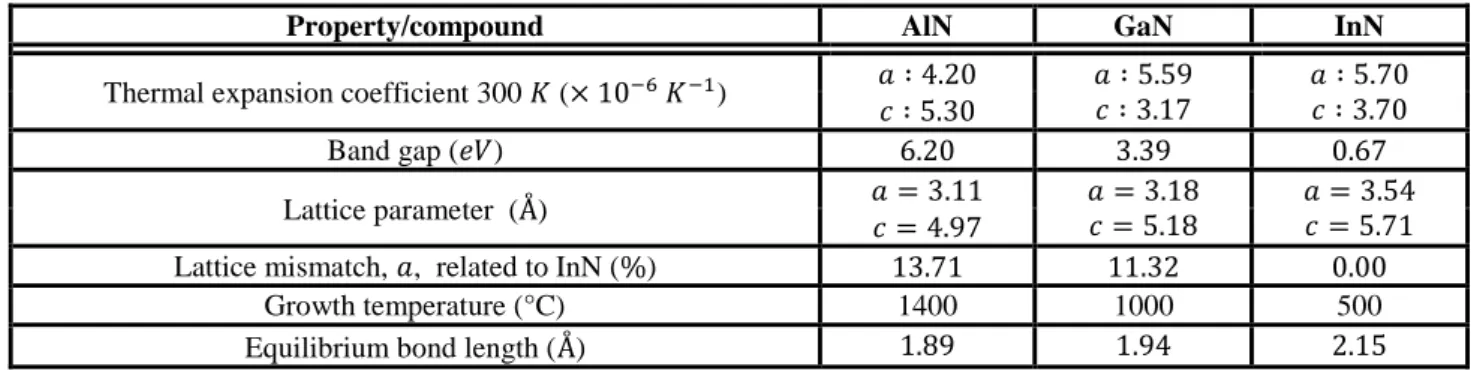
Table 1. Relevant properties of III-N compounds.
Property/compound AlN GaN InN
Thermal expansion coefficient 300 𝐾 (× 10−6 𝐾−1) 𝑎 ∶ 4.20 𝑎 ∶ 5.59
𝑐 ∶ 3.17 𝑎 ∶ 5.70 𝑐 ∶ 3.70 𝑐 ∶ 5.30
Band gap (𝑒𝑉) 6.20 3.39 0.67
Lattice parameter (Å) 𝑎 = 3.11 𝑐 = 4.97 𝑎 = 3.18 𝑐 = 5.18 𝑎 = 3.54 𝑐 = 5.71
Lattice mismatch, 𝑎, related to InN (%) 13.71 11.32 0.00
Growth temperature (°C) 1400 1000 500
Equilibrium bond length (Å) 1.89 1.94 2.15
This has been more successful for InGaN and AlGaN at least for small In and Al concentrations with the production of light emitting diodes and lasers [20]. However, in the case of InAlN, even at the lattice match point to GaN (In~18-19%), increasing the layer thickness leads to crystalline degradation
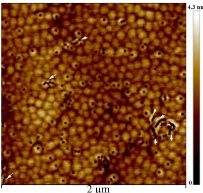
5 as has been reported [10-12]. As can be seen in figure 1, which is a 2x2 µm AFM image, for a layer thickness of 50 nm, the V defects (black dots) density is 3.6*109cm-2. This slightly smaller than reported in the 100 nm layer grown of a free standing GaN of reference 12, where their density was 4.5*109cm-2, which was 100 higher than the density of the threading dislocation present inside substrate. In our sample as shown by the arrows, many of the V-defects have already started to coalesce and form trenches.
Figure 1. InAlN/GaN layer grown by MOVPE 50 nm thickness, coalescing V-defects are shown by arrows.
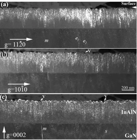
The connection of the V-defects to the threading dislocations is better revealed by TEM, and as can be seen in figure 2, which exhibits weak beam images of a InAlN layer of 336 nm nominal thickness, there are 2 edge, 1 mixed and 1 screw type threading dislocations from the GaN template [21]. From this figure, it can be seen, that in this sample, there are, neither basal [22] nor prismatic stacking faults [23], which would be in contrast in figure 2b. We also eliminate the presence of inversion domains [24], which should be visible in figures 2b and 2c. Obviously, there are no misfit dislocations at the AlInN/GaN interface as they also should be in contrast in figures 2a-c depending on their Burgers vectors. As clearly visible, all the dislocations that cross the interface lead to the formation of V defects at the layer surface (see arrows and V). In this projected area of the surface, at least 30 V defects are present, meaning that the 3 present dislocations contribute only for 10% to their total density. Therefore, the largest majority of the V defects formed inside the AlInN layer in agreement with the AFM observations of reference 12.
6
Figure 2. Weak beam images of a 336 nm nominal thickness InAlN/GaN layer of 19% indium composition, a) g=112̅0
image showing a (e) and a+c (m) dislocations, b) g=101̅0 image which underlines possible stacking faults, c) g=0002 image in which a+c (m) and c (s) are visible
As can be seen, the underlying GaN template has a uniform contrast; on top, the ternary layer images exhibit multiple changes in brightness, which correspond to local deformation and disorder. Clearly, the deviations are highest toward the surface of the layer. They start randomly along the [0001] growth direction and can even start at the interface with GaN. Therefore, this AFM and conventional transmission electron microscopy analysis shows that the spontaneous crystalline degradation of the layers appears to be dominated by a systematic formation of V defects which takes place randomly along the growth direction. This is clearly not due to the coalescence of growth hillock as was previously assumed. It is therefore most interesting to search for other possible mechanisms that could lead to their formation, and this is the main reason to undertake the following theoretical investigation.
IV.
Defective surface and stability
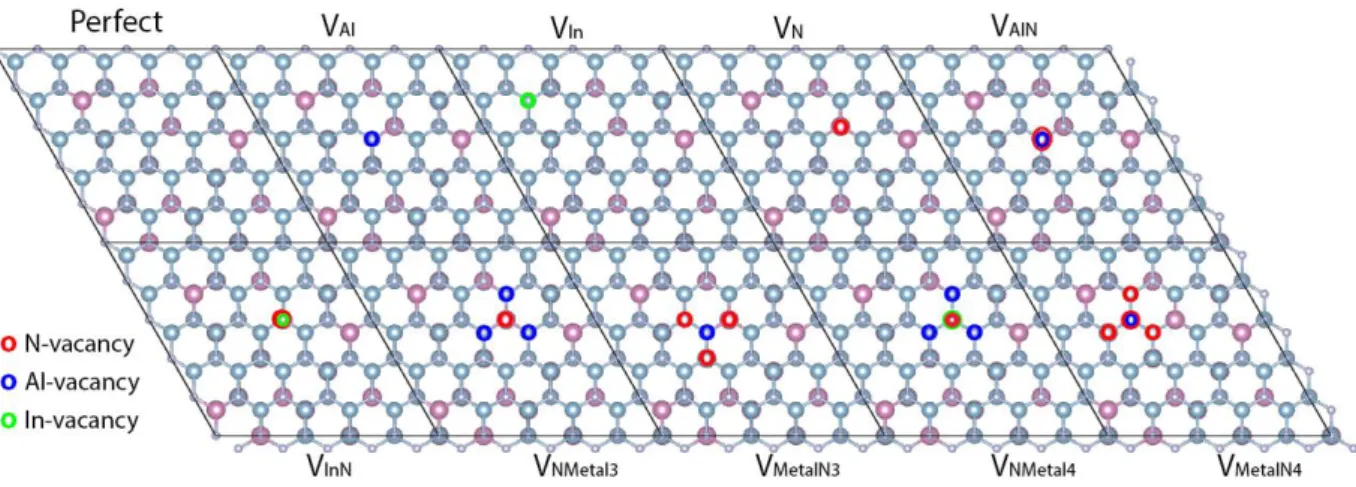
We considered the point defects in the {0001} InAlN (N- and Metal-polar) surface area. They include Al (𝑉𝐴𝑙), In (𝑉𝐼𝑛), and N (𝑉𝑁) single vacancies, AlN, InN double vacancies along the c-axis (𝑉𝐴𝑙𝑁, 𝑉𝐼𝑛𝑁), as well as vacancy complexes involving the neighbor atoms i.e (𝑉𝑁𝑀𝑒𝑡𝑎𝑙3, 𝑉𝑀𝑒𝑡𝑎𝑙𝑁3), and (𝑉𝑁𝑀𝑒𝑡𝑎𝑙4, 𝑉𝑀𝑒𝑡𝑎𝑙𝑁4). In this way, 10 initial configurations have been generated and relaxed using ab-initio calculations, the corresponding most stable ones are reported in figure 3 for the N-polar (0001̅) case, of course, we have the same defects at the Metal-polar surface.
7
Figure 3. The atomistic configurations of the investigated defects shown in the case of the (0001̅) InAlN surface.
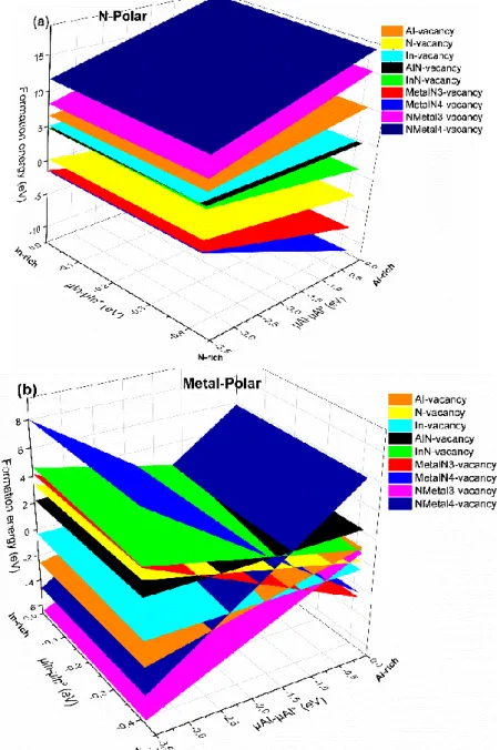
We have investigated the stability of the various defects (vacancy and complex vacancies) at the InAlN surface, as a function of the Al and In chemical potentials. Figure 4 shows the formation energy for the 10 surface configurations above in the two cases (N- and Metal-polar). For the highest µ𝐴𝑙
value, i.e., in Al-rich conditions, the lowest defect formation energy is the InAlN surface containing the MetalN4-vacancy (blue surface) for N-polar and MetalN3-vacancy (red surface) for metal-polar. Consequently, under the Al-rich conditions, the MetalN4-vacancy and MetalN3-vacancy have lower defect formation energy than that of the Metal-vacancy, which means that once a Metal-vacancy is formed, the N atoms around it may not be stable any more. Decreasing µ𝐴𝑙 to N-rich condition and for
all range of µ𝐼𝑛, the most stable surface becomes what has a Nmetal3-vacancy (Magenta surface) for
Metal-polar and still the
MetalN4-vacancy
for N-polar. The formation energy of small defects becomes higher as can be seen from Fig. 4, and the formation energy of one atom vacancy is larger than that of three or four atoms vacancy for all the chemical potentials range. Some of the defects have negative formation energies in the whole In and Al chemical potentials range, which indicates that the defective InAlN surfaces are more stable than the perfect ones.8
Figure 4. The formation energies of the point defects versus aluminum and indium chemical potentials for (a) N-polar and
(b) Metal-polar, the corresponding perfect surfaces were taken as references.
Considering the most stable surface defects as seen in figure 4 (𝑉𝑁𝑀𝑒𝑡𝑎𝑙3, 𝑉𝑀𝑒𝑡𝑎𝑙𝑁3 for metal-polar and 𝑉𝑀𝑒𝑡𝑎𝑙𝑁4 for N-polar surface), we now focus on how they can influence the adsorption and diffusion of In and Al on InAlN surfaces.
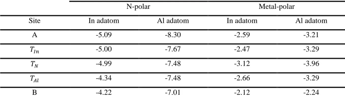
V. Adsorption of In/Al atom on InAlN surface
At the Metal- and N-polar (0001) surfaces, we considered In and Al above-surface sites: i) a top site above a N atom (𝑇𝑁), ii) above a metal atom (𝑇𝑚𝑒𝑡𝑎𝑙= 𝑇𝐴𝑙 𝑜𝑟 𝑇𝐼𝑛), iii) bridge site above the middle of Al-N bond (B), and iv) the hollow site in the hexagonal center (A), as shown in figure 5.
9
Figure 5. Schematic top view of the (0001̅) AlN surface, the blue atoms are Al, and the grey nitrogen, the four initial
positions of the Al (In) adatom can be seen (TN(metal) above a nitrogen (metal) atom, A along the 63 of the wurtzite structure,
and B lies above the saddle point between N-metal).
The calculated adsorption energies of In and Al adatoms on N-polar and Metal-polar InAlN surface are shown in Table 2. As can be seen, the In and Al atom in site A is more stable than in the other sites for the N-polar. For the metal-polar, the 𝑇𝑁 site is the most stable with an energy of -3.12 and -3.96 eV
for In and Al adatom, respectively.
Table 2. Calculated adsorption energies for In and Al adatoms on the N-polar and Metal-polar InAlN surface Adsorption energy (eV)
N-polar Metal-polar
Site In adatom Al adatom In adatom Al adatom
A -5.09 -8.30 -2.59 -3.21
𝑇𝐼𝑛 -5.00 -7.67 -2.47 -3.29
𝑇𝑁 -4.99 -7.48 -3.12 -3.96
𝑇𝐴𝑙 -4.34 -7.48 -2.66 -3.29
B -4.22 -7.01 -2.12 -2.24
All the possible positions for the In (Al) adsorption around the point defects were considered. The absolute values of the adsorption energies of the In (Al) on the defective InAlN surface are increased (decrease) compared with those on the perfect one for the N-polar. This is also the case when there are more than one metal-vacancy (NMetal3-vacancy) for metal-polar surface. For example, the adsorption energy for the In (Al) on the InAlN surface with 𝑉𝑁𝑀𝑒𝑡𝑎𝑙4 is -5.87 eV (-5.05 eV); this increases by ~0.78 eV (decreases by ~3.25 eV) compared with the -5.09 eV (-8.30 eV) for the In (Al) adatom on a perfect InAlN surface in the case of N-polar, and decrease ~0.11 eV (increase ~1.67 eV) from -3.23 eV (-2.29 eV) with 𝑉𝑀𝑒𝑡𝑎𝑙𝑁3 to -3.12 eV (-3.96 eV) for the perfect surface (metal-polar). Therefore, the adsorption of In atom is more favorable than that of Al on these InAlN defective surfaces.
10
Table 3. Adsorption energies for In and Al adatoms on the most stable InAlN surface defects in the two polarity. Adsorption energy (eV)
Defect In adatom Al adatom
𝑉𝑁𝑀𝑒𝑡𝑎𝑙4 (N-polar) -5.87 -5.05
𝑉𝑀𝑒𝑡𝑎𝑙𝑁3 (Metal-polar) -3.23 -2.29
In the presence of the 𝑉𝑀𝑒𝑡𝑎𝑙𝑁4, the most stable site for the In and Al adsorption is the A site around
the vacancies (similar to the perfect surface) for N-polar surface. The In and Al adatom prefers to be adsorbed on the T site above the N vacancy when the 𝑉𝑀𝑒𝑡𝑎𝑙𝑁3 or 𝑉𝑁𝑀𝑒𝑡𝑎𝑙3 is present, similar to when
the In atom is adsorbed on the perfect Metal-polar surface.
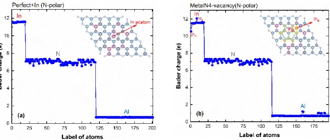
After discussing the defects stability and adsorption of In/Al atom on (0001) and (0001̅) InAlN surfaces, the charge transfer at the stable surface defect was investigated by means of Bader charge analysis. For the perfect surface (fig. 6a) with the adsorption of one In atom, the neighbouring nitrogen atoms display 7 e on average which is a gain of 2 e in comparison to the isolated N atom (5 e); the adsorbed atom, In (Al) atom loses 1.5 e (2.3 e). Even with the high electronegativity of N (3.04), which is larger than that of Al (1.61) or In (1.78), there is a clear difference in the behavior of the In-N and Al-N bounds, aluminum nitride is the most stable of the three nitride, and indium nitride is the least stable [25].
Figure 6. Bader charge analysis of individual In, Al, N atoms for InAlN N-polar perfect surface (a) and with
metalN4-vacancy (b).
As was recently shown, the bond is rather ionic in AlN, whereas it is partially covalent in InN [16]. On the defective InAlN surface, the In adatom (Ina in fig. 6b), partially transfers its valence electron (1 e)
to the metallic atoms (Al, Ins) located around the vacancies in the first and second layers (the atoms
have been underlined with a yellow cross in fig. 6b), the In2 gains ~0.5 e whereas Al atoms gains on
11 charge, therefore, this coulomb charging reinforces the adsorption and the possible next step to formation of bonds at the surface.
VI. Diffusion of In/Al adatom on InAlN surface
The diffusion of atoms on a surface is one of the key parameters controlling growth rate, material quality, and surface morphology during epitaxial growth. However, monitoring and analyzing the surface diffusion processes are relatively difficult using experimental methods [26], hence the theoretical investigation of surface diffusion pathways and diffusion barriers may provide important information relevant to the growth of InAlN layers.
In this section, we discuss the role of the most stable defects on the diffusion of In and Al, as well as on the possible aggregation of indium. As seen above, they are, for the metal-polar InAlN surface, 𝑉𝑁𝑀𝑒𝑡𝑎𝑙3 𝑎𝑛𝑑 𝑉𝑀𝑒𝑡𝑎𝑙𝑁3 in In-, N-rich and Al-rich condition, respectively. Indeed, the
𝑉𝑀𝑒𝑡𝑎𝑙𝑁4 is the most stable for the N-polar InAlN surface. The diffusion pathway of the In (Al) atom
was determined by moving the In (Al) atom with a small constant distance on a perfect metal polarity InAlN surface from TN to the next and the total energy was recorded at each step. In the process, the
atom was constrained in the direction along the path, and was free to move in the perpendicular directions, which enables it to find the minimum energy position. As shown in insert of fig. 7(a), the optimal pathway, goes through the A site and the calculated diffusion barriers (fig 7) for the In (red) and Al (blue) atom on the perfect (0001) InAlN surface is 0.439 eV and 0.871 eV, respectively.
The two diffusion paths for the In (Al) diffusion at the (0001) InAlN surface with the most stable defect (𝑉𝑀𝑒𝑡𝑎𝑙𝑁3, 𝑉𝑁𝑀𝑒𝑡𝑎𝑙3), and the energy curves as a function of relative diffusion coordinates are shown in Fig. 5(b, c). As can be seen, the situation is very simple for the diffusion of the indium atom with a single barrier in the two cases. The energy barrier increases by ~ 0.203 eV compared with the perfect surface in the presence of MetalN3-vacancy (fig. 7(b)), and decreases ~ 0.055 eV in the case of NMetal3-vacancy (fig. 7(c)).
For the Al atom, the process is more complex, the migration pathway requires the Al to first go from 𝑇𝑁 to A site with a diffusion barrier of 1.05 eV (𝑉𝑀𝑒𝑡𝑎𝑙𝑁3) and 0.75 eV (𝑉𝑁𝑀𝑒𝑡𝑎𝑙3), respectively. Subsequently, it should diffuse from A to the next 𝑇𝑁 position (close to the defect) with a barrier of 0.2 eV and 1 eV for 𝑉𝑀𝑒𝑡𝑎𝑙𝑁3 𝑎𝑛𝑑 𝑉𝑁𝑀𝑒𝑡𝑎𝑙3, respectively.
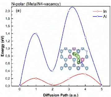
On the perfect (0001̅) InAlN surface (N-polar), the stable adsorption site for In (Al) adatom is site A (fig. 5d). As shown in the insert, the diffusion of In(Al) goes from site A to the next across 𝑇𝑁, and the calculated diffusion barrier is 0.942 eV and 1.936 eV for In and Al atom, respectively. Therefore, for the two adatoms types, the diffusion barrier is larger on N-polar (0001̅) surface because, as seen above (Table 2], the adsorption energies are higher on this surface. In this case, the corresponding most stable 𝑉𝑀𝑒𝑡𝑎𝑙𝑁4 defect induces a quite large decrease of energy barrier, from 0.942
12 eV (perfect surface) to 0.2 eV, in the case of In, as can be seen from the energy curves in fig. 7(e). In the case of Al, we still end up with a complex process with two different barriers along the diffusion path, first as 1.4eV and then 1.7 eV.
From these results, we can conclude that the point defects may enhance the diffusion of In, obviously, this is not true for Al atom for which the energy barriers are always high, probably because of its large adsorption energy.
13
Figure 7.Diffusion of In in perfect In(18%)AlN and with defects. Energy curves for In (red curve) and Al (blue curve) ions diffusion on (a) perfect InAlN surface (metal-polar) and the one with (b) MetalN3-vacancy (metal-polar) (c) NMetal3-vacancy(metal-polar), (d) perfect N-polar of InAlN surface, (e) MetalN4-vacancy (N-polar). The corresponding diffusion path (green) is inserted in each case (Al: blue ball, N: gray ball and In: red ball).
VII. Towards In enrichment
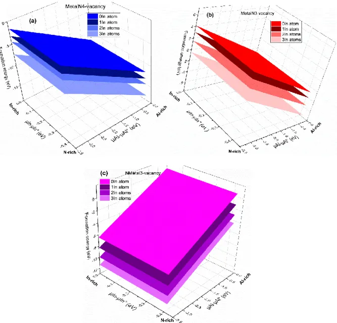
The remaining question for the building up of aggregates is to determine if the In atoms on the surface will be able to naturally diffuse towards the defects. To this end, we moved one, two and three In atoms on the surface from their random position, and made them substitute the Al atoms around the defect. Then, we calculated the formation energy for each case (three cases in all) in order to find out if these three cases are more stable. As can be seen in fig. 8, the formation energies are lowest when the In atoms are brought to settle around the defects, the surface energy decreases more and more with the number of In atoms around the vacancies. The InAlN surface become more stable in the case of three In atoms represented by the light blue, light red and light purple in the figure for MetaN4-vacancy (N-polar), MetalN3-MetaN4-vacancy and NMetal3-MetaN4-vacancy (Metal-polar), respectively. We can therefore conclude that In-rich regions may form due to the presence of these surface defects.
14
Figure 8. The formation energies of the most stable defects as a function of aluminum and indium chemical potentials for (a)
MetalN4-vacancy (N-polar), (b) MetalN3-vacancy (Metal-polar) and (c) NMetal3-vacancy (Metal-polar) versus number (0-3) of In atoms around the defects. For all the cases, the surface with three In atoms around the vacancy sites exhibits the lowest energy.
The same procedure has been carried out in the bulk part of the InAlN alloy; in this case, the energy evolution of the supercell has been followed when we approach an In atom towards a vacancy site, as shown the figure 9 one In atom has moved according to two paths 1-3 and 2-3. In this case, as well, the energy of the system decreases when the In atom diffuses towards the vacancy by 1.27 eV and 1.24 eV for path 1-3 and 2-3, respectively.
15
Figure 9. InAlN structure viewed along [0001], the VN position is shown by the black asterisk *, the numbers 1, 2 and 3
indicate the indium position.
VIII. Discussion
From the AFM and TEM investigations it is now clear that the crystalline degradation of lattice matched InAlN layers on GaN is governed by the generation of V-defects and their rapid multiplication when the layer thickness is increased. On top of low dislocation (4∙107
cm-2) FS GaN substrates the V-defects density reaches two orders of magnitude when the layer thickness was 100 nm [12]. Obviously, from the TEM observations in figure 2, the degradation is independent of the threading dislocations [11]; it takes place randomly all along the InAlN layer thickness. Therefore in contrast to previous reports [12] there is no critical thickness where it is initiated. This is probably different to what has been reported as a critical thickness from which some phase separation has been deduced using Rutherford Backscattering analysis [10], which probably corresponds to some level of thickness where it becomes detectable. Moreover, the AFM clearly show the 3D growth of the InAlN with the formation of hillock, however, the V-shape whose increases steadily with the layer thickness form exactly at the top of the hillocks, and not at their coalescence, so the possible phase separation may not be directly related to the inclined lattice planes of the coalescing growth fronts [12]. Our present work attempts to take into account the intrinsic properties of the various atoms that are interacting during the growth process. Our recent analysis of the InN-AlN phase diagram [6] revealed that even at the lattice match to GaN, the growth of this compound takes place in phase separation zone. For instance, in ultrathin In0.72Al0.28N layers deposited on AlN [27], and thus first stabilized by
the large compressive strain [6], a subsequent thermal annealing leads to a random decomposition of the alloys by formation of 2-3 nanometer size domains which grow larger with annealing temperature and time [27]. This is in agreement with our recent work on the possible role of the nitrogen vacancies in the formation of indium rich areas inside InAlN, as well as the TEM observations which reported cluster of similar size [28]. The above results which show that the {0001} InAlN growing surface should be more stable when it contains defects bring a clear new insight on these observations. The
16 complex defects appear to be the most energetically stable, they are AlN3-, NAl3- vacancy for metal-polar and AlN-4 vacancy for N-metal-polar surfaces, respectively. The above surface diffusion analysis of In/Al adatoms shows that the In atoms should diffuse easier than the Al atom on the defective surface, the diffusion barrier decrease (increase) in case of In (Al) adatom and the adsorption energy for Al is the highest. Moreover, substituting the Al atoms initially located around the vacancy by In atoms minimizes the energy of the system. Therefore, during the growth, the formation of indium clusters around these defects which should be randomly distributed could be a mechanism that predominates in the observed phase separation.
The above observations may also be used to explain the surface morphology of the InAlN layers, as to the presence of the V-defects. According to Chen et al., threading dislocations are considered to be at the origin of defects. Other possibilities for the origin of defects have been proposed. The V-defect density in GaN increases dramatically with an increase in the concentration of impurities in InAlN layers [29]. Based on our observation and on the above results, the V-defects are not predominantly due to threading dislocations or to other structural defects such as a stacking mismatch boundary or a stacking fault [28]. If we consider closely the investigated surface defects, they may also be seen, on a growing InAlN surface, as the nuclei of V-shaped defects. For instance, if we take 𝑉𝑀𝑒𝑡𝑎𝑙𝑁3 defect, which is the most stable on a metal-polar InAlN surface (fig. 10a), it may be a starting point for the nucleation of a V-defect as follows. The In-rich region could be formed as shown in fig 10(b) at the V-defect, as the In atoms diffuse easier than Al atoms to the vacancies. The diffusion barrier decreases in case of defective InAlN surface for In, therefore the surface becomes more stable when more In indium atoms replace Al ones around the defects sites. In subsequent layers during the growth, the V-pit forms with the initial concave and convex facets as has been proposed in reference 12. Subsequently, due to the lower growth rate perpendicular to {10-11} surfaces (vs) than along vertical axis (vc), the V-shape defect increases in size with the growth progress, as shown in fig. 10(b). With the In segregation at the beginning of V-defects, an In-poor or In-rich InAlN areas may form in agreement with the experimental observation [11, 12].
Figure 10.Schematic diagram of the growth on InAlN defective surface (a) The early stage of the surface with 𝑉𝑀𝑒𝑡𝑎𝑙𝑁3
defect (b) The final stage with a large V-defect formed at the In-rich region. The blue, red and silver balls represent Al, In and N atoms, respectively.
17
IX. Conclusion
In summary, we have carried out a theoretical investigation of the surface structure and adatom kinetics for wurtzite InAlN and their contribution on the crystallographic degradation in nearly lattice matched InAlN (In=18-19%) on (0001) GaN. In agreement with the AFM observation that there is an extensive formation of the V-defects when the layer thickness increases, as well as the TEM observations that show the crystallographic degradation, it is found that the defective InAlN surface is energetically more stable than the perfect one. Moreover, the adsorption energies of In on the defective InAlN (MetalN4-vacancy for N-polar and NMetal3-vacancy for Metal-polar) surface increase compared to those on the perfect one. This means that the In will attach more to such surface which eventually lead to phase separation with In-rich and In-poor regions in the form of initial V-defects. The presence of vacancies is shown to favor the diffusion of In adatoms towards it as the corresponding energy barrier and the formation energy are decreased. At the growth surface, the degradation started at the stable defect nuclei terminates in the form of V defects, which characterize the final morphology. These findings not only provide insight into the degradation mechanism of lattice matched InAlN to the substrate GaN, but may also be helpful towards the understanding of the growth of In-containing III-nitrides.
Acknowledgments
This work has been carried out through regional Normandie project RIN2018 PLACANANO convention N°: 18E01651. The calculations were carried out in the “Centre Régional Informatique et d’Applications Numériques de Normandie ‘CRIANN’” (www.criann.fr) under Project No. 2016009. References
[1] J.-F. Carlin, M. Ilegems, Appl. Phys. Lett. 83 (2003) 668-670. [2] M. A. Khan, S. Shur, Q. Chen, Appl. Phys. Lett. 68 (1996) 3022. [3] J. Kuzmik, IEEE Electron Device Lett. 22 (2001) 510.
[4] F. Medjdoub, J. Carlin, Elec. Elect. Eng. J. 2 (2008) 1. [5] P. Ruterana, G. Nouet, Phys. Stat. Sol. (b) 227 (2001) 177.
[6] R. Mohamad, A. Béré, J. Chen, P. Ruterana, Phys. Stat. Sol (a) 214 (2017) 1600752.
[7] R. Mohamad, A. Béré, V. Hounkpati, P. Gamarra, J. Chen, P. Ruterana, Phys. Stat. Sol. (b) 255 (2018) 1700394.
[8] C. S. Gallinat, G. Koblmüller, J. S. Brown, J. S. Speck, J. Appl. Phys. 102 (2007) 064907.
[9] R. Butté, J.-F. Carlin, E. Feltin, M. Gonschorek, S. Nicolay, G. Christmann, D. Simeonov, A. Castiglia, J. Dorsaz, H. J. Buehlmann, S. Christopoulos, G. Baldassarri Höger von Högersthal, A. J. D. Grundy, M. Mosca, C. Pinquier, M. A. Py, F. Demangeot, J. Frandon, P.G. Lagoudakis, J. J. Baumberg, N. Grandjean, J. Phys. D 40 (2007) 6328.
18
[10] A. Redondo-Cubero, K. Lorenz, R. Gago, N. Franco, M.-A. di Forte Poisson, E. Alves, E. Munoz, J. Phys. D 43 (2010) 055406.
[11] Z. T. Chen, K. Fujita, J. Ichikawa, T. Egawa, J. Appl. Phys. 111 (2012) 053535.
[12] G. Perillat-Merceroz, G. Cosendey, J.-F. Carlin, R. Butté, N. Grandjean, J. Appl. Phys. 113 (2013) 063506. [13] G. Kresse, J. Furthmüller, Phys. Rev. B 54 (1996) 11169.
[14] J. P. Perdew, K. Burke, M. Ernzerhof, Phys. Rev. Lett. 77 (1996) 3865. [15] P. E. Blöchl, Phys. Rev. B 50 (1994) 17953.
[16] R. Mohamad, J. Chen, P. Ruterana, Comput. Mater. Sci. 172 (2020) 109384. [17] H. J. Monkhorst and J. D. Pack, Phys. Rev. B 16 (4) (1976) 1748–1749. [18] A. Vilalta-Clemente, PhD, University of Caen, (2012).
[19]Y. Yue, Z. Hu, J. Guo, B. Sensale-Rodriguez, G. Li, R. Wang, F. Faria, B. Song, X. Gao, S. Guo, T. Kosel, G. Snider, P. Fay, D. Jena, and H. G. Xing, Japanese Journal of Applied Physics 52 (2013) 08JN14.
[20] S. Nakamura, Science 281, 956 (1998).
[21] V. Potin, P. Ruterana, G. Nouet, R.C. Pond, and H. Morkoç, Phys. Rev. B 61, 5587 (2000). [22] V. Potin, P. Ruterana and G. Nouet, J. Phys. Condensed Matter 12, 10301 (2000).
[23] P. Ruterana, B. Barbaray, A. Béré, P. Vermaut, A. Hairie, E. Paumier, and G. Nouet, A. Salvador, A. Botchkarev, and H. Morkoc, Phys. Rev. B 59, 15917-15925 (1999).
[24] V. Potin, G. Nouet, P. Ruterana, Phil. Mag. A79, 2899 (1999).
[25] B. Lacroix, M. P. Chauvat, P. Ruterana, K. Lorenz, E. Alves, A. Syrkin, J. Phys. D: Appl. Phys. 44 (2011) 295402.
[26] V. Jindal, F. Shahedipour-Sandvik, J. Appl. Phys. 105 (2009) 084902.
[27]J. Palisaitis, C.-L. Hsiao, L. Hultman, J. Birch P. O. Å. Persson, Sci. Rep. 7 (2017) 44390.
[28] R. Mohamad, M.- P. Chauvat, S. Kret, P. Gamarra, S. Delage, V. Hounkpati, C. Lacam, J. Chen, P. Ruterana, J. Appl. Phys. 125 (2019) 215707.
![Figure 9. InAlN structure viewed along [0001], the V N position is shown by the black asterisk *, the numbers 1, 2 and 3 indicate the indium position](https://thumb-eu.123doks.com/thumbv2/123doknet/13593792.423248/16.892.124.352.110.333/figure-inaln-structure-position-asterisk-numbers-indicate-position.webp)
