Dielectric Spin Coating Characterization, Modeling, and Planarization
Using Fill Patterns for Advanced Packaging Technologies
by
Christopher Ilic Lang
S.B., Electrical Engineering and Computer Science, MIT, 2015
Submitted to the
Department of Electrical Engineering and Computer Science in Partial Fulfillment of the Requirements for the Degree of Master of Engineering in Electrical Engineering and Computer Science
at the
Massachusetts Institute of Technology January 2017
© 2017 Massachusetts Institute of Technology. All rights reserved.
Author: ____________________________________________________________
Department of Electrical Engineering and Computer Science January 15, 2017
Certified by: ____________________________________________________________
Duane S. Boning Professor of Electrical Engineering and Computer Science Thesis Supervisor
Accepted by: ____________________________________________________________
Christopher Terman Chairman, Masters of Engineering Thesis Committee Department of Electrical Engineering and Computer Science
3
Dielectric Spin Coating Characterization, Modeling, and Planarization
Using Fill Patterns for Advanced Packaging Technologies
by
Christopher Ilic Lang
Submitted to the Department of Electrical Engineering and Computer Science January 15, 2017
In Partial Fulfillment of the Requirements for the Degree of Master of Engineering in Electrical Engineering and Computer Science
Abstract
Redistribution layers (RDLs) are separate packaging layers dedicated to connecting dies with each other, and to external I/O ports in advanced 2.5D packaging technologies. These layers can be made smaller than the bulky metal traces in conventional substrate packaging, reducing electrical delay and power consumption. Currently, the damascene process is the most common method to create the copper traces in RDLs. However, due to the required inclusion of chemical mechanical polishing (CMP), this process is significantly more expensive than semi-additive electrochemical plating (ECP) and dielectric spin-coating (DSC) processes. The semi-additive techniques are typically avoided as, without CMP, they suffer from thickness variations following the fabrication of each layer. As multiple layers are fabricated, these variations compound, and can result in a structure with significant topographical and electrical performance concerns.
In this thesis, we model and predict the surface non-uniformities resulting from the DSC process applied to underlying topographies, and propose dummy fill and cheesing patterns which control the variations of the DSC process. We first design test vehicles (TVs) which represent topographies common in RDLs, most notably the copper lines and vias, and use these to experimentally determine the thickness variations caused by each process. We then develop empirical models based on these results. The DSC process is modeled as a convolution between the underlying topography (typically the copper lines) and an appropriately chosen impulse response. Finally, we present dummy fill and cheesing patterns that have the potential to control the variations of both processes for any arbitrary layout.
Thesis Supervisor: Duane S. Boning
5
Acknowledgements
Firstly, I would like to thank my research advisor, Duane Boning, for guiding me through my Master’s program. His advice has been instrumental in producing the following work, and his patience and enthusiasm have made the process a pleasure. I couldn’t ask for a better advisor, and look forward to working together in the future. Secondly, I would like to thank my parents, Jeffrey Lang and Marija Ilić. Both have given me invaluable advice and inspiration throughout my life, and I owe them everything that I have. I wouldn’t be where I am today without having them as parents. I would also like to thank all of the MTL staff, and in particular Vicky Diadiuk, Kurt Broderick, Dave Terry, Paul Tierney, Scott Poesse, Robert Bicchieri, Bernard Alamariu, and Paudely Zamora, who have each helped me during my research. Finally, I would like to thank Taiwan Semiconductor Manufacturing Company, who has in part sponsored this work, and in particular C.-C. Hsieh, J. Hu, J. Ho, C.-H. Tung, C.-H. Steven Lin, H.-P. Pu, and C.H. Yu all of whom have provided feedback throughout the process.
7
Contents
Chapter 1: Introduction ... 10
1.1) Redistribution Layers in Advanced Packaging ... 10
1.2) Existing DSC Models ... 12
1.3) Thesis Organization ... 13
Chapter 2: Experimental Setup and Results... 15
2.1) Test Vehicle Design and Fabrication ... 15
2.1.1) Initial TV Design ... 16
2.1.2) Transitions ... 16
2.1.3) Vias ... 18
2.1.4) Dimensions ... 19
2.1.5) Material Choice ... 19
2.1.6) TV Fabrication and Characterization ... 21
2.2) Spin Coating Results ... 21
2.2.1) Feature Scale Variation ... 22
2.2.2) Long Range Variation ... 23
2.2.3) Tip Pinch-Off and Measurement Fidelity ... 25
Chapter 3: Modeling ... 29
3.1) Model Form ... 29
3.2) System Impulse, Step, and Frequency Response ... 29
3.2.1) Initial Fit ... 30
3.2.2) Updated Fit ... 33
3.3) Model Predictions ... 36
3.4) Model Accuracy ... 38
3.5) Model Extremal Cases ... 40
3.5.1) Penalty Function for Extremal Cases ... 41
3.6) Model Trends ... 45
3.7) Impact of Updated Fit and Coefficient Significance ... 46
3.8) Closed Form Analysis ... 49
3.9) Existing DSC Modeling Revisited ... 54
3.10) Effects of Feature Location and Orientation ... 56
8
3.11.1) Experimental Results ... 58
3.11.2) Hirasawa Analysis ... 61
3.12) Coatings Over Non-Binary Topographies ... 64
3.13) Model Sensitivity ... 70
3.14) Two Dimensional Model Form ... 72
Chapter 4: Model Applications ... 80
4.1) Design Guidelines... 80
4.2) Fill Pattern ... 82
4.3) Fill and Cheesing Patterns ... 84
Chapter 5: Conclusion and Future Work ... 93
5.1) Contributions ... 93
5.2) Future Work ... 95
References ... 97
Appendix A: Experimental Scans and Predictions ... 100
T = 8 µm ... 100
T = 13 µm ...110
Appendix B: Feature Scale Results and Predictions ... 121
T = 8 µm ... 121
10
Chapter 1: Introduction
This thesis explores some of the problems and potential solutions associated with the dielectric spin coating process when used in redistribution layer fabrication. In particular, we focus on modelling and controlling the non-planar surfaces resulting from coating existing topographies. In this chapter, we introduce the necessary background information and give an overview of the thesis as a whole. In Section 1.1 we review the necessary background information regarding integrated circuit (IC) packaging, redistribution layers fabrication, and the spin coating process. We then briefly cover the existing spin coating process models and their limitations in Section 1.2. While these existing models are only briefly discussed, we later return to them in Sections 3.9 through Section 3.11. Finally, we describe the overall structure of the thesis in Section 1.3.
1.1) Redistribution Layers in Advanced Packaging
Modern IC design is commonly driven by improving the electrical performance, cost, power efficiency, and system integration of the devices fabricated. Traditionally, designers and manufacturers have focused on improving these characteristics within an individual die. However, as the capability of the individual die continues to improve, a need for improved also packaging arises [1, 2]. Bulky metal traces in conventional substrate packaging, such as ball grid arrays (BGAs) and quad flat packages (QFP), limit interconnect density, are electrically slow, and consume significant power [3]. If not considered, these limitations can bottleneck the IC and system performance as a whole. Redistribution layers (RDLs) are separate packaging layers that use copper interconnects to connect multiple die to one another, as well as to external I/O ports, as seen in Fig. 1. Additionally, this form of packaging, known as 2.5D integration, can be more thermally and mechanically reliable compared to fully stacked, 3D integration [4], and can be more easily integrated with existing designs [5], making it a practical solution to current packaging needs.
11
Figure 1: Redistribution layer connecting adjacent die.
Currently, the most common fabrication method for multi-level RDLs is the damascene process [5]. In this process, the dielectric is first deposited, then etched where copper lines will be formed. Copper is then deposited across the entire structure. Finally, chemical-mechanical polishing (CMP) removes the unwanted copper from above the dielectric, leaving a planar surface with embedded copper interconnect lines and vias.
Figure 2: Damascene (left) vs. semi-additive (right) RDL fabrication.
While the damascene process produces well-formed structures, it is also costly [6]. A critical factor in adopting the 2.5D integration technology will be reducing this cost [5]. An alternative, semi-additive metallization process is a potential improvement, as it does not require CMP [2]. In this process, copper lines are first grown using semi-additive electro-chemical plating
12 (ECP). Then the dielectric is deposited, typically using dielectric spin coating (DSC). Finally, parts of the dielectric are etched to reveal the copper lines below. Both the damascene and semi-additive processes can be seen in Fig. 2.
While potentially less expensive than the damascene process, RDLs made using the semi-additive metallization process suffer from thickness variations, as the process does not use CMP [7]. Instead, as multiple layers are fabricated, thickness variations accumulate and can reduce the performance of the RDL structure. An illustration of this effect can be seen in Fig. 3. Additionally, large thickness variations across a layer require a large depth of focus in subsequent lithography steps, thus reducing the possible resolution and impacting the feature size for those layers [2, 7].
Figure 3: Incorrectly fabricated RDL. Thickness variations in the ECP and DSC cause uneven final topography.
In order to better understand the limitations of the conventional metallization process, this thesis explores a new model that predicts the resulting thickness variations after DSC based on the underlying topography. Using this model, metal layers can be designed such that the thickness variations after spin coating is limited, thus eliminating the need for CMP and reducing the fabrication cost of RDLs in advanced packaging.
1.2) Existing DSC Models
An existing DSC process model comes from Stillwagon and Larson [8], who predict the topography of a liquid dielectric during spin coating. However, this model suffers from two major problems. First, evaporation has a significant impact on the final topography of DSC, and this is not included in the initial model. In order to incorporate evaporation, a “two-stage” model is further developed by Peurrung and Graves [9]. During the first stage of this model, drying is assumed to have no effect on the shape of the film profile. Then after a reaching equilibrium during spinning,
13 the evaporation is modeled as a fractional loss. While this is the predominant DSC model, this thesis later shows that for polyimides, and other dielectrics which require separate curing stages, this model cannot be applied. In these cases, the film is often level after spin coating, and the curing stage dominates the final topography.
A second major problem with the two-stage model is that is computationally infeasible to apply to the entire RDL. The model takes the form of a partial differential equation that must be solved using iterative methods. Applying this model to areas of 20mm x 20mm or larger, with feature sizes of 1 µm or less becomes computationally difficult, as there are approximately 400 million nodes. A DSC model is needed that can scale to larger areas.
A second model for the DSC process comes from Hirasawa et al. [10]. In this analysis, the authors focus on modeling the drying stage of the spin coating process. While more relevant to polyimides and other polymers that require separate curing stages, there are still significant differences between the Hirisawa model predictions and the experimental results presented in this thesis. It is believed that this discrepancy is due to simplifying assumptions used in the model, which are later explored in Section 3.11. Finally, the model again takes the form of a complex partial differential equation, limiting its feasibility for large scale applications.
1.3) Thesis Organization
The lack of an accurate and efficient model for the DSC process motivates further development. In this thesis, a newly proposed model is developed and compared to experimental results. Before presenting the model itself, the design and results of experiments used to develop and assess the model are presented in Chapter 2. This chapter begins in Section 2.1 by detailing the design and fabrication of Test Vehicles (TVs), structures which represent a range of topographies common in RDLs. After fabrication, the TV’s are coated with polyimide, and the resulting topographies are profiled and discussed in Section 2.2.
After discussing the experimental data, the predictive model for the process is presented in Chapter 3. The model is used to predict the profiles measured and presented in Chapter 2. The results of the model predictions are compared to the experimental data, and the model accuracy is quantified. Later in Chapter 3, the model is applied to two new types of underlying topographies, and its accuracy is examined. First, the models is used to predict coatings over structures with
14 multiple starting heights. Then, its form is expanded to two dimensions. Again, the results of the model in both cases are compared to experimental data. Chapter 4 then uses the results of the model to develop fill patterns which can limit the resulting dielectric surface variation of any existing RDL layout. Finally, Chapter 5 presents final conclusions and suggests future work.
15
Chapter 2: Experimental Setup and Results
In this chapter, we present the methodologies and results of our experimental findings used to develop the spin coating model. Section 2.1 details the development and final design of our Test Vehicle (TV). Here, we present both the layout of the structure, the fabrication techniques used, and the range of TV geometries used. Section 2.2 then presents experimental profiles of the spin coated TVs, and the feature scale and chip scale trends seen in these experimental profiles.
2.1) Test Vehicle Design and Fabrication
Here, the design and fabrication of the test vehicle is presented. A good TV includes structures common in RDLs, and the TV coated profiles are the primary data set used to develop and characterize the model. Therefore, the range of features present in the TV should not only represent those common in RDLs, but the TV features should be laid out in a way that facilitates the model development.
The most abundant and important features present in RDLs are the copper interconnects. Therefore, the TV is designed to include a large range of interconnect feature sizes. The geometry of each individual interconnect is defined by its line width and height, as illustrated in Fig. 5. While the line length also affects the coated profile, the profilometer used only measures height in one dimension, and thus the initial model only predicts these one dimensional coatings. For this reason, we use sufficiently long lines that reduce the effect of this second dimension (length), and do not initially consider its effect. We later expand our model to two dimensions in Section 3.14, which can then predict the coatings over lines of arbitrary lengths.
In addition to the geometry of each interconnect, the spacings of the interconnects are needed to define the entire RDL layout. Finally, the polyimide thickness is needed to define the entire coated RDL. These four parameters, height, width, spacing, and thickness (commonly abbreviated H, W, S, and T) are the main geometric parameters considered in this study. A common range of values for each of these variables is later defined and discretized. Finally, the TVs are designed, fabricated, and coated such that all combinations of these four discretizations are present.
16
2.1.1) Initial TV Design
The first iteration of the TV design aims to represent the major variables as simply as possible. This design consists of a matrix of uniform regions, where each region consists of parallel lines with a defined line width and line spacing. An overview of the initial TV design can be seen in Fig. 4 and an illustration of the uniform regions can be seen in Fig. 5. Along one axis of the TV, the line widths of the uniform regions increase, and along the other axis, the line spaces increase. This design ensures that there exists a uniform region for any combination of the defined line widths and spacings within each TV. Line height and polyimide thickness are not considered in this design, but are determined during the TV fabrication and subsequent coating. For this reason, multiple TVs are fabricated and coated such that there exists a range of combinations of line height and polyimide thickness. The TV layout, in combination with multiple TV fabrication runs, ensures that within the set of TVs, there exists a uniform region with each desired combination of the predefined line widths, spacings, heights, and polyimide thicknesses and that the ranges of interconnect dimensions common in RDLs are represented.
Figure 4: Initial TV layout showing matrix of uniform line width and line spacing regions.
Figure 5: Diagram of lines in within a uniform region.
2.1.2) Transitions
While the initial design contains all desired combinations of line spaces, widths, and heights, it neglects the transitions between regions. In the initial design considered above, the line widths and spaces monotonically increase along each axis, and there is little variety in the transitions between the regions. Increasing the variety of feature changes between regions allows
17 us to better observe the area of effect or spatial range of each process, and helps develop a more general model. Here a re-ordering of the initial design is developed that is intended to maximize the range of feature transitions in the RDL.
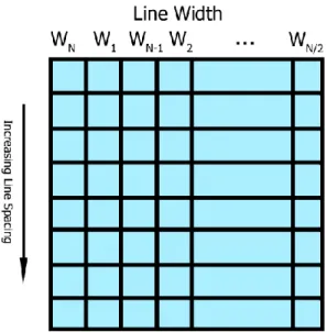
In order to maximize the range of line width transitions, a staggered ordering is used, as is illustrated in Fig. 6. Instead of monotonically increasing line width, the largest width is followed by the smallest width, followed by the second largest width, followed by the smallest largest, etc. This layout results in transitions of decreasing intensity, and maximizes the range of transitions present in the TV.
Figure 6: Staggered line widths. Note: 𝑊1 through 𝑊𝑁 refers to relative line width.
While this technique increases the range of transitions in line widths between regions, it does not increase the transitions in line spacings. Staggering both axes would not achieve this, as the directionality of the TV interconnects allows profiles to be measured in only one direction. In order to maximize the range of transitions for both line spacing and width, the design is split into two halves. Each half includes either staggered line spacing, or staggered line width, while the other parameter is kept monotonically increasing, as is illustrated in Fig. 7. Both halves of the design still include the same combinations of line widths and spaces; however, the width of each uniform region is reduced by a factor of two. This final modification allows for a more complete study of line width and space transitions, without increasing the total area of the TV, or reducing the total area devoted to each line and space combination.
18
Figure 7: Staggered line width and spaces. Again, 𝑊1 through 𝑊𝑁 and 𝑆1 through 𝑆𝑁 are relative line widths and spacings.
2.1.3) Vias
While copper lines account for the majority of the features in RDLs, copper vias are also present. For this reason, vias are included along the outer side of the TV. Both square and circular vias, as well as positive (raised), and negative (recessed) vias are included in the design. The inclusion of both positive and negative vias allows the same mask to be used for both positive and negative resists when fabricating the TV, and also gives additional information t can be considered during the model development. The final layout of the TV can be seen in Fig. 8.
19
2.1.4) Dimensions
The overall TV dimensions are 22mm x 22mm, as this is the maximum image field size of the Nikon stepper lithography system used at the MIT Microsystems Technology Laboratories (MTL). Structures larger than this require additional steps to fabricate, and this is not necessary for the TV design.
The line widths and spaces chosen range from 0.5 µm to 256 µm. This range is chosen as feature sizes smaller than 0.5 µm are not common in RDLs [2], and features spaced greater than 250 µm apart can be modeled as isolated features. Ten values, geometrically spaced from 0.5 µm to 250 µm, are used for the TV line widths and spaces. This gives each uniform region an area of 2 mm x 1 mm, and line width and spaces of 0.5 µm, 1 µm, 2 µm, 4 µm, 8 µm, 16 µm, 32 µm, 64 µm, 128 µm, and 256 µm. These values are also used for the via sizes, while the distances between the center of the vias is kept constant at 200 µm (except for the 256 µm vias, where distances of 500 µm are used instead). The nominal feature heights are 2 µm, 4 µm, 5 µm, 7 µm, and 9 µm.
2.1.5) Material Choice
The final decision in the TV design is the choice of material used to create the mock interconnects. Direct deep silicon etching into the wafer will not result in an exact or uniform depth, as the DRIE process to do so has its own line width and spacing and other pattern dependencies [11]. It is necessary to select a process which will accurately replicate the TV design with a relatively uniform step height across the TV pattern features. Four methods are considered, and their pros and cons evaluated.
2.1.5.1) Polyimide
Constructing the TV out of polyimide, a typical dielectric used in RDL fabrication, is the first option considered. This technique has several advantages. First, because it is used in the RDL itself, polyimide accurately represents one of the materials found in the underlying topographies. Secondly, many polyimides are photosensitive, so there is no need for a separate lithography and etching step. Simply exposing and developing the polyimide itself produces the desired TV surface structure. However, the use of polyimide (or any other photoresist) is ultimately rejected, as its optical properties are too similar to the dielectric to be used in the spin-on experiments. This would make it difficult to use optical measurements to determine the absolute thickness of the dielectric
20 after spin coating.
2.1.5.2) Copper Electroplating
The use of copper electroplating is also considered to fabricate the TV. Again, this material is found in RDLs, but has unique optical constants, making spectroscopy an option. However, this too is initially dismissed, as the only electroplating facilities in MTL are in the Exploratory Materials Laboratory (EML), and therefore the TV would not be allowed back in the Integrated Circuits Laboratory (ICL), where the remainder of the processing takes place. Additionally, prior studies have shown that the copper growth rate during electroplating has its own pattern dependencies, which would result in a TV with non-uniform line heights [12]. While not used for the initial TV fabrication, we do note that it is later used when fabricating multi-layer TVs in Section 3.12. This takes place after the DSC model is developed, and so the pattern dependencies of each process are not confused in this later case.
2.1.5.3) Buried Oxide
The use of buried oxide wafers is also considered for TV fabrication. These silicon wafers have a layer of oxide inside of them, which can be used as a stopper during the etching process. The silicon and oxide thicknesses are highly accurate, and etching the TV design into them would create a consistent thickness. However, these wafers are costly, and a cheaper solution is desired. 2.1.5.4) Oxide Deposition
The final option, and the process ultimately chosen, consists of an oxide deposition on a silicon wafer, followed by a plasma etch using a 3:1 mixture of CF4 to CHF3. Depositing the oxide
on a silicon wafer is less expensive than purchasing buried oxide wafers, and still has the same advantages. In this technique, the silicon is used as an etch stopper, and the high selectivity allows for well-defined line heights [13]. Additionally, the optical constants of silicon and polyimide are significantly different, and spectroscopy can be used to determine the absolute dielectric heights during spin coating experiments [14, 15]. For these reasons, an oxide deposition is chosen for the TV fabrication.
21
2.1.6) TV Fabrication and Characterization
TVs are fabricated using nominal line heights of 2 µm, 4 µm, 5 µm, 7 µm and 9 µm. For the larger line heights, overetching and underetching become more common. To ensure that the final TVs are properly etched, the thickness of the oxide is optically measured after its deposition. Then, following the etch the thicknesses of the exposed areas and areas covered by photoresist are again measured to verify that the oxide is etched where desired and that the heights of the covered areas remain unchanged. Finally, SEM images of the TVs are taken for the 2 µm step height TV. These images can be seen in Fig. 9. Cross-sectional SEM images after coating are later provided in Section 2.2.3 to confirm the profilometry scans.
Figure 9: SEM image of TV. Both have 2 µm line height and 1 µm line widths. The left image has 1 µm and 2 µm spacings while the right has 0.5 µm line spacing.
2.2) Spin Coating Results
After fabrication, the TVs are spin coated with dielectric. Polyimide is a commonly used dielectric in RDLs [16-18], and is the dielectric of choice in this study. The polyimide chosen is HD-4110 by HD Microsystems.
For each line height, two TV wafers are fabricated. This allows us to use two different polyimide thicknesses for each line width, spacing, and height combination. Nominal polyimide thicknesses of 8 µm and 13 µm are used. After spin coating, the TVs undergo a soft bake at 100°C for 10 minutes, followed by a cure at 300°C for 1 hour.
After spin coating, the surface of the coated TVs is profiled. For each TV, only the upper half (staggered spacing) is profiled. For feature sizes less than 4 µm the surface is found to be almost completely planar, and features with either the widths or spacings above 64 µm appear to
22 be independent. For this reason only a subsection of each TV is profiled. This subsection includes all widths between 4 µm and 128 µm, and all spacings between 2 µm and 64 µm.
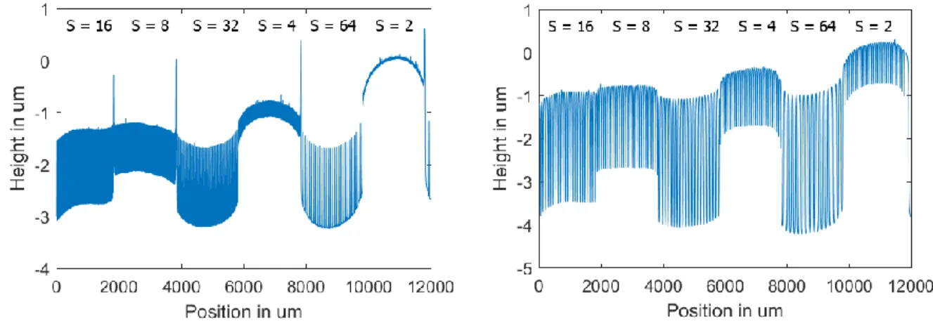
As previously described, each TV consists of a matrix of uniform regions of parallel lines. While each uniform region could be individually profiled, instead multiple uniform regions are profiled in a single scan. This allows both the feature scale variations, as well as the transitions between uniform regions, to be measured. As only the upper half of the TV is profiled, the line width within each scan is constant, while the line spacings change within each scan. Between scans, the line width changes, while the ordering of the spacings is constant. The ordering of the spacings in each scan is 16 µm, 8 µm, 32 µm, 4 µm, 64 µm, 2 µm. Sample scans can be seen in Fig. 10, while a complete collection of the scans for all combinations of line widths, spacings, heights, and polyimide thicknesses are presented in the appendix alongside their model predictions.
Figure 10: Sample experimental profiles for W = 4 𝜇𝑚 (left) and W = 64 𝜇𝑚 (right). Both are from the H =5 𝜇𝑚, T = 8 𝜇𝑚 TV.
2.2.1) Feature Scale Variation
After profiling each TV, the scans are analyzed. A key statistic extracted is the feature scale variation. The feature scale variation is defined as the average difference between the peak and the troughs within a given uniform region and is found to be a function of line width, spacing, height, and polyimide thickness. To calculate this value, only the middle third of each uniform region is analyzed. This minimizes the impact of the adjacent uniform regions. This middle third is then divided into smaller segments of length 𝑊 + 𝑆 (the pitch of the uniform region in the TV), and the minimum and maximum value are extracted from each period. Finally the differences between
23 these minima and maxima is averaged over all periods for each uniform region to find the average feature scale variation.
While the feature scale variation is a function of both line width and spacing, these two variables can be simplified into a new parameter defined as the effective feature width, 𝑊𝑒𝑓𝑓:
𝑊𝑒𝑓𝑓 =𝑊+𝑆𝑊∙𝑆.
All combinations of widths and spacings with equivalent 𝑊𝑒𝑓𝑓 will have equal feature scale
variations. This value represents the variation due to an isolated feature with width 𝑊𝑒𝑓𝑓. As 𝑆
approaches ∞, the feature becomes isolated, and 𝑊𝑒𝑓𝑓simplifies to 𝑊, the width of the feature. A similar analysis shows that this is also the variation due to an isolated trench of “spacing” 𝑆. It should be noted that 𝑊𝑒𝑓𝑓 ≤ 𝑊, 𝑆 for all combinations of 𝑊 and 𝑆. After later developing the spin
coating model, the development of this simplification is expanded upon in Section 3.8.
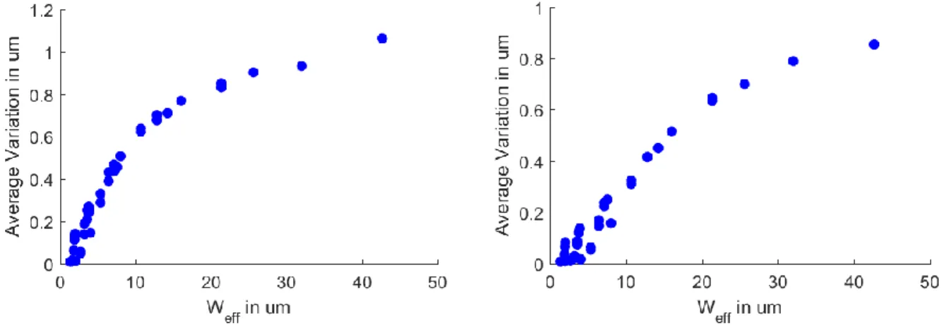
The variation in each uniform region as a function of 𝑊𝑒𝑓𝑓 can be seen in Fig. 11 for H =
2 µm with T = 8 µm and for H = 2 µm with T =13 µm. The variations for the remainder of the coated TVs can be seen in the appendix next to the corresponding model predictions.
Figure 11: Feature scale variations vs. 𝑤𝑒𝑓𝑓 for H = 2 𝜇𝑚 with T = 8 𝜇𝑚 (left), and 13 𝜇𝑚 (right).
2.2.2) Long Range Variation
In addition to calculating the feature scale variations for each region, the long range, or chip scale, effects of the underlying topography are also considered. Here, a complete 2D profile for the coated TV is constructed, then the average heights within the uniform regions are calculated. To build this 2D profile, the previous profile scans, similar to those of Fig. 12, are
24 combined with a single column scan of the TV. This single column scan determines the relative heights between the row measurements, thus allowing the relative heights between all profiled regions to be known. It should be noted that the column measurement is taken from the S = 2 µm column. This is the column with the lowest feature scale variation, thus minimizing the uncertainty of the 2D profile. Fig. 13 shows the location of each measurement, while Fig. 14 shows the complete TV profile.
Figure 12: Example scan of a TV Row.
Figure 13: Illustration of scan locations: row scans (left), column scan (center), and complete scans (right).
25 The average height of each uniform region is calculated to quantify these chip scale variations. It is found that the height variation between uniform regions is approximately linear with pattern density (𝑊+𝑆𝑊 ). Intuitively this makes sense, and suggests a conservation of mass during spin coating. Each uniform region contains the same amount of polyimide; however, its distribution within the region may differ based on the underlying topography. Therefore, the relative average height after spin coating is the same as the relative average height before spin coating, 𝐻 ∙𝑊+𝑆𝑊 . Plots for the average height of each uniform region for H = 1.8 and 4.2 um and
T = 8, and 11 um, can be seen in Fig. 15.
Figure 15: Averge heights as a function of pattern density. H = 1.8 um (top), H = 4.2 um (bottom), T = 8 um (left), T = 11 um (right).
2.2.3) Tip Pinch-Off and Measurement Fidelity
For high aspect ratio trenches, tip pinch off during profilometry scans was encountered. As the line height increases, the stylus tip no longer reaches the bottom of the high aspect ratio
26 trenches as illustrated in Fig. 16.
Figure 16: Tip pinch off for high aspect ratio trench.
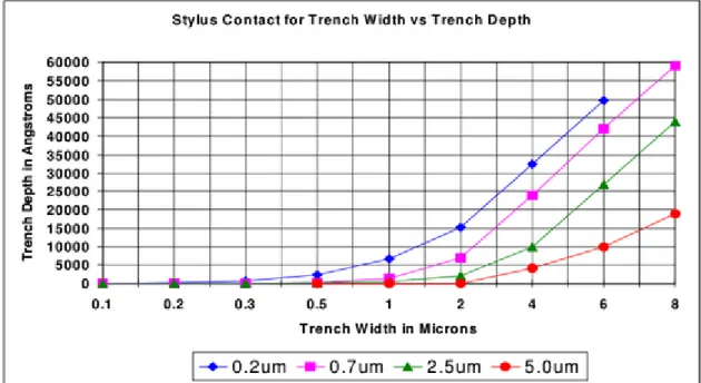
This was first noticed while developing an initial version of the model that systematically overpredicted the feature scale variation when compared to the experimental results. It was then noticed that the effective feature width simplification would also break down for high aspect ratio trenches. These two phenomenon suggested that tip pinch off was occurring. The original tip radius used was 12.5 µm, but after purchasing a new tip of radius 2 µm, both of these problems were resolved. The tip manufacturer, Bruker Corporation, provides the maximum trench depth possible to resolve given the trench width for common tip radii, which can be seen in Fig. 17. For 8 µm spacings, all of the trench feature scale variations are measured to be smaller than 4 µm, and for 4 µm spacings, all feature scale variations are under 1.5 µm, except one (line height 9 µm, polyimide thickness 8 µm). As the tip radii is 2 µm, these should all be under the maximum resolvable trench depth.
Figure 17: Maximum resolvable trench depth as a function of trench width and stylus radius [Bruker Nano Inc., personal communication, April 21, 2016].
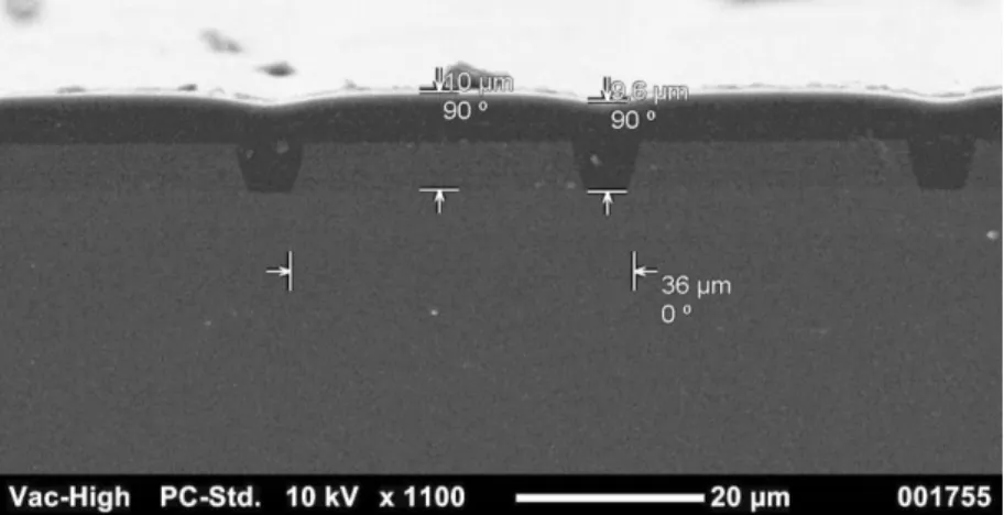
27 To confirm this, cross sectional images are taken and compared to the profilometry results. SEM images for a coated TV of line height of 5 µm, line width of 32 µm, polyimide thickness of 8 µm and spacings of 2 µm and 4 µm are shown in Figs. 18 and 19.
Figure 18: Cross sectional SEM image of H = 5 µm , T = 8 µm , W = 32 µm, S = 2 µm.
Figure 19: Cross sectional SEM image of H = 5 µm , T = 8 µm , W = 32 µm, S = 2 µm.
The feature scale variations measured using the SEM images are compared to those of the profilometer, and are presented in Fig. 20. The variation measured by the SEM is consistently lower than that of the profilometer, especially for small spacings. This suggests that the profilometry scans are not suffering from pinch off, otherwise the SEM scans would give consistently larger variations. This discrepancy is most likely due to the truncation of the SEM measurements. Distances measured using the SEM are truncated at two significant figures, and therefore the peak measurements are all 10 µm (as opposed to 10.5 µm, for example). This lowers the variation measured by the SEM.
28
Figure 20: Surface variation measured using SEM vs. Profilometer for H = 5 µm, T = 8 µm.
Using the 2 µm profilometer tip, the effective feature width simplification works well. If the profilometry scans were to still suffer from pinch off, they would produce smaller variations for small spacings and large line widths compared to the variation from large spacings and small line widths. The fact that this is not the case provides the final piece of evidence to confirm that the profilometry scans accurately represent the true coated profiles.
29
Chapter 3: Modeling
In this chapter, the predictive model for the spin coated surfaces is developed. At a high level, the coated profile is modeled as a convolution between the underlying topography and an appropriately chosen impulse response. This modeling technique has been used for similar pattern dependent processes [19, 20].
After presenting the model form in Section 3.1, the impulse response for each coated TV is experimentally determined in Section 3.2. Then, the experimental data is fit to an analytic form, and the surface of the coated TV is predicted and presented in Section 3.3. These predictions are then compared to the experimental data in Section 3.4, and an optional addition to the model is presented in Section 3.5 that improves the accuracy for extremal cases. The trends seen in the model coefficients and a closed form analysis are then discussed in Sections 3.6 through Section 3.8. We revisit the existing models and compare them to the one presented in this thesis in Sections 3.9 through 3.11. Finally, the model is expanded to two dimensions, and the coating of non-binary and two-dimensional surfaces are predicted in Sections 3.12 through 3.14.
3.1) Model Form
As mentioned, the coated surface is modeled as a convolution between an appropriately chosen impulse response and the starting topography. From a signal processing perspective, the input signal is the underlying profile, 𝑝𝑢(𝑥), the output is the coated profile, 𝑝𝑐(𝑥), and the system
represents the act of coating the wafer, with an impulse response ℎ(𝑥). 𝑝𝑐(𝑥) = ∫ 𝑝𝑢(𝑥 − 𝑥′) ∙ ℎ(𝑥′) 𝑑𝑥′
= 𝑝𝑢(𝑥) ∗ ℎ(𝑥)
Here, the convention used is that the reference height for 𝑝𝑐(𝑥) is the coated, but
un-patterned, area. To find the height above the silicon wafer surface, the thicknesses of each polyimide layer on a flat surface must also be added.
3.2) System Impulse, Step, and Frequency Response
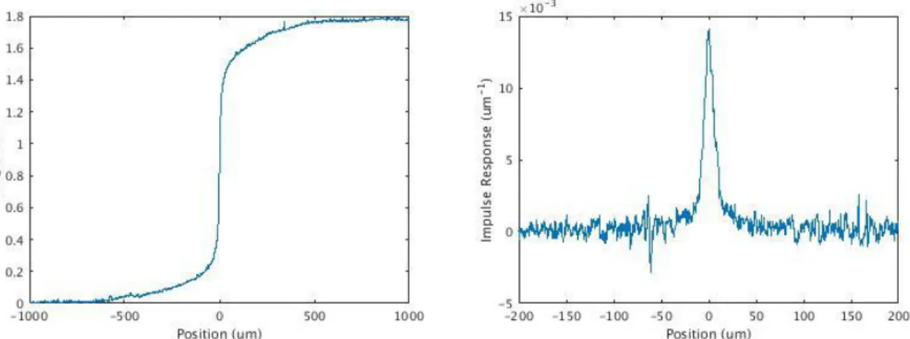
The impulse response of the system cannot be directly measured, but can instead be derived from the step response, 𝐸(𝑥), of the system. As the model takes the form of an LTI system, the
30 impulse response is derived by taking the derivative of the step response, as shown in Fig. 21. These step responses are obtained by measuring the profile of a coated “step” in height on the TV. Here, 𝑝𝑢(𝑥) = 1 for 𝑥 ≥ 0 and 𝑝𝑢(𝑥) = 0 for 𝑥 < 0.
When measuring this step response, it is best to measure a step which is as isolated as possible. This reduces the effects that surrounding regions have on the step response. In practice, the steps measured are at least 2000 µm away from any other feature, and the responses were truncated 1000 µm away from the feature itself.
Figure 21: Example unprocessed step response (left), and derived impulse response (right).
To reduce noise in the measurements, six step responses are averaged for each line height and polyimide thickness combination. Here, the peaks of each impulse response are used to align the step responses. Two of these step responses are measured 1 cm away from the center of the wafer, two 3 cm away, and two 5 cm away. It should be noted that later in Section 3.10, the impulse response is shown to be independent of the radial distance from the center of the wafer, allowing the responses to be averaged at multiple locations. Finally, the step responses are leveled in post processing by setting the slopes of the responses at each edge to be zero. This is done by fitting the first and last 10% of each step response to a first order polynomial, and subtracting the average of these two fits from the experimental data.
3.2.1) Initial Fit
After experimentally collecting the step and impulse responses, they are fit to an analytic function. While the form of the impulse response is not immediately obvious, its Fourier Transform, the spatial system frequency response, is easier to observe. As shown below, the spatial
31 frequency response of the system fits nicely to the form:
ℋ(𝑘) = 𝑒−𝛽|𝑘|
where k is the spatial frequency, and β is a constant that encapsulates the system parameters. Sample system response fits using this form are shown in Fig. 22.
Figure 22: System spatial frequency response fit to 𝑒−𝛽|𝑘|. H = 1.8 um (top), H = 4.2 um (bottom), T = 8 um (left), T = 13 um (right).
Using the inverse Fourier Transform, the impulse response takes the form:
ℎ(𝑥) = 𝛽
𝜋 ∙ (𝛽2+ 𝑥2)
Fig. 23 shows the fits for the experimental impulse responses. Finally, integrating ℎ(𝑥) with respect to x gives the form of the normalized step response:
𝐸(𝑥) = tan −1(𝑥 𝛽) 𝜋 + 1 2
32 This agrees with intuitive expectation for the systems step response. Near the feature there is a steep slope, and further away, the height asymptotically approaches either 0 or 1.
Figure 23: Impulse responses fit to 𝜋∙(𝛽𝛽2+𝑥2). H = 1.8 um (top), H = 4.2 um (bottom), T = 8 um (left), T = 13 um (right).
While the frequency response fits nicely to its proposed form, a discrepancy exists near 𝑘 = 0. By definition, ℋ(0) = 1, as the impulse response must integrate to 1. However, the fit does not intersect with this point. Instead there appears to be an impulse at 𝑘 = 0. If this is real, the new frequency response takes the form:
ℋ(𝑘) = 𝑒−𝛽 |𝑘|+ 𝑐 𝛿(𝑘)
33 ℎ(𝑥) = 𝛽 𝜋 (𝛽2+ 𝑥2)+ 𝑐 and: 𝐸(𝑥) = tan −1(𝑥 𝛽) 𝜋 + 1 2 + c x
This corresponds to a constant offset in the impulse response, and therefore an additional constant slope in the step response. This implies that infinitely far away from a feature, the coating thickness is infinite, which does not make intuitive sense. Instead, the zero frequency offset is attributed to a leveling and scaling issue during the step response measurements.
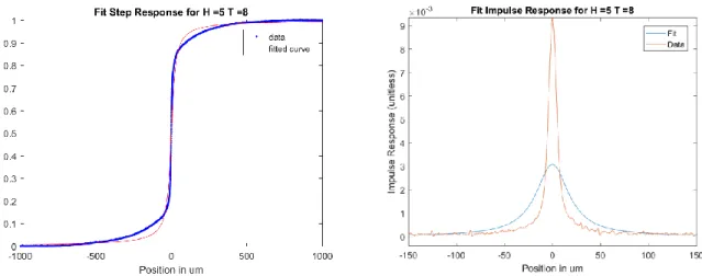
3.2.2) Updated Fit
While this form fits the impulse response well, the corresponding step response fit is less accurate than desired. A sample fit for the step response, as well as the resulting impulse response fit can be seen in Fig. 24. Here, fitting the model to the impulse response results in a different fit than fitting the model to the step response. In the first case, the mean squared error (MSE) of the impulse response fit is minimized, while in the second case the MSE of the integral of the impulse response fit is minimized. These are two separate optimization problems with different answers, explaining why the impulse response fit looks poor when the step response fit is optimized and vice-versa.
34
corresponding impulse response fit using original form.
Clearly, fitting the step response to the hypothesized model does not produce the most accurate results for the corresponding impulse response. While this fit does capture the coating shape immediately near the feature, its accuracy quickly degrades as the distance from the feature increases. Therefore, when using this form of the model, the long range, or chip scale, effects are typically lost when predicting coated profiles. This phenomenon is further explored in Section 3.7 after presenting the results of the updated model.
The error between the step fit and experimental profile is presented in Fig. 25. Here, the error on each side of the feature can be approximated as a decaying exponential. To improve our model, this term is added to the system response fit to account for this error.
Figure 25: Step response error using original form.
When this term is added, the new impulse response takes the form:
ℎ(𝑥) = 𝑎 ∙ 𝑏
𝜋 ∙ (𝑏2+ 𝑥2)+ (1 − 𝑎) ∙ 𝑒− |𝑥|
𝑐 ∙ 1
2 ∙ 𝑐 And the step response takes the form:
𝐸(𝑥) = 𝑎 ∙ ( atan( 𝑥 𝑏) 𝜋 + 1 2 ) + (1 − 𝑎) ∙ 𝑒 𝑥 𝑐∙1 2 for 𝑥 ≤ 0
35 𝐸(𝑥) = 𝑎 ∙ ( atan( 𝑥 𝑏) 𝜋 + 1 2 ) + (1 − 𝑎) ∙ (1 − 𝑒 −𝑥 𝑐 ∙1 2) for 𝑥 ≥ 0
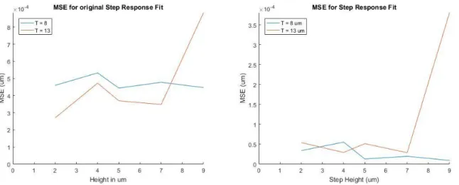
Here, 𝑏 is analogous to 𝛽 in the original model, 𝑐 represents the decay constant of the exponential term, and 𝑎 is the weighting between the two terms. Using this updated model, the fit of both the step response and its corresponding impulse response is much closer to the experimental results. In Fig. 26, the mean squared error is plotted for the original and updated step response fit. Averaged across all combinations of H and T, the MSE for the updated fit is 6.75 ∙ 10−5 𝑢𝑚, 11.82% of that
of the original MSE.
Figure 26: Mean squared error of step response fit using original (left) and updated (right) form.
In this updated model, the first term captures the impact of coating very close the feature, giving a good fit to the impulse response and to the feature scale variations, while the second term captures the impact of coating far away from the feature, improving the step response fit and capturing the longer range process effects, such as the transitions between uniform regions. The significance of these two terms is later explored in Section 3.7 after first discussing the results of the model Section 3.4.
36
Figure 27: Impulse and step response fits using model update.
3.3) Model Predictions
After developing the process model and fitting it to the measured step responses, the coated TV profiles are predicted. For each coated TV, the same profiles as shown in Section 2.2 are predicted. Sample coating predictions compared to their corresponding experimental scans can be seen in Fig. 28, and sample feature scale variation predictions compared to their corresponding experimental results can be seen in Fig. 29. The remainder of the predicted coatings, predicted feature scale variations, and both sets of experimental results can be seen in the appendix.
37
Figure 28: Experimental (left) and predicted (right) scans for H = 5 um, T = 8 um, W = 4 um (top), W = 64 um (bottom).
38
Figure 29: Experimental (left) and predicted (right) feature scale variations for H = 4 um, T = 8 um (top), T = 13 um(bottom).
3.4) Model Accuracy
Ideally, the accuracy of the model would be quantified on a point-by-point basis, using either the mean-squared error or cross correlation value, but in practice, this is difficult. The first difficulty arises from the fact that the experimental scans are not level. Adding slopes to the experimental scans creates large differences between the two sets of scans, giving the model deceptively poor accuracy. A second problem with this approach comes from the angular offset between the two scans. The predicted scans are theoretical, and are perfectly perpendicular to the underlying lines; however, this is not true for the experimental scans. Due to this angular offset, the experimental scans are slightly stretched, as these scans must be longer to cover the same number of underlying lines. While both of these problems could be corrected for using optimization techniques, a simpler method is used to quantify the accuracy.
39 Instead, the models accuracy is assessed by comparing the predicted and experimental feature scale variations as defined in Section 2.2.1. For each combination of line width, spacing, height and polyimide thickness, the error is calculated by taking the difference between the predicted and experimental variations and normalizing by the line height.
The resulting assessment of the models accuracy for all combinations of line width, spacing, height, and polyimide thickness are shown in Fig. 30. The mean error for these predictions is 4.4%, and the standard deviation is 0.043. Additionally the maximum prediction error is 23.5%. This is a surprisingly high maximum prediction error, and exposes a limitation of the model. The model consistently under-predicts the variation for lines with small width and large spacings. However, this is only the case for large line heights and small polyimide thicknesses, and these extremal cases are relatively uncommon in RDLs.
H (um)
T = 8
T = 13
2
40
5
7
9
Figure 30: Feature scale errors for all coated TVs.
3.5) Model Extremal Cases
To analyze the source of this error, consider a thin, isolated, interconnect, whose height (H) is larger than the polyimide thickness on a flat surface (T). Here, the copper line will be poking through the polyimide surface. Clearly, the surface variation cannot be less than the difference between the height of the interconnect and the polyimide thickness. However, by making the interconnect arbitrarily narrow, the model will predict an arbitrarily small surface variation. The
41 predicted coated profile will be:
𝑝𝑐(𝑥) = ∫ 𝑝𝑢(𝑥 − 𝑥′) ∙ ℎ(𝑥′) 𝑑𝑥′
= ∫ 1 ∙ ℎ(𝑥Δ ′)𝑑𝑥 −Δ
= 0 for all 𝑥 as Δ → 0
Where ℎ(𝑥) is the impulse response, 𝑝𝑐 is the coated profile, and 𝑝𝑢 is the underlying profile whose height is 1 between – Δ and Δ and 0 elsewhere.
While this seems like a major limitation of the model, in practice, it is an unlikely extremal case. In order for this error to be significant, three conditions must be simultaneously met:
1) The line height must be larger than the line width.
2) The line height must be larger than the polyimide thickness.
3) The spacing of the lines must be significantly larger than the width of the lines (~2x). The first condition is required for the model to predict approximately zero surface variation, as the width of the feature must be small. The second condition must be met in order for the lines to rise above the flat polyimide surface. While the error occurs when T = 8 µm, it is unseen when T = 13 µm. Additionally, while the nominal thickness is 8 µm for the thinner polyimide, the cross sectional SEM images in Figs. 18 and 19 show that the real value is closer to 6.5 µm, exacerbating this effect. Finally, the third requirement is necessary as lines with small spacing and line width do not show this error under any conditions.
3.5.1) Penalty Function for Extremal Cases
While these extremal cases are relatively uncommon in typical RDL applications, we propose a simple addition to the model that can improve predictions in these extremal cases and leave correct predictions unaffected. This improvement is not typically necessary for predicting surface variations in RDLs, however, it may be useful for alternative spin coating applications.
This correction to the model is applied after the standard predictions are made, and attempts to compensate for the extremal cases similar to those of Section 3.5. After predicting the surface using the standard model, we define the uncompensated dielectric thickness, 𝑟(𝑥), at each point:
42 𝑟(𝑥) = 𝑝𝑐(𝑥) − 𝑝𝑢(𝑥)
This is the distance from the underlying topography to the predicted surface. If this value is less than 0, then our model has predicted a negative dielectric thickness, and we know that our model has under-predicted the coated surface.
We then compute a penalty function 𝑓𝑝(𝑟), and add this back to the prediction in order to
compensate:
𝑝𝑐 = 𝑝𝑐+ 𝑓𝑝(𝑟)
There are many option for choosing the correct form of 𝑓𝑝(𝑟), but all viable forms must meet two requirements. First, 𝑝𝑐(𝑥) > 𝑝𝑢(𝑥) for all 𝑥. This corresponds to the physical constraint
of having the predicted coating be higher than the underlying topography. Secondly, if 𝑝𝑐(𝑥) ≫ 𝑝𝑢(𝑥) then 𝑓𝑝(𝑟) ≈ 0. This correspond to cases where the predicted coating is significantly higher than the underlying topography, as in regimes where the model already accurately predicts the surface. Therefore, these cases should remain unaffected by 𝑓𝑝(𝑟).
While the optimal form of 𝑓𝑝(𝑟) is not known, we propose a form which meets all of these
requirements, and is successful in compensating for the extremal cases: 𝑓𝑝(𝑟) = 𝑦𝑎𝑛𝑐ℎ∙ 𝑒−
(𝑟−𝑥𝑎𝑛𝑐ℎ)2
𝑑
The terms 𝑥𝑎𝑛𝑐ℎand 𝑦𝑎𝑛𝑐ℎ are “anchor points” where the value of 𝑓𝑝(𝑟) is approximately known. By choosing these points, we set 𝑓𝑝(𝑥𝑎𝑛𝑐ℎ) = 𝑦𝑎𝑛𝑐ℎ. To determine both values, consider
two cases.
First, consider the case when 𝐻 ≫ 𝑇. Here, the prediction is flat, but the underlying topography “pokes out” through our prediction, as illustrated in Fig. 31. In this case, we can assign 𝑥𝑎𝑛𝑐ℎ = 𝑇 − 𝐻, and 𝑦𝑎𝑛𝑐ℎ = 𝐻 − 𝑇. By setting this, we ensure that when 𝑟 ≈ 𝑇 − 𝐻 and the line pokes through the surface, our prediction is compensated by this distance, ensuring that 𝑝𝑐(𝑥) > 𝑝𝑢(𝑥).
43
Figure 31: Narrow, isolated line (green) when H >> T (polyimide is in blue).
Second, consider the case when 𝐻 ≪ 𝑇. Here, our predictions are always significantly higher than the underlying topography. In these cases, our unmodified model is correct, and thus we do not want to make significant changes. We can again set 𝑥𝑎𝑛𝑐ℎ= 𝑇 − 𝐻, but this time
set 𝑦𝑎𝑛𝑐ℎ= 0. By doing this, we ensure that 𝑓𝑝(𝑟) = 0 for all 𝑟, and our correct predictions are
not altered.
We can then combine these two cases by always setting 𝑥𝑎𝑛𝑐ℎ = 𝑇 − 𝐻, and could use 𝑦𝑎𝑛𝑐ℎ = max (0, 𝐻 − 𝑇). In order to use a smooth function for computing 𝑦𝑎𝑛𝑐ℎ, we can
instead use a smooth maximum:
𝑦𝑎𝑛𝑐ℎ = log (1 + 𝑒𝐻−𝑇)
By choosing these points, we set 𝑥𝑎𝑛𝑐ℎ as the minimum uncompensated dielectric thickness possible. Because the predicted surface cannot be lower than 𝑇, and the underlying topography cannot be higher than 𝐻, the uncompensated thickness cannot be smaller than 𝑇 − 𝐻. Therefore, this penalty function will have a maximum value of 𝑦𝑎𝑛𝑐ℎ ≈ max (0, 𝐻 − 𝑇) in the worst case prediction (the flat prediction with an infinitely narrow interconnect analyzed in the previous section). Additionally, the impact of 𝑓𝑝(𝑟) will diminish as the uncompensated dielectric thickness increases, and as the original model becomes more accurate.
The final choice in determining 𝑓𝑝(𝑟) is then to determine the decay constant 𝑑. Here, we select a value which minimizes the MSE between the prediction and measurements over a complex topography. We optimize over all TVs used, and select the value 𝑑 = 25 𝜇𝑚2. While it is likely
the case that each set of process parameters should have its own corresponding value of 𝑑, we did not find it necessary to optimize 𝑑 separately for each coated TV to show the effectiveness of the
44 penalty function.
By using this version of 𝑓𝑝(𝑟), we reduce the max feature scale error over all TV’s from
23.5% to 12% of the line height, and the average error from 4.4% to 3.5%. This is a significant improvement, especially in the extremal cases where the unmodified version breaks down. In Fig. 32, we present three sets of scans that each show the experimental, unmodified, and modified predictions. Example 1 shows the profiles for 𝐻 = 9 𝜇𝑚, 𝑇 = 8 𝜇𝑚 and 𝑊 = 4 𝜇𝑚. Example 2 shows the profiles for 𝐻 = 7 𝜇𝑚, 𝑇 = 8 𝜇𝑚 and 𝑊 = 4 𝜇𝑚. Example 3 shows the profiles for 𝐻 = 5 𝜇𝑚, 𝑇 = 13 𝜇𝑚 and 𝑊 = 16 𝜇𝑚. Two of the three scans show an improvement, while the third shows a relatively correct and unmodified prediction.
Example
Experimental
Prior
Modified
1
2
3
Figure 32: Experimental, prior, and modified scans using penalty function. First two (1,2) show desired change, and the Third (already correct) remains unaffected.
Additionally, we can see the improvement in the accuracy from error plots first shown in Section 3.4. In particular, the cases of 𝑇 = 8 𝜇𝑚 and 𝐻 = 7 or 9 𝜇𝑚 show significant
45 improvement. In Fig. 33, we include both the previous errors, and the errors after implementing the penalty function. We note that for all other cases, the errors were not significantly affected as 𝐻 < 𝑇 for these cases.
Previous
Updated
T = 8,
H = 7
T = 8,
H = 9
Figure 33: Uncompensated (left) and corrected (right) feature scale errors for T = 8 µm with H = 7 µm (top), and T =8 µm with H = 9 µm (bottom).
While the inclusion of the penalty function does improve the extremal cases, we note that its inclusion is not required, and for the remainder of this thesis, we will ignore it for simplicity. Finally, we note that while the form of 𝑓𝑝(𝑟) does improve results, our proposed form is likely
sub-optimal, and further improvements to its form can be made.
3.6) Model Trends
The 𝑎, 𝑏, and 𝑐 coefficients present in our modeled system responses empirically encapsulates the effects of all spin coating parameters, including line height, coating thickness, spin speed, and the material properties of the polyimide. The measured coefficients as a function of coating thickness and step height can be seen below in Fig. 34.
46 the optimum polyimide, line height and spin speed could be selected to minimize surface variation while meeting other design criteria. Unfortunately, the extracted parameters do not show any clear trends from which an empirical model can be developed that would predict the model coefficients from material and procedural constants.
While we cannot quantitatively predict the change, we believe that increasing the coating thickness will increase the 𝑏 coefficient, as this effect is seen in all cases where the line height is kept constant. This increase in 𝑏 leads to a more planar coated surface, as the step response term atan (𝑥𝑏) will be stretched horizontally. Intuitively this makes sense, as increasing the polyimide thickness should smooth out the underlying topography more heavily.
Besides this, there are no other clear trends in the model coefficients. While 𝑏 appears to decrease with line height for 𝑇 = 8 µm, it is constant with line height for 𝑇 = 13 µm. Additionally, both 𝑎 and 𝑐 seem to be constant with both line height and coating thickness; however, there is not enough data to fully confirm this. We believe that the lack of clear coefficient trends is likely due to differences in the curing procedure between TVs. This effect is later revisited and explained in Section 3.11.
Figure 34: a, b, and c coefficients as a function of line height for T = 1.8 um (blue), and 13 um (red).
3.7) Impact of Updated Fit and Coefficient Significance
47 updated to include an additional term to address long-range variation effects. Now, the significance of this update and of the model terms is investigated. First, sample predictions using the original model are shown and compared to their updated versions. Then the impact of both system response terms is analytically examined both near the feature, and far away from the feature. Together, the predictions and the closed form analysis will give intuition for each model term.
In the original model, the impulse response takes the form:
ℎ(𝑥) = 𝑏
𝜋 (𝑏2+ 𝑥2)
While this fits well near the feature itself, its accuracy commonly degrades outside of this small range as can be seen in Fig. 35.
Figure 35: Impulse response showing good fit near center, while the accuracy degrades further away.
Using the simpler version of the model, the predictions lack many of the long range effects present in both the experimental scans, and the predictions using the updated fit. Fig. 36 shows four profiles that highlight the importance of the model update. Fig. 36a shows the experimental scan; Fig. 36b shows the prediction using the original impulse response fit; Fig. 36c shows the prediction using the updated impulse response fit; finally, Fig. 36d shows the prediction using the experimental impulse response. In this case the raw, unfit impulse response is used during the
48 convolution. For all figures, H = 5 µm, T = 13 µm, and W = 32 µm. The spacings change within each graph, and are 16 µm, 8 µm, 32 µm, 4 µm, 64 µm, and 2 µm in that order.
Figure 36: Sample experimental scan (upper left), prediction using original form (upper right), prediction using updated form (lower left), prediction
using experimental impulse response (lower right).
In all profiles, the feature scale variations within each region are approximately the same. The most significant difference between these profiles is that the profile predicted using the original fit lacks the gradual transitions between uniform regions. This signifies that the 𝜋(𝑏2𝑏+𝑥2) term captures the feature scale variations, while the 𝑒−|𝑥|𝑐 ∙ 1
2∗𝑐 term captures the long range, or chip
49 Now, the effect of each term is analytically examined near the feature and far away from the feature in order to show the impact of each. Here, it is assumed that 𝑏 ≪ 𝑐, as this is the case in all observed fits. At the feature itself (𝑥 = 0), the feature scale term has a value 𝜋(𝑏2𝑏+02)=𝜋 𝑏1 , and the long range term has a value 𝑒−|0|𝑐 ∙ 1
2∗𝑐 =
1
2 𝑐. As 𝑏 ≪ 𝑐, it is clear that the feature scale term
dominates near 𝑥 = 0. Additionally, when 𝑥 ≈ 𝑐, relatively far away from the feature, the feature scale term has a value 𝜋(𝑏2𝑏+𝑐2)≈𝑐𝑏2, and the long range term has a value 𝑒−|𝑐|𝑐 ∙ 1
2∙𝑐 ≈
1
𝑐. In this
case, 𝑏 ≪ 𝑐, thus 𝑐𝑏2 ≪1𝑐, and in this case the long range term dominates. This analysis demonstrates why the original model can predict the feature scale variations, while it was unable to predict the gradual transitions between regions.
Finally, it is also worth noting that the profiles using the updated fit and experimental impulse responses are almost identical. This is expected, as the MSE between the two step responses is 6.75 ∙ 10−5 𝑢𝑚. Therefore, the impulse responses and predicted profiles are similarly
close, and further updates to the fit are not necessary.
However, the similarity between the predictions using the updated fit and those using experimental data raises an interesting question: Why is fitting necessary if using the experimental impulse response results in a similarly accurate prediction? The answer to this is twofold. First, by fitting the data to a compact model, the amount of information needed to quantify the process is greatly reduced. Using the fit, only three values are needed to quantify the system, one for each of the model coefficients. However, using the experimental data, a value for every sampled point would be needed. Therefore, the model fit provides a convenient way to compare which process will result in more planar structures. Secondly, by fitting the impulse responses, the noise from the experimental data is reduced. This will be important when the model is expanded to two dimensions and 2D impulse responses are generated from the 1D responses. The algorithm used for this has a low noise tolerance and will be expanded upon in Section 3.14.
3.8) Closed Form Analysis
Here, closed form results are developed for regions with uniform line height, spacing, and width. This will explain the effective feature size approximation first introduced in Section 2.2.1,
50 and will help establish design rule guidelines which will later be expanded upon in Chapter 4. In this analysis, only relatively small feature sizes are considered, particularly those where 𝑤, 𝑠 ≪ 𝑐, the coefficient related to the long range variations.
To approach this problem, first consider the coating over an individual feature as shown in Fig. 37.
Figure 37: Ideal coating over an isolated interconnect.
To find the variation in the coated profile, 𝑝𝑐, the minimum and maximum heights of the coated profile, 𝑃𝑚𝑖𝑛 and 𝑃𝑚𝑎𝑥, must be determined. The minimum height of the coated profile occurs infinitely far away from the feature, and 𝑇 µm above the wafer surface. Using the original convention, this point has an absolute height of zero. Additionally, 𝑥 = 0 is the point where 𝑝𝑐(𝑥) = 𝑃𝑚𝑎𝑥.
Because the model takes the form of a LTI system, the underlying profile, 𝑝𝑢(𝑥), can be separated into two parts, a step up, followed by a step down. Then, the resulting profiles can be summed to find 𝑝𝑐(𝑥). Here, 𝑢(𝑥) refers to the Heaviside (step) function.
𝑝𝑢(𝑥) = 𝐻 ∙ (𝑢 (𝑥 +𝑤
2) − 𝑢 (𝑥 − 𝑤
2)) Then, using the closed form step responses:
51 𝑃𝑚𝑎𝑥 = 𝑝𝑐(0) = 𝐻 ∙ (𝑎 ∙atan ( 𝑤 2 𝑏) 𝜋 − 𝑎 ∙ atan (−2 𝑏)𝑤 𝜋 − +(1 − 𝑎) ∙ (1 − 𝑒 −𝑤 2𝑐 ∙1 2) − (1 − 𝑎) ∙ 𝑒 𝑤 2𝑐∙1 2 ) Because 𝑥 ≪ 𝑐, this can be approximated by:
𝑃𝑚𝑎𝑥 ≈ 𝐻 ∙ (𝑎 ∙atan ( 𝑤 2 𝑏) 𝜋 − 𝑎 ∙ atan (−2 𝑏)𝑤 𝜋 )
Finally, as atan(𝑥) is an odd function, atan(−𝑥) = − atan(𝑥) and: 𝑃𝑚𝑎𝑥 = 2 ∙ 𝐻 ∙ 𝑎
𝜋 atan ( 𝑤 2 𝑏)
This gives a closed form solution to the variation from a single feature with 𝑤 ≪ 𝑐. In Fig. 38, this approximation is plotted against the experimental variations as a function of 𝑊𝑒𝑓𝑓 for 𝐻 =
4 𝜇𝑚, and 𝑇 = 13 𝜇𝑚. As previously described, 𝑊𝑒𝑓𝑓 =𝑤+𝑠𝑤∙𝑠 and is the effective width for a given line width and spacing. Here, the variation from a uniform region of lines with width 𝑤 and spacing 𝑠 should match the variation caused by an isolated feature of width 𝑊𝑒𝑓𝑓.
Figure 38: Closed form approximation for feature scale variation vs. 𝑤𝑒𝑓𝑓.
52 similar to those in the TV, as illustrated schematically in Fig. 39.
Figure 39: Ideal coating over an infinite array of lines.
Again, the feature scale variation is found by taking the difference between 𝑃𝑚𝑖𝑛 and 𝑃𝑚𝑎𝑥.
First, the starting profile is broken apart into individual steps:
𝑝𝑢(𝑥) = 𝐻 ∑ 𝑢 (𝑥 +𝑤2 + 𝑖 ∙ (𝑤 + 𝑠)) − 𝑢 (𝑥 −𝑤
2 + 𝑖 ∙ (𝑤 + 𝑠))
∞
𝑖 = −∞
The simplification 𝑤 ≪ 𝑐 is again used to approximate the coated profile: 𝑝𝑐(𝑥) ≈ 𝐻 ∙ 𝑎 𝜋 ∑ atan ( 𝑥 +𝑤2 + 𝑖 ∙ (𝑤 + 𝑠) b ) − atan ( 𝑥 −𝑤2 + 𝑖 ∙ (𝑤 + 𝑠) b ) ∞ 𝑖 = −∞
Again, 𝑃𝑚𝑎𝑥 occurs directly above the feature at 𝑥 = 0, but now 𝑃𝑚𝑖𝑛 occurs in the spaces
between features, at 𝑥 =𝑤+𝑠2 : 𝑃𝑚𝑎𝑥 = 𝐻 ∙ 𝑎 𝜋 ∑ atan ( 𝑤 2 + 𝑖 ∙ (𝑤 + 𝑠) b ) − atan ( −𝑤2 + 𝑖 ∙ (𝑤 + 𝑠) b ) ∞ 𝑖 = −∞ 𝑃𝑚𝑖𝑛 = 𝐻 ∙ 𝑎 𝜋 ∑ atan ( −𝑠2 + 𝑖 ∙ (𝑤 + 𝑠) b ) − atan ( 𝑠 2 + 𝑖 ∙ (𝑤 + 𝑠) b ) ∞ 𝑖 = −∞