Advanced Filters and Components for Power
Applications
by
Timothy C. Neugebauer
B.S., Union College (1997)S.M., Massachusetts Institute of Technology (1999)
Submitted to the Department of Electrical Engineering and Computer Science in partial fulfillment of the requirements for the degree of
Doctor of Philosophy
at theMASSACHUSETTS INSTITUTE OF TECHNOLOGY
June 2004
@
Massachusetts Institute of Technology, MMIV. All rights reserved.Author_
Depa t nt of EleC5a1 Engineering and Computer Science
May 19, 2004
Certified
by-Assistant Professor pf--El66trical ngineering
David J. Perreault a-nTi~Cmputer Science "Thesis upervisor Accepted by MASSACHUSETTS INST]TUTE OF TECHNOLOGY
JUL 2
6
2004
Arthur C. Smith Chairman, Department Committee on Graduate StudentsAdvanced Filters and Components for Power Applications by
Timothy C. Neugebauer
Submitted to the Department of Electrical Engineering and Computer Science on May 19, 2004, in partial fulfillment of the
requirements for the degree of Doctor of Philosophy
Abstract
The objective of this thesis is to improve the high frequency performance of components and filters by better compensating the parasitic effects of practical components. The main ap-plication for this improvement is in design of low pass filters for power electronics, although some other applications will be presented.
In switching power supplies the input and output filters must attenuate frequencies related to the fundamental switching frequency of the converter. The filters represent a major contribution to the weight, volume and price of the power supply. Therefore, aspects of the design of the switching power converter, especially those related to the switching fre-quency, are limited by the high frequency performance of the filters. The usual methods of improving the high frequency performance of the filter includes using larger, better compo-nents. Filter performance can improve by using higher quality inductors and capacitors or by adding high frequency capacitors in parallel with the filter capacitor. Also, an additional filter stage can be added. All of these methods add significant cost to the design of the power supply.
If the effect of high-frequency parasitic elements in the components can be reduced (at a low cost) the performance of the filter can be enhanced. This allows the development of filters with much better high frequency attenuation, or the reduction of filter size and cost at a constant performance level. In filtering and other applications, the ability to reduce the effect of parasitic elements will be a technique that will enable many high-frequency designs.
Specifically, this thesis will present two techniques that can be used to reduce the effects of parasitic inductance and capacitance. One technique, called inductance cancellation, is used to reduce the amount of parasitic inductance in a path of interest. The other technique, capacitance cancellation, will reduce the effect of a parasitic capacitance in an inductor. The techniques introduced here cannot be used to improve performance of passive components in all applications. These techniques, though, do provide major improvements in most filtering applications, an application in which parasitic components play an important role in the design.
Thesis Supervisor: David J. Perreault
-4-Acknowledgements
All the characters and events portrayed on this page are fictional, and any resemblance to real people or incidences is purely coincidental.
Let me first thank all the people whose work went into the thesis. To David Perreault, thanks for your help and advice that has effected (sic) everything from experimental setups to word choice. To Joshua Phinney, thanks for all your insights on this project. To Dasha Lymar, thanks for all your work on Chapter Five; I definitely would have missed my deadline without your help.
My thanks and gratitude go out to: Mom, just because you are Mom
Dave, John and Jeff, for giving me the opportunity to grow into what I have become The New York Yankees, for not letting me down while I am in enemy territory Al, for the blood, sweat, and tears it took to get here
Tushar and Beth, for making MIT seem like a liberal arts school
The staff and programmers of Microsoft Word, your hard work inspired me to learn how to use AITIX
My friends in New York, for providing me a refuge from the office Jamie, for teaching me why the Wolfpac are better than the Tarheals The MIT staff, now that I am gone I hope there will be fewer pipes bursting Juan, ahora, yo hablo espafiol muy good
Brian and John, on you
Josh, slap, slap, slap, slap, snoopers
Scott Adams, for showing that engineers need a sense of humor
Ernst, Rob, the twins, Yihui, Dasha and Monty, Ian, the Chows, Ankur and the rest of the lab, for giving be both an audience and a source of material for all my jokes
Price Eddie, Holly, Blaze, Asme, and Dazzle -keep an eye on Vivian for me
Big Dave and Sarah, for showing me that the letter M is more than a letter, it's a fashion statement, Go Blue!
Vahe, who inspired the lab by playing Air Supply on his guitar
All my friends who have tried to keep me sane - nice try
Everyone I forgot to list
My family, who sent me to Boston all these years with more than just cookies Alison, you held my hand through all these years
-6-1 Introduction
1.1 Background . . . .
1.1.1 Capacitors . . . .
1.1.2 Inductors . . . .
1.1.3 Filters . . . . 1.2 Thesis Objectives and Motivation
1.3 Thesis Overview . . . .
2 Filters and Components with Inductance Cancellation
2.1 Introduction . . . . 2.2 Inductance Cancellation . . . . 2.2.1 End-tapped Transformers . . . . 2.2.2 Center-tapped Transformers . . . . 2.3 Implementation . . . . 2.3.1 Discrete Filters . . . .
2.3.2 Integrated Filter Elements . . . .
2.4 Experimental Results . . . .
2.4.1 Evaluation Method . . . .
2.4.2 End-Tapped Discrete Filter . . . .
2.4.3 Center-Tapped Discrete Filter . . . .
2.4.4 Integrated Filter Element (Film) . . . .
2.4.5 Integrated Filter Element (Electrolytic) . . . .
2.5 Side Effects . . . . 2.6 Conclusion . . . .
Contents
19 19 19 20 21 24 25 27 27 28 28 32 33 35 36 38 38 40 42 44 45 47 47Contents
3 Filters with Inductance Cancellation using Printed Circuit Board
Trans-formers 49
3.1 Introduction . . . . 49
3.2 Transformer Design . . . . 50
3.2.1 Winding Topology . . . . 51
3.2.2 Inductance Cancellation Winding Design . . . . 55
3.2.3 Design Refinement . . . . 58
3.3 Experimental Evaluation and Testing . . . . 60
3.3.1 Comparison of Systems with Different Shunt Path Inductances . . . 61
3.3.2 Test of Part to Part Variation . . . . 63
3.3.3 Interchangeability . . . . 64
3.3.4 Ground Plane Spacing . . . . 65
3.3.5 Effect of Nearby Magnetic or Metallic Material . . . . 67
3.4 Design and Evaluation of an EMI Filter . . . . 70
3.5 Conclusions . . . . 73
4 Design of Integrated LC Filter Elements with Inductance Cancellation 75 4.1 Introduction . . . . 75
4.2 O verview . . . . 75
4.3 Integrated Filter Element with the Transformer Wound about the Capacitor 76 4.3.1 Design Process . . . . 77
4.3.2 Fabrication Issues . . . . 79
4.3.3 Design Methods . . . . 80
4.3.4 Experimental Validation . . . . 83
4.4 Integrated Filter Element with Separately-constructed Transformer . . . . . 85
4.4.1 Design Process . . . . 85
4.4.2 Experimental Validation . . . . 88
4.5 Conclusions . . . . 92
5 Inductance Cancellation Circuits with Active Tuning 95 5.1 Introduction . . . . 95
-8-Contents
5.2 Filter D esign . . . . 96
5.2.1 Actively Controlled Inductances . . . . 99
5.2.2 Design Limitations . . . . 102
5.3 Comparison of Filter Performance . . . . 105
5.4 Conclusions . . . . 111
6 Other Applications of Inductance Cancellation 113 6.1 Introduction . . . . 113
6.2 Inductance Cancellation of a Sense Resistor . . . . 113
6.3 Inductance Cancellation In Power Electronic Circuits. . . . . 118
6.4 Conclusions . . . . 121
7 Parasitic Capacitance Cancellation in Filters 123 7.1 Introduction . . . . 123
7.2 Capacitance Cancellation . . . . 124
7.3 Evaluation . . . . 127
7.4 Alternative Implementation . . . . 131
7.5 Conclusions . . . . 138
8 Summary and Conclusions 139 8.1 Thesis Summary . . . . 139
8.2 Conclusions . . . . 141
8.3 Recommendations for Future Work . . . . 141
A Transformer Models 143 A.1 Introduction . . . . 143
A.2 Transformer Parameters . . . . 143
A.3 Converting an End-tapped Transformer to a "T"-Model . . . . 144
A.4 Converting a Center-tapped Transformer to a "T"-Model . . . . 146
Contents
C Cost Estimation for Integrated Filter Elements
Bibliography
- 10
-153
List of Figures
1.1 (a) The high frequency model of a typical capacitor, (b) the magnitude of
the impedance as a function of frequency and (c) the plot of the magnitude of the impedance of an X-type (safety) capacitor (Beyschlag Centrallab 2222
338 24 224, 0.22 pF, 275 Vac). . . . . 20
1.2 (a) The high frequency model of a typical inductor and (b) the magnitude
of the impedance as a function of frequency in dB and (c) the plot of the
magnitude of the impedance for an inductor (Scohtt 67127100 680/muH). . 21
1.3 Some common low-pass filter structures for power applications. . . . . 22
1.4 A low pass filter made up of high frequency component models and (b) the
voltage gain of the filter based on frequency. . . . . 23
2.1 An end-tapped connection of coupled magnetic windings. . . . . 28
2.2 An equivalent circuit model for end-tapped coupling magnetic windings. . . 29
2.3 A physically-based circuit model of the coupled magnetic windings. . . . . . 30
2.4 Application of coupled magnetic windings to cancel the series inductance of
a capacitor. . . . . 31
2.5 A center-tapped coupled magnetic winding configuration. . . . . 32
2.6 An Equivalent circuit model for the center-tapped coupled magnetic windings. 33
2.7 (a) ESL and (b) ESR histograms for 30 United Chemi-Con U767D 2200 [IF
35 V capacitors . . . .. . . . . . 34
2.8 An Integrated filter element . . . . 36
2.9 One construction method for an integrated filter element with a center-tapped
w inding. . . . . 38
2.10 An Experimental setup for evaluating filters and components. . . . . 39
2.11 Discrete filters using Cornell Dubilier 935C4W10K capacitors with end-tapped
cancellation windings printed in the PCB. . . . . 40
2.12 Performance comparison of a 935C4W10K film capacitor and the inductance
cancellation filter of Fig. 2.11. . . . .. 41
List of Figures
2.14 Test board for measuring the performance of a BC 2222 338 24 224
X-capacitor using a center-tapped cancellation winding printed on the peb. . . 43
2.15 Comparison of a BC 2222 338 24 224 X-capacitor to a corresponding discrete
filter with center-tapped cancellation windings. . . . . 43
2.16 A prototype integrated filter element based on a Rubycon MMW 106K2A
film capacitor and center-tapped cancellation winding. . . . . 44
2.17 Comparison of a Rubycon MMW 106K2A film capacitor to the prototype
integrated element of Fig. 2.16. . . . . 45
2.18 A prototype integrated filter element based on a United Chemi-Con U767D,
2200 pF, 35 V electrolytic capacitor and center-tapped cancellation winding. 46
2.19 Comparison of a United Chemi-con U767D, 2200 pF electrolytic capacitor to
the corresponding prototype integrated filter element. . . . . 46
3.1 A histogram of the parasitic inductances found for a X-type capacitor. . . . 50
3.2 (a) An end-tapped and (b) a center-tapped connection of coupled magnetic
w indings. . . . . 51
3.3 An equivalent circuit model for the configurations of Fig. 3.2. . . . . 52
3.4 Examples of end-tapped and center-tapped transformers. . . . . 53
3.5 Variations in inductances in PCB transformers as a function or frequency. . 55
3.6 The parasitic inductance created by lifting the capacitor off the board can
be approximated using
1,
h, w, and p... . . . . 603.7 An experimental setup for evaluating filters and components. . . . . 61
3.8 A test comparison board. . . . . 62
3.9 The performance of the a capacitor with a range of different inductance
cancellation transformers. . . . . 62
3.10 Variation test curves. . . . . 63
3.11 Performance of an inductance cancellation filter using different types of
ca-pacitors... ... 64
3.12 The amount of spacing needed between the transformer and the groundplane
to ensure that the shunt path inductance is within 1dB of its desired value. 66
3.13 The effect of a metal plane on the effective negative shunt inductance. . . . 67
3.14 Simulation based calculations of the distance between a metal plate and the
transformer needed to perturb the shunt path inductance by 1 dB. . . . . . 68
3.15 The effects of magnetic material on the performance of inductance
cancella-tion . . . . . 69
-List of Figures
3.16 The EMI filter under test. ... ... 70
3.17 The layout of the filter containing capacitors with and without inductance cancellation. . . . . 71
3.18 The results of the EMI filter test. . . . . 72
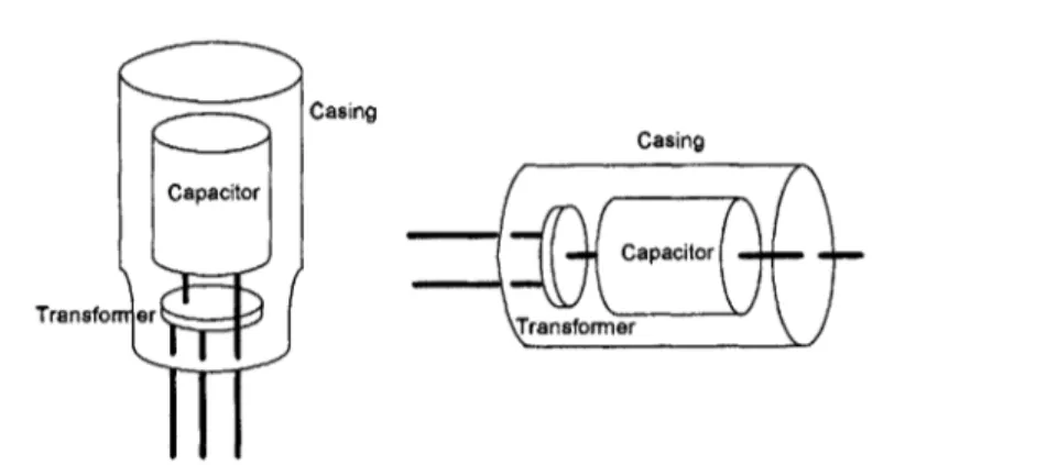
4.1 An integrated filter element with an air core transformer that is wound around and connected to the capacitor and enclosed in the capacitor cas-in g . . . . 76
4.2 Structure of an integrated filter element with a separately constructed trans-former connected to the capacitor and enclosed in a case. . . . . 77
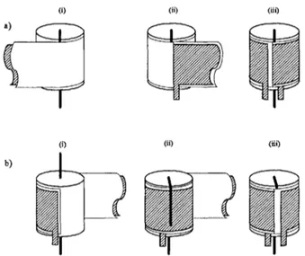
4.3 Winding methods and connections for (a) an end-tapped inductance cancel-lation transformer and (b) a center-tapped inductance cancelcancel-lation transformer. 78 4.4 The winding description of an end-tapped transformer and the associated T model. . ... ... ... .. .. .. .. .. . 78
4.5 The test circuit used for measuring systems with inductance cancellation. . 82 4.6 A prototype integrated filter element based on a United Chemi-Con U767D, 2200 pF, 35 V electrolytic capacitor and center-tapped cancellation winding. 84 4.7 Comparison of a United Chemi-con U767D, 2200 pF electrolytic capacitor to the corresponding prototype integrated filter element. . . . . 84
4.8 A patterned 10 mil thick copper sheet suitable for folding into a transformer. 86 4.9 The transformer formed by adding an insulation layer of clear foil to the planar winding pattern and folding it. . . . . 87
4.10 The prototype integrated element system in which the capacitor terminal is connected to the transformer. The system is now the three terminal de-vice which can be tested after a piece of mylar tape is added to isolate the transformer from the pcb. . . . . 88
4.11 Epoxy is used to coat the transformer to create one solid three terminal device. 89 4.12 The outline of the winding pattern used in the prototype. . . . . 90
4.13 The footprint of the integrated filter element. . . . . 90
4.14 Performance results of the device under test using the device shown above. The higher curve shows a typical capacitor. The lower curve shows the prototype integrated filter element with inductance cancellation. . . . . 91
4.15 Performance results of Fig. 4.14 up to 500 MHz. . . . . 92
5.1 The schematics (a) of an ideal L-section filter and a "T-filter". . . . . 97
List of Figures
5.3 The structure of the "zero-ripple" filter (a). . . . . 98
5.4 A buck converter can use the modified T-filter to replace the buck inductor. 99 5.5 Two examples of variable inductors. . . . . 100 5.6 The relationship between the variable inductance under small-signal ac
con-dition vs. the control current. . . . . 101 5.7 A schematic (a) of a T-filter and a corresponding L-section when parasitic
capacitance is considered. . . . . 103 5.8 A (b) PSpice simulation comparing the attenuation of an (a) L-section filter
and a modified T-filter. . . . . 106
5.9 The three different filters that will be compared. . . . . 106 5.10 A simplified schematic of the experimental dc/dc converter. . . . . 107 5.11 The output ripple (frequency domain measurement) of the dc/dc converter
using (a) an L-section filter, (b) a "zero-ripple" filter, and (c) a T-filter with actively tuned inductance cancellation. . . . . 108 5.12 The output ripple (time domain measurement) of the dc/dc converter using
(a) an L-section filter, (b) a "zero-ripple" filter, and (c) a T-filter with actively tuned inductance cancellation. . . . . 109 5.13 A comparison between an L-section filter, a modified T-filter and a LFe filter 110
6.1 A typical current sensing scheme. A differential amplifier measures the
volt-age drop of the sense resistor. ... ... 114
6.2 A current sense resistor and amplifier that used two capacitors to add a pole
that will offset the zero caused by the inductance of the sense resistor. . . . 115 6.3 A schematic (a) and picture (b) of the test setup of a resistor with inductance
cancellation. . . . . 116
6.4 The sensed output voltage due to a constant magnitude input frequency sweep of a current sense resistor and an operational amplifier with and with-out a pole at low frequencies. . . . . 117 6.5 The sensed output voltage due to a constant magnitude input frequency
sweep of a current sense resistor with and without inductance cancellation and an operational amplifier. . . . . 118 6.6 A rectifier circuit in which the equivalent series inductance of the diode can
be adjusted with inductance cancellation. . . . . 119 6.7 A second rectifier circuit in which the equivalent series inductance of the
diode can be adjusted with inductance cancellation. . . . . 120
-List of Figures
6.8 An inverter circuit in which the equivalent series inductance of the diode can
be adjusted with inductance cancellation. . . . . 120
7.1 A simple inductor model including parasitic effects. . . . . 123
7.2 A test circuit for evaluating the filtering performance of magnetic components. 125
7.3 An additional winding and a capacitor are added to the inductor to form the
circuit for parasitic capacitance cancellation. . . . . 126
7.4 Ratio of input to output voltage for the P3219-A Coilcraft choke. . . . . 128
7.5 Ratio of output to input voltage for the P3219-A Coilcraft choke in which
the turns ratio of the transformer is changed from 0.5 to 0.06. . . . . 130
7.6 The effects of changing the coupling coefficient on the system in Fig. 7.2. . 131
7.7 The effects of changing the term CcompLcomp,, the total series capacitance
and inductance in the compensation path, on the improvement of attenuation
at 20 M H z. . . . . 132
7.8 An equivalent circuit model showing how capacitance cancellation can be
implemented using a parallel RF transformer to inject cancellation currents. 132
7.9 Performance of a filter inductor with and without capacitance cancellation. 134
7.10 The schematic for the common mode choke with capacitance cancellation
and setup for a common mode test. . . . . 135
7.11 A photograph of the FN2010-6-06 filter with external capacitance cancellation. 135 7.12 A plot comparing the performance of the common mode response of an EMI
filter, Schaffner FN2010-6-06, and one modified with capacitance cancellation
as shown schematically in Fig. 7.10. . . . . 136
7.13 A PSpice simulation examining the differential mode noise that results from
a common mode disturbance for the system shown in Fig. 7.10. . . . . 137
A.1 The typical model of a transformer. . . . . 144
A.2 A physically-based circuit model of the end-tapped coupled magnetic windings. 144 A.3 The test setup to determine LBC. . . . . . . . . . . . . 145
A.4 The Delta and T models for a three terminal device. . . . . 146
A.5 A physically-based circuit model of the center-tapped coupled magnetic
wind-in gs. . . . . 146
List of Figures
-3.1 A comparison of an end-tapped and a center-tapped transformer. . . . .
3.2 Comparison of values of inductance calculated and measured using a variety
of sources... ...
3.3 Experimental verification of FastHenry simulations of groundplane. . . . . .
4.1 Inductances of Metal foil wrapped around United Chemi-Con U767D, 2200
,4F, 35 V capacitor for various number of turns. . . . . Constants . . . .
Stamping machine cost . . . . Spraying machine cost . . . . Folding machine cost . . . . Potting material injector machine cost . . Welding machine head cost . . . . Copper cost for an integrated filter with a Adhesive cost . . . . Potting material cost . . . . Adhesive cost . . . . . . . . 154 . . . . 154 . . . . 154 . . . . 155 . . . . 155 . . . . 155 dc current rating of 2.58 A. . . . 156 . . . . 156 . . . . 157 . . . . 157
List of Tables
54 58 67 81 C.1 C.2 C.3 C.4 C.5 C.6 C.7 C.8 C.9 C.10List of Tables
-Chapter 1
Introduction
1.1
Background
No real electrical element is ideal. Wherever a current loop exists, an inductance can be found. Wherever two conductors are near each other, a capacitance can be found. Real electrical elements can be well modeled by their ideal element for only the range of frequencies in which the parasitic components are negligible. Outside of this range the impedance of real electrical elements will be dominated by their parasitic components. To reflect this, the real electrical element can be modeled with a collection of ideal parasitic inductors, capacitors, and resistors. These models classify the parasitics that influence the high- and low-frequency operation of real elements. This thesis addresses filter and filter component design that will compensate for the parasitic effects present in electrical elements. We start by examining the high frequency models of two of these elements, the capacitor and the inductor. Also we will be examining how the presence of parasitic effects in these passive elements affects the design of filters for power applications.
1.1.1 Capacitors
High frequency models for capacitors have been well established [1]. One such model, shown in Fig. 1.1a, shows an ideal capacitor in series with a resistor (RESR) and an inductor
(LESL). This parasitic resistance is a combination of the lead resistance and the dielectric
losses in the capacitor. (The dielectric resistance is in parallel with the capacitor but it is usually lumped into a frequency dependant series resistance.) The parasitic inductance is caused by the capacitor current and its associated stored magnetic energy storage associated with the current loop. At low frequencies the impedance of the capacitor is dominated by
Introduction
a) b) C)
LESL
R ESRj
C
S.R.E Log Freq.
Figure 1.1: (a) The high frequency model of a typical capacitor, (b) the magnitude of the impedance as a function of frequency and (c) the plot of the magnitude of the impedance of an X-type (safety) capacitor (Beyschlag Centrallab 2222 338 24 224, 0.22 /IF, 275 Vac).
the ideal capacitance in the model. (At very low frequencies the capacitor impedance is dominated by a contact surface resistance or insulation resistance that is in parallel with the capacitance; this parasitic is not considered here.) At higher frequencies though, the inductive parasitic elements will dominate the performance of the capacitor. Figure 1.1b schematically shows a typical capacitor's impedance as a function of frequency. Figure 1.1c shows an impedance plot of an X-type (safety) capacitor (Beyschlag Centrallab 2222 338 24 224, 0.22 jpF, 275 Vac). The frequency in which a capacitor changes from acting capacitive to inductive is called the self-resonant frequency. For example, a typical aluminum electrolytic capacitor may appear inductive (impedance rising with frequency) at frequencies above 50-100 kHz, limiting its ability to shunt ripple at high frequencies. Similarly, large-valued film
capacitors typically become inductive in the range of 100 kHz - 1 MHz. While not perfect,
this capacitor model forms a good basis for developing improved components and filters.
1.1.2 Inductors
Inductors can also be modeled with two main parasitic components as shown in Fig. 1.2a. There exists a parasitic resistance in series with an ideal inductor and a parasitic capacitance in parallel with the inductor. This resistor models the power losses in an inductor including the winding resistance of the wire and magnetic losses in the core. (The magnetic losses represent a resistance in parallel with the inductor, this resistance is usually converted into a
1.1 Background
a) a) b) d4C c)
CPAR
RpAR~ L
S.R.F Log FReq.
Figure 1.2: (a) The high frequency model of a typical inductor, (b) the magnitude of the impedance as a function of frequency and (c) the plot of the magnitude of the impedance for an inductor (Scohtt 67127100 680/muH.)
frequency dependent series resistance. In general, the effective resistance that is observed is frequency dependent, but we neglect this effect at present.) The parasitic capacitance exists because of the proximity of the windings to each other. Any two individual turns will have different voltages (due to induction and voltage drops caused by the winding resistance), and the displacement currents that consequently flows across turns can be modeled with a parasitic capacitance. This parasitic capacitance depends on the size and arrangement of the windings. The parasitic resistance affects the impedance of the inductor at low frequencies. At high frequencies the parasitic capacitance will dominate the impedance of the inductor. Figure 1.2b schematically shows the impedance of the inductor across a wide range of frequencies. Figure 1.2c shows the impedance of the Scohtt 67127100 680pH inductor. The self-resonant frequency of inductors are often significantly greater than the self-resonant frequency of capacitors for many filter designs of practical interest. The self-resonant frequency of an inductor is usually in the range of 5-10 MHz and higher though in common-mode inductor designs it is often lower. Again, the model of Fig. 1.2b is a simplification of the actual behavior of practical devices, but it is a good basis for developing improved components and filters.
1.1.3 Filters
Electrical filters are designed to prevent unwanted frequency components from propagating from the filter input port to the filter output port, while passing desirable components. In
Introduction
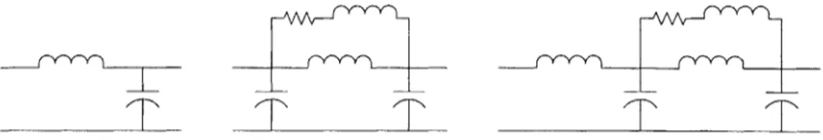
Figure 1.3: Some common low-pass filter structures for power applications.
power applications, filters are important for attenuating electrical ripple, eliminating elec-tromagnetic interference (EMI) and susceptibility, improving power quality, and minimizing electromagnetic signature. One byproduct of switching power converters is the generation of unwanted high frequency signals at the input and output of the converter. EMI filters for DC outputs typically employ capacitors as shunt elements, and may include inductors as series elements, as illustrated in Fig. 1.3. The attenuation of a filter stage is determined
by the amount of impedance mismatch between the series and shunt paths. For a low-pass
filter, minimizing shunt-path impedance and maximizing series-path impedance at high fre-quencies is an important design goal. Design methods for such filters are described in [2] and [3], for example. The parasitic components of the capacitor and inductor will affect the performance of a filter. An ideal inductor and capacitor would be perfect for the series and shunt paths respectively. However, an ideal low pass filter cannot be made with non-ideal components. The parasitic elements in the filter will, at some frequencies, control the attenuation of the filter.
Let us examine the operation of a two element filter with a resistive load that is shown in Fig. 1.4a with all of its high frequency parasitic elements. A simulation of the filter is shown in Fig. 1.4b. There are three different frequency ranges to examine. At frequencies lower than the self-resonant frequency of the capacitor, the filter behaves like an ideal low pass filter. The mid-frequency range is above the self-resonance of the capacitor and below the self-resonance of the inductor. In this range the filter operates like a voltage divider made up of inductors. The attenuation is constant and approximately
LESL 11 LLoad
LESL 1 LLoad + L
Where LLoad is the parasitic inductance of the load resistor. Note that in order to increase performance in the mid-frequency range increasing the capacitance is not helpful. Typically,
-1.1 Background a) b) CPAR~ 5pF RpAR L 40pfH .28. jLESL 15.2nH Load l0nH RESR 90M.Q C RLoa 220pF 50a
Figure 1.4: (a) A low pass filter made up of high frequency component models and (b) the voltage gain of the filter based on frequency. At frequencies below 10kHz the low pass filter looks ideal, but after 1 MHz the gain is not decreasing by 40 dB per decade and is relatively constant and after 10 MHz the gain increases.
larger capacitors have more equivalent series inductance which, for this frequency range, lowers the amount of attenuation. The traditional approach to overcoming filter capacitor limitations is to parallel capacitors of different types (to cover different frequency ranges) and/or to increase the order of the filter used (i.e., using more filter elements in a larger filter design). Both of these approaches can add considerable size and cost to the filter.
At frequencies above the self-resonance of the inductor, the capacitor is dominated by its parasitic series inductance and the inductor is dominated by its parasitic parallel capacitance, thus the capacitor looks inductive and the inductor looks capacitive. In this range the filter operates like a high pass filter. With an attenuation of
Vout (LESL 1 LLoad)Cpars2
Vin (LESL 11 LLoad )CparS2 + 1
At high enough frequencies, additional parasitics that have not been modeled will affect the performance of the filter. These higher order parasitic elements are usually undefined since their behavior is difficult to predict and the presence of the modeled parasitic elements usually dominate the performance of the component over the frequency range of interest.
Introduction
1.2
Thesis Objectives and Motivation
The objective of this thesis is to improve the high frequency performance of components and filters by better compensating the parasitic effects of practical components. The main ap-plication for this improvement is in design of low pass filters for power electronics, although some other applications will be presented.
In switching power supplies the input and output filters must attenuate frequencies related to the fundamental switching frequency of the converter. The filters represent a major contribution to the weight, volume and price of the power supply. Therefore, aspects of the design of the switching power converter, especially those related to the switching fre-quency, are limited by the high frequency performance of the filters. The usual methods of improving the high frequency performance of the filter includes using larger, better compo-nents. Filter performance can improve by using higher quality inductors and capacitors or by adding high frequency capacitors in parallel with the filter capacitor. Also, an additional filter stage can be added. All of these methods add significant cost to the design of the
power supply.
If the effect of high-frequency parasitic elements in the components can be reduced (at a low cost) the performance of the filter can be enhanced. This allows the development of filters with much better high frequency attenuation, or the reduction of filter size and cost at a constant performance level. In filtering and other applications, the ability to reduce the effect of parasitic elements will be a technique that will enable many high-frequency designs.
Specifically, this thesis will present two techniques that can be used to reduce the effects of parasitic inductance and capacitance. One technique, called inductance cancellation, is used to reduce the amount of parasitic inductance in a path of interest. The other technique, capacitance cancellation, will reduce the effect of a parasitic capacitance in an inductor. The techniques introduced here cannot be used to improve performance of passive components in all applications. These techniques, though, do provide major improvements in most filtering applications, an application in which parasitic components play a central role in the design.
-1.3 Thesis Overview
1.3
Thesis Overview
This thesis will introduce inductance cancellation and capacitance cancellation techniques. These techniques and their effects will be demonstrated in various circuits. Design guidelines for practical application of these principles are also developed and validated.
Chapter 2 fully explains the principles of inductance cancellation and experimentally demonstrates the use of the approach. Chapter 3 examines the design of filters with induc-tance cancellation in which the circuitry realizing cancellation is implemented using traces on a printed circuit board (pcb). Generally, the area needed on the pcb is comparable to the footprint of the component and can be placed under the component. Chapter 4 examines the design of components in which inductance cancellation windings are integrated with a capacitor to form an integrated filter element. Chapter 5 examines a design approach in which inductance cancellation can be adjusted with active control, allowing its use in appli-cations where the parasitic inductance is not well known or controlled. Chapter 6 looks at some uses of inductance cancellations in applications other than filtering. Chapter 7 intro-duces and capacitance cancellation technique and its application improving the performance of inductors and common-mode chokes. Finally, Chapter 8 concludes the thesis.
Introduction
-26-Chapter 2
Filters and Components with Inductance
Cancellation
2.1
Introduction
Inductance cancellation is a passive circuit technique that effectively shifts inductance from a circuit branch where it is undesirable to other branches where it is acceptable. In circuit terms, a consequence of the technique to be proposed will essentially provides a negative inductance in one circuit branch, and larger positive inductances in other circuit branches. The negative inductance can be placed in series with an unwanted parasitic inductance, thereby improving the high-frequency performance of the circuit. Therefore, the total in-ductance in the system will increase, not decrease, when inin-ductances in one branch is shifted to two other branches.
The technique of inductance cancellation is well suited to improve the performance of capacitors, especially for their use in electrical filters. Capacitors are critical elements in such filters, and filter performance is strongly influenced by the capacitor's parasitics. This chapter introduces the application of this new design technique to overcome the capacitor parasitic inductance that limits filter performance at high frequencies. Coupled magnetic windings are employed to effectively cancel the parasitic inductance of capacitors, while adding inductance in filter branches where it is desired. The underlying basis of the new technique is treated in detail, and its application to the design of both discrete filters and integrated L-section filter components is described. Numerous experimental results demonstrating the high performance of the approach in both discrete filters and integrated filter elements are provided.
Filters and Components with Inductance Cancellation A.
~11
ii 22 CFigure 2.1: An end-tapped connection of coupled magnetic windings.
2.2
Inductance Cancellation
2.2.1 End-tapped Transformers
Magnetically-coupled windings can be used to cancel the effects of capacitor parasitics. Fig. 2.1 illustrates one possible connection of coupled magnetic windings, which we hereafter refer to as an "end-tapped" connection. In this case, each winding links flux with itself and
mutually with the other winding. An electromagnetic analysis of this system leads to an
inductance matrix description:
[A
1
1F
N2 N2 1 r1
-
+
2 L1 1 LM 1ii~ANj
N
N2i
2J- LL
2
J
2
1(2.1)
1\2 1 W N + jM 2 Lm L22 i2
where the flux linkages A, and A2 are the time integrals of the individual coil voltages, and
i1 and i2 are the individual coil currents. The self-inductances L11 and L2 2 and mutual
inductance LM are functions of the numbers of coil turns and the reluctances R1
1, R22,
and RM of the self and mutual magnetic flux paths. In cases where no magnetic material is present, the behavior of the coupled windings is determined principally by the geometry of the windings. Conservation of energy considerations require that the mutual coupling between the windings be less than or equal to the geometric mean of the self-inductances.
-2.2 Inductance Cancellation
A LM L22~-LM B
L11 -LM
Figure 2.2: An equivalent circuit model for end-tapped coupling magnetic windings.
That is,
LM V'L 1 1L2 2 (2.2)
Thus, the inductance matrix of (2.1) is necessarily positive semidefinite. Note that while
the constraint (2.2) limits Lm to be less than or equal to the geometric mean of L11 and L22,
it may still be larger than one of the two inductances. For example, with proper winding of the coils one may have
L11 < Lm < L1 1L2 2 < L2 2 (2.3)
Figure 2.2 shows one possible equivalent circuit model for the coupled inductor windings based on the inductance matrix of (2.1). This model is referred to as the "T" model of the coupled windings and is derived in Appendix A. With the ordering of self and mutual
inductances of (2.3), the inductance of one leg of the T model - the vertical leg in Fig. 2.2
- is clearly negative! It is this "negative inductance" that will be used to overcome the
high-frequency limitations of filter capacitors.
The negative inductance effect arises from electromagnetic induction between the cou-pled windings. This is readily seen in the physically-based circuit model of the coucou-pled windings shown in Fig. 2.3. (With appropriate parameter values, the circuit models of Fig. 2.2 and Fig. 2.3 have identical terminal characteristics, and each captures the behav-ior of the system (2.1).) Appendix A examines several popular transformer models and demonstrates the conversion of the physically based model of Fig. 2.3 to the form shown in Fig. 2.2, which is the most useful representation of the transformer in this application. We stress that the negative inductance in the T model does not violate any physical laws. Only one leg of the T model has a negative inductance. The total inductance seen across
Filters and Components with Inductance Cancellation
N2 : Nj
L11 =f (LI1, L12, LM,N N
L12 =f (L1l, Ll2, LM,N N
Lp = f(Ll1, L12, LM, N NI
Figure 2.3: A physically based circuit model of the coupled magnetic windings. The formulae converting from these parameters to L11, L22, and Lm are in Appendix A.
any winding is -as expected -the positive-valued self inductance of the winding.
Fig. 2.4 shows the application of the coupled magnetic windings to a capacitor whose
equivalent series inductance (ESL) is to be cancelled. The coupled windings are modeled with the T network of Fig. 2.2, while the capacitor is shown as an ideal capacitor C in series with parasitic resistance RESR and parasitic inductance LESL. (We also lump any interconnect parasitics into these elements.) When L1 1 - LM is chosen to be negative and close in magnitude to LESL, a net shunt path inductance AL = L1 - LM - LESL 0
results. The combined network is very advantageous as a filter. A near-zero shunt path impedance (limited only by ESR) is maintained out to much higher frequencies than is possible with the capacitor alone. Furthermore, as L2 2 is much greater than LM, the series-path inductance L2 2 - LM serves to either increase the order of the filter network or is in series with another filter inductor, both options will improving filter performance.
The voltage stress across the capacitor will go up slightly. Assume that, at a particular frequency, 99 % of the ac current will travel through the capacitor rather than the load. Also assume that using inductance cancellation will improve filtering by a factor of 10. Therefore with inductance cancellation 99.9 % of the ac current will travel through the capacitor. The increase in ac current will correspond to a small increase in voltage across the capacitor.
An improvement in filter performance can be seen by examining the effect of inductance
-2.2 Inductance Cancellation LM L22 -LM L11 -LM LESL RESR C
Figure 2.4: Application of coupled magnetic windings to cancel the series inductance of a capacitor. Capacitor ESR and ESL are shown explicitly, along with the equivalent T model of the magnetic windings.
cancellation on (1.1) which is repeated below.
LESL 1 LLoad LESL 11 LLoad + L
This equation gives the approximate attenuation of a second order low pass filter in a fre-quency range in which the parasitic inductance dominates the impedance of the capacitor. Two things should be considered when examining this equation when inductance cancella-tion is applied. Normally to improve the attenuacancella-tion the filter needs either a larger inductor or a better quality capacitor (with less parasitic inductance). With inductance cancellation the value of LESL will be reduced by a factor of 10 or more and the values of LLoad and L will be increased by an amount larger than LESL but on the same order of magnitude. The term LESL 1 LLoad will thus be greatly reduced by inductance cancellation and improve the filter performance. Also, because of inductance cancellation the frequency at which parasitic inductance starts to dominate the performance of the capacitor will be higher, and therefore the filter will look like a second order system for a wider range of frequencies. In the previous chapter it was stated that all inductors (and transformers) have parasitic capacitors that will impair their performance at high frequency. The inductance cancellation transformer should be designed so as to have a negligible capacitance. Typical inductors and transformers with magnetic cores have a limited winding area and a large desired
Filters and Components with Inductance Cancellation
A B
011 22
C
Figure 2.5: A center-tapped coupled magnetic winding configuration.
inductance, in order to minimize the volume of the structure, the windings are packed in close proximity to each other. Transformers for inductance cancellation do not need a lot of turns to achieve the desired inductances and are not limited to a prescribed winding area. Also, the self-resonant frequency of the transformer will be extremely high (typically far higher than the conduction EMI frequency range) since the inductances are so small.
2.2.2 Center-tapped Transformers
It should be appreciated that the other connection method of the magnetic winding struc-ture can also be used to realize inductance cancellation. Another three-terminal coupled magnetic structure that can be used is shown in Fig. 2.5. This implementation is advanta-geous in that it can be formed from a single winding tapped at an appropriate point. An electromagnetic analysis of the system of Fig. 2.5 results in an inductance matrix:
A,
-NN 2 1 i I [ L1 1 -LM ii_1_ R N2 N2
=
(2.5)
2 2 2 2 _
i2
_-LM L2 2i2
where the self inductances L11 and L22 and mutual inductance LM are again functions of
the numbers of coil turns N1, N2 and the reluctances of the respective magnetic flux paths.
The magnitude of the mutual inductance is again limited by the constraint (2.2), though without the ordering imposed in (2.3).
The terminal characteristics of the system of Fig. 2.5 can be modeled with the "T model" of Fig. 2.6 following the steps outlined in Appendix A.3. Again, one branch of
-2.3 Implementation
LM+L1I L22+LM
A B
-LM
Figure 2.6: An Equivalent circuit model for the center-tapped coupled magnetic windings.
the T model has a negative inductance (in this case equal in magnitude to the mutual inductance LM). When LM is chosen to be close in magnitude to the equivalent series
inductance LESL of an electrical circuit path (e.g., through a capacitor) connected to the
bottom terminal, a reduced net effective inductance AL = -Lm -+ LESL ~ 0 results in the
capacitor's shunt path.
As described above, coupled magnetic windings are used to cancel inductance in the capacitor branch (e.g., due to capacitor and interconnect parasitics) and provide filter in-ductances in the other branches. In a low-pass filter, this corresponds to a cancellation of the filter shunt branch inductance, and an addition of series branch inductance. (The final branch path necessarily has an inductance greater than or equal to the magnitude of the "negative" inductance that is introduced in the capacitor path.) We point out that the use of coupled magnetics in filters is not in itself new. In fact, use of coupled magnetic windings in filters dates at least as far back as the 1920's [4], and has continued up to the present time in many forms [5-10] (see [5] for a good review of such usage). The approach described here differs from these existing methods in that the coupling of the windings is used to cancel the effects of parasitic inductance in the capacitor and interconnects, permitting dramatic improvements in filtering performance to be achieved.
2.3
Implementation
In this section we consider application of this inductance cancellation technique to the design of both discrete filters and integrated filter components. One important design consideration is that of variability: if tuning of individual units is to be avoided, the inductances of both
Filters and Components with Inductance Cancellation a) it- 9- 8- 7-6 5 4 3 2
U767D ESL distribution U767D ESR distribution
b) 9-8 7 6 5 4 3 2 1-0 10 20 30 0 15 so
ESL (nH) ESR (mu)
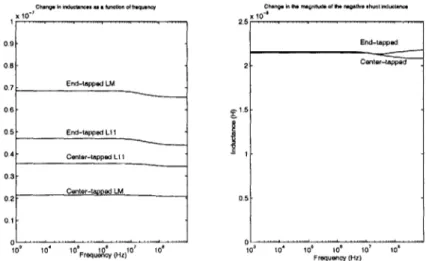
Figure 2.7: (a) ESL and (b) ESR histograms for 30 United Chemi-Con U767D 2200 pLF 35 V capacitors. ESL range: 17.29 to 18.13 nH, a = 44.6 pH. ESR range: 14.2 mQ to 60.9 mQ (outlier not shown).
the capacitor and the magnetic windings must be consistent from component to component1 . Fortunately, unlike capacitance or ESR values, capacitor ESL is typically consistent to within a few percent. For example, the histograms of Figs. 2.7(a) and 2.7(b) show the distribution of ESL and ESR for a type of electrolytic capacitor that is widely used in filters. The ESR varies over a wide range from 14.2 mQ to 60.9 mQ (outlier not shown). The ESL, by contrast, varies only from 17.29 nH to 18.13 nH (with a standard deviation of 44.6 pH), representing a maximum variation in ESL of only ±2.4% across units. This makes sense: the absence of magnetic materials means that the inductance of the structure depends primarily on geometry, while capacitance and resistance depend on material and interface properties. One may conclude that inasmuch as appropriate coupled-magnetic structures can be created, the parasitic inductance can be repeatably cancelled to within a few percent of its original value.
The capacitor inductance to be cancelled in a practical design is typically quite small (on the order of tens of nanohenries). Coupled magnetic windings appropriate to the can-cellation technique must thus be able to accurately generate a negative effective shunt inductance in this range under all operating conditions. One approach for achieving this is to use coupled windings without magnetic materials. Such "air-core" magnetics are appro-priate given the small inductances needed and the desire for repeatability and insensitivity 'Systems incorporating active self tuning [11-13] (e.g., via controllable magnetics [14-17]) are also pos-sible. We defer consideration of this approach to chapter 5.
- 34
-4
r1,
0
2.3 Implementation
to operating conditions.
Two approaches for employing the proposed inductance cancellation technique are con-sidered in this thesis. We first address the use of inductance cancellation methods in the design of filter circuits built with discrete components (e.g., capacitors and inductors) using conventional manufacturing techniques. We then explore the integration of cancellation
windings with a capacitor to form an integrated filter element - a three terminal device
providing both a shunt capacitance (with extremely low shunt inductance) and a series inductance.
2.3.1 Discrete Filters
An immediate application of the proposed technology is in the design of discrete filters
-that is, filters built with available or easily manufactured components using conventional fabrication techniques. In this approach, a coupled winding circuit is connected to a discrete capacitor to provide a very low-inductance path through the capacitor along with a second high-inductance path. The coupled winding circuit should have repeatable inductance pa-rameters (that are properly matched to the capacitor), and should have minimal size and cost impact on the filter.
One simple implementation method is to print the coupled windings as part of the filter printed circuit board (PCB). Printing the magnetic windings on the PCB results in extremely repeatable magnetic structures and interconnects. Furthermore, it represents essentially no extra cost or volume in the design if the PCB space underneath the filter capacitor can be used for the windings.
We have found air-core PCB windings to be highly effective for the proposed induc-tance cancellation technique. As will be demonstrated in Section 2.4, practical printed PCB windings can be implemented using either end-tapped (Fig. 2.1) or center-tapped (Fig. 2.5) winding configurations, and can be placed either partially or entirely underneath the capac-itor on the PCB. A two-layer circuit board is typically sufficient to implement the windings with the required interconnects accessed at the outside of the spiral windings. The cou-pled winding circuits demonstrated here were designed using a widely-available inductance calculation tool [18] and refined experimentally.
Filters and Components with Inductance Cancellation
D
C
Figure 2.8: Integrated filter element D is constructed by adding magnetically-coupled windings A and B over, or as part of, the basic capacitor structure. The integrated filter element is then a three-terminal device, with the connection of the two magnetic windings brought out as terminal C.
2.3.2 Integrated Filter Elements
In addition to their application in discrete filters, inductance cancellation techniques have application to new filter components. Here we introduce the integration of coupled magnetic windings (providing inductance-cancellation) with a capacitor to form an integrated filter element - a single three-terminal device providing both a shunt capacitance (with extremely low inductance) and a series inductance. To do this, one can wind inductance-cancellation magnetics on, within, or as part of the capacitor itself. This approach, illustrated in Fig. 2.8, minimizes the volume of the whole structure, as the same volume is used for the capacitive and magnetic energy storage. For example, starting with a wound (tubular) capacitor, one could wind the coupled magnetics directly on top of the capacitor winding. The magnetic windings can also be implemented through extension or patterning of the capacitor foil or metallization itself. An integrated filter element utilizing inductance cancellation may be expected to have far better filtering performance than a capacitor of similar size. We note that components incorporating both capacitive and inductive coupling have a long history in power applications [19-25] and continue to be an important topic of research (e.g., [26-29]). However, the aims and resulting characteristics of such prior art integrated elements are quite different than those described here. The approach described here is different in that magnetically-coupled windings are used to nullify the effects of the parasitic inductance in the capacitive path. This permits, with relatively modest changes in manufacturing methods, dramatic improvements in filtering performance to be achieved as compared to conventional components.
-2.3 Implementation
As with discrete filters, both end-tapped and center-tapped coupled-winding configu-rations are possible. (Note that in some integrated implementations, flux associated with current flow in the capacitive element may link the cancellation windings. This changes
the details of the magnetic analysis -and may be used to advantage - but the underlying
principles remain the same.) Consider an integrated component having a wound structure, as suggested by Fig. 2.8. In an end-tapped configuration, the magnetic windings comprise two conductors co-wound and electrically connected at one end (one terminal of the three terminal device.) The other end of one conductor is a second terminal of the device. The other end of the second conductor is connected to one plate of the capacitor. (The magnetic winding may be formed as a direct continuation of the capacitor winding in this case.) The other plate of the capacitor is connected to the third terminal. A basic magnetic analy-sis of this structure will assume that there are no fringing fields and flux due to parasitic inductances are well shielded by the capacitor, therefore the capacitor can be modeled as a cylindrical metal enclosure. A more advanced version will model several of the outer layer of the capacitor but the significance of the fringing fields will be low. Regardless of which model is used, a design iteration can be used to identify a design that has consistent performance.
In a center-tapped magnetic winding configuration, the coupled magnetic windings may be formed as a single conductor wound concentrically with the capacitor windings. The magnetic winding is tapped (connected to one plate of the capacitor) at a specified point in the winding. The other plate of the capacitor and the two ends of the magnetic winding form the three terminals of the device. Fig. 2.9 illustrates one possible method for forming the cancellation winding over the capacitor structure and interconnecting it to one capacitor plate.
Another manner of incorporating inductance cancellation directly into the capacitor is to build small transformers and to connect them to the leads inside the capacitor. A loop of metal can be made into a transformer, this transformer can be encapsulated in a non-conducting material. Three connection points can be made from the transformer to the rest of the capacitor. The capacitor packaging can enclose both the capacitor and the transformer.
Filters and Components with Inductance Cancellation
Figure 2.9: One construction method for an integrated filter element with a center-tapped winding.
2.4
Experimental Results
In this section we demonstrate the viability and high performance of the proposed in-ductance cancellation technology. We validate the approach for both discrete filters and integrated filter elements across a variety of capacitor sizes and types, and with both end-tapped and center-end-tapped winding configurations. The choice between end-end-tapped and center-tapped transformers were made arbitrarily in this section so as to show examples with each configuration. In the next chapters comparison between the two transformer styles will be made. We also demonstrate the large performance advantage of a prototype integrated filter element in a power converter application.
2.4.1 Evaluation Method
To evaluate the effectiveness of the inductance cancellation method, the test setup of Fig. 2.10 is used. The device under test (DUT) is either a capacitor, a capacitor plus PCB cancellation windings, or an integrated filter element. The DUT is driven from the 50
Q output of the network analyzer. As the driving point impedance of the DUT is always
far less than the output impedance of the network analyzer, the drive essentially appears as a current source. The voltage response is measured at the 50 Q load of the network an-alyzer. The input impedance of the network analyzer is much greater than the impedance associated with the series output inductance of the DUT for the frequencies under
-2.4 Experimental Results
Network Analyzer DUT Network Analyzer
Source Load
Figure 2.10: An Experimental setup for evaluating filters and components. The Network analyzer is an Agilent 4395A.
ation. Accordingly, this test effectively measures the shunt impedance of the DUT relative to the 50 Q load impedance of the network analyzer. Thus, this test focuses on filtering improvements associated with the shunt-path inductance cancellation, while suppressing improvements available through the introduction of series path inductance. In the practical application of a filter, one could take advantage of the series inductance provided by the cancellation windings to further improve attenuation performance.
It should be noted that all measurements of capacitor performance at frequencies up to 30 MHz need to be carefully performed. A circuit layout that includes large parasitic inductive loops can induce a signal on par with (or greater than) the signal to be measured. To ensure proper measurement of filter performance the input and output connections to the
network analyzer can be made with BNC to PCB connectors. Testing performed without these connectors used a pair of twisted wires to make the connection to the capacitor. In that setup the signals received by the twisted pair were up to an order of magnitude greater than the output ripple to be measured. The resulting test setup had performance that was dependant on the positions of all the connections to the capacitor circuit. Further tests of the noise floor (a test in which the connection to the capacitor from the network analyzer was made with twisted pair, but the output is left disconnected) showed that the receiver would pick up significant amounts of radiated noise. All measurements made in a test stand with low inductance connections to the board did not have this problem.