HAL Id: hal-01630685
https://hal.archives-ouvertes.fr/hal-01630685
Submitted on 8 Nov 2017HAL is a multi-disciplinary open access archive for the deposit and dissemination of sci-entific research documents, whether they are pub-lished or not. The documents may come from teaching and research institutions in France or abroad, or from public or private research centers.
L’archive ouverte pluridisciplinaire HAL, est destinée au dépôt et à la diffusion de documents scientifiques de niveau recherche, publiés ou non, émanant des établissements d’enseignement et de recherche français ou étrangers, des laboratoires publics ou privés.
Optimal compensation capacitors maximizing coreless
inductive power transfer
Yohan Wanderoild, Adrien Morel, Romain Grézaud, Gaël Pillonnet,
Dominique Bergogne, Hubert Razik
To cite this version:
Yohan Wanderoild, Adrien Morel, Romain Grézaud, Gaël Pillonnet, Dominique Bergogne, et al.. Optimal compensation capacitors maximizing coreless inductive power transfer. PCIM Europe 2017, May 2017, Nuremberg, Germany. �hal-01630685�
Optimal compensation capacitors maximizing coreless inductive
power transfer.
Yohan Wanderoild1, Adrien Morel1, Romain Grezaud1, Gael Pillonnet1, Dominique Bergogne1, Hubert
Razik2
1Univ, Grenoble Alpes, F-38000 Grenoble, France
CEA, LETI, Minatec Campus F-38054 Grenoble, France
2 Universite Claude Bernard Lyon 1, AMPERE UMR CNRS 5005, Villeurbanne, France
Contact: [email protected]
Abstract
The use of coreless transformers is still limited because of the power they can transmit and the reactive power they absorb. This paper introduces a comprehensive theoretical approach of the transferable power and the related compensation topologies allowing to optimize the system used. Analytical equations are given in order to estimate the maximum power transmission of a coreless transformer. Based on the theoretical results the optimal topology can then be selected accordingly to the power source, the transformer and the sensibility over the deviations of the elements. This methodology has been validated experimentally and allowed to transmit 2W through a 2.25cm² coreless transformer under 1 MHz. Moreover this results can be broaden to any inductive power transfer system.
Introduction
Coreless transformers also known as coupled coils, allow to transmit power without any physical link, making them the perfect candidates for inductive power transfer (IPT). Indeed, this technology is currently being standardized for electrical vehicle chargers or biomedical implants. Furthermore, the transmission of energy through a magnetic field without a magnetic core allow the system to work at high temperature, high frequency while simplifying the fabrication process. As it also ensure a galvanic isolation, it appears to be an excellent solution for high temperature, high frequency isolated power converters [1], [2].
1. Fundamentals of inductive power
transfer
Firstly, we are going to introduce the fundamental differences between a transformer with or without a magnetic core.
In magnetic core transformers, as explained by Witulski [3], the use of a ferromagnetic core allows to drastically reduce the magnetic energy stored, since the magnetic permeability of the air is drastically lower than the magnetic material one. As a matter of fact, the magnetizing inductor 𝐿𝑚 in Fig. 1 is several decades lower for coupled coils than in a transformer with a magnetic core. Moreover, without the use of a magnetic core, the magnetic field is no longer channeled between the two coils. It significantly decreases the coupling between the two coils and thus the magnetizing
Fig.1 Conventional model of coreless transformers (T; ideal transformer).
inductor, at the cost of an increase of the leakage inductors identified as 𝐿𝑒1 and 𝐿𝑒2 in Fig. 1. Consequently, without proper compensation, the low magnetizing inductor 𝐿𝑚 sinks a lot of current and adversely affects the power transfer from the primary to the secondary side. This inductor stores a significant amount of reactive power which needs to be compensated through harmonics oscillators. This compensation is made thanks to capacitors adequately tuned to the system.
In order to correctly adjust the compensation, the parasitic couplings need to be taken into account. If the working frequency is too close to the self-resonating frequency of the transformer, the interwinding coupling due to the electrostatic coupling between tracks can be substantial enough to affect the compensation. These capacitors which depend on the design of the transformer can be approximated by 𝐶p1, 𝐶p2 and 𝐶12. For simplicity purposes the analytic solutions given are not taking into account these capacitances but the comprehensives solutions can be calculated using the same methodology. A coreless transformer not only needs a significant amount of reactive energy, it also consumes active energy. The losses due to the copper, the current crowding and the skin effect must also be considered. These losses can be modeled by the frequency dependent resistances 𝑅1and 𝑅2. The reactive power sunk by the transformer through the magnetizing inductor 𝐿𝑚 is conventionally compensated with two impedance converters (Fig. 2.).
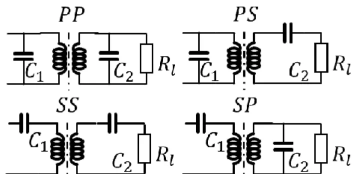
The impedance converters are set to maximize the available output power, they can be made with a serial or a parallel capacitor forming the four possible topologies shown in Fig. 3.
Fig. 3 Conventional compensation topologies
The selection of the topology and associated components have been several time emphasized in literature. Wang’s [4] and Auvigne [5] have presented methodologies which are available only when the losses modeled by 𝑅1and 𝑅2 are negligible. in Fig. 1 are negligible. Wu [6] and Helpern [7] have shown solutions for highly resistive transformers but only for SS and SP topologies.
This paper provides a new approach compatible with highly resistive transformers and generators for the four conventional topologies with their respective optimal load value.
2. Theoretical maximum power achievable
Based on an accurate model, the compensation can be optimized and the output power correctly estimated. First of all it is important to note that we are working with resonating oscillator, hence the compensation is valid at a given working frequency. Shifting the latter would detune the converters.
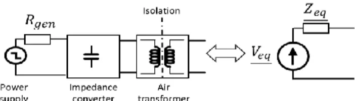
Considering that the optimized transformer acts as a bandpass filter, the first harmonic analysis allows to have a good estimation of the output power. This presumption has been validated thanks to a transient analysis showing a maximum 10% error with the first order approximation as shown in table 3. The generator is modeled by a resistive equivalent source. The maximum power that may be transferred can be calculated with a proper impedance matching and a Thevenin equivalent circuit composed by the generator, the primary impedance converter and the transformer as modeled in Fig. 4.
Fig. 2 Conversion chain based on a coreless transformer.
Fig. 4 Thevenin equivalent circuit of the first part of the conversion chain
For a given source and a given transformer, the values of 𝑍𝑒𝑞and 𝑉𝑒𝑞 are not affected by the load or the secondary impedance converter 𝐶2, which mean that the equivalent model of the source is only dependent of value of 𝐶1.
This equivalent source can provide a limited power level to the secondary converter and the load 𝐶2 and 𝑅𝑙 which must be chosen to absorb as much power as possible from the upstream conversion chain. Thanks to the maximum power theorem we can estimate the maximum power deliverable by the equivalent source constituted by 𝑍𝑒𝑞and 𝑉𝑒𝑞 to the secondary. The maximum power transmission is obtained when the load modeled by 𝑍𝑙𝑜𝑎𝑑, is perfectly matched to the source (1).
𝑍𝑒𝑞∗= 𝑍𝑙𝑜𝑎𝑑. (1)
When (1) is respected, the maximum power transmitted to the secondary 𝑃𝑚𝑎𝑥 can expresses with 𝑍𝑒𝑞and 𝑉𝑒𝑞 regardless of the load and the secondary impedance converter.
𝑃𝑚𝑎𝑥(𝐶1) =
𝑉𝑒𝑞2(𝐶1)
4 ∙ 𝑅𝑒 (𝑍𝑒𝑞(𝐶1)) (2) Therefore 𝐶1 can then be chosen by solving (3) in order to maximize the power transmitted.
𝜕𝑃𝑚𝑎𝑥
𝜕𝐶1 = 0 (3)
The load 𝑅𝑙 associated with the secondary impedance converter 𝐶2 are then chosen in order to respect (1).
For ease of reading, these shorted variables will be used.
𝑍𝐿1 = 𝐿𝑚𝜔 + 𝐿𝑒1𝜔
𝑍𝐿𝑚 = 𝐿𝑚𝜔 𝑅𝑔1= 𝑅𝑔𝑒𝑛+ 𝑅1
For a serial primary compensation, SS and SP topologies, the optimal value of C1 is given by
𝐶1= 1 𝑍𝐿1𝜔
(4) For a parallel primary compensation, PP & PS topologies the optimal value of C1 is given by
𝐶1= 𝑍𝐿1 (𝑍𝐿12+𝑅1 𝑅2𝑍𝐿𝑚 2+ 𝑅 12)𝜔 (5) If we consider that the power supply provides an rms tension 𝑉𝑖𝑛, for SS and SP topologies the maximum power given by the equivalent source is:
𝑃𝑚= 𝑉𝑖𝑛
2 4𝑅𝑔1(1 +𝑅𝑍2𝑅𝑔1
𝐿𝑚
2) (6)
For PP and PS topologies, the maximum power becomes: 𝑃𝑚 = 𝑉𝑖𝑛2((𝑍 𝐿1 2+ 𝑅 12) +𝑅𝑅1 2𝑍𝐿𝑚 2) 4 [A4R2 𝑍𝐿𝑚2 + A²(𝑅1+ 𝑅𝑔1) + 𝑍𝐿𝑚 2𝑅1 𝑅2𝑅𝑔1] Where 𝐴² = 𝑍𝐿12+ 𝑅1𝑅𝑔1 (7)
The secondary compensation is then calculated in order to match the equivalent source. When a rectifier is used, it can be modeled with the first harmonic approximation, as shown in Fig. 5.
Fig. 5 Secondary impedance converter equivalent model.
In order to match the equivalent source, for a serial secondary compensation, SS and PS topologies the load and the impedance converter are given by
𝐶2=
1 −𝐼𝑚(𝑍𝑒𝑞) ∙ 𝜔
𝑅𝑙 = 𝑅𝑒(𝑍𝑒𝑞) (10)
For a parallel secondary compensation, SP and PP topologies the optimal values become
𝑅𝑙 = 𝑅𝑒(𝑍𝑒𝑞) ∙ (1 + (𝐼𝑚(𝑍𝑒𝑞) 𝑅𝑒(𝑍𝑒𝑞)) 2 ) (11) 𝐶2= 𝐼𝑚(𝑍𝑒𝑞) 𝜔 ∗ (𝑅𝑒(𝑍𝑒𝑞)2+ 𝐼𝑚(𝑍 𝑒𝑞)²) (12)
A combination between a parallel and a series compensation allows to have more flexibility regarding the optimal load.
Topology choice
The choice of the secondary compensation has no effect on the output power available as expressed by (2). It can be proven mathematically by comparing (6) and (7) that serial compensation for the primary side will be able to provide more power if the condition given by (13) is respected.
𝑅𝑔𝑒𝑛2< 𝑍 𝐿12 +𝑅𝑅1
2𝑍𝐿𝑚
2+ 𝑅
12 (13)
In most cases the power source is less resistive than the transformer, making the serial compensation for the primary the ideal choice for maximizing the power transferred.
In addition, the primary compensation has a clear effect on the current drown by the converter. On the one hand, the serial compensation avoids DC current passing through the transformer. On the other hand, when the converter is supplied by a square source, the voltage transient can create a substantial current peak in the parasitic and compensation capacitances. As a result, this may stress the source and increase drastically the losses in the converter, and, as a consequence lower the efficiency of the whole conversion chain. This current peak is due to the low impedance seen by the source at high frequency.
In the case of a parallel primary compensation the power source will be directly connected to the capacitance which will drain high frequency currents. Nevertheless, in the case of a serial primary the high frequency currents are stopped by the primary 𝐿𝑒1 and 𝐿𝑚, although it may pass though the interwinding capacitance 𝐶𝑝1.
This phenomenon can be avoided by using a sinusoidal source, or by adding shock inductors between the generator and the impedance converter, this would increase the impedance seen by the power source at high frequency. However the primary compensation capacitance would have to be changed accordingly and the output power would be affected by the losses in the added inductors.
Finally it must be pointed out that the sensibility over the choice of the impedance converter’s elements values changes according to the generator, transformer and the topology chosen. For example, for the primary impedance converter unlike the parallel compensation the optimal value of 𝐶1 for a serial compensation is independent of the coupling and 𝑅1 and 𝑅2. It can be also noted that the parallel primary capacitor has no effect as long as the generator used presents a negligible impedance in front of the one of the compensated transformer. The sensibility analysis allows to choose the topology in order to adapt the converter to the physical constraint and to focus the attention on the choice of the key components.
Transformer characterization
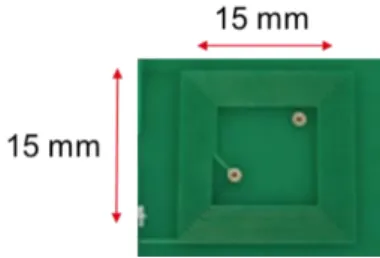
To validate the proposed methodology, the PCB coreless transformer shown in Fig 6 has been used.
The primary as well as the secondary have been made with 18 square turns on two layers. The copper tracks are 17µm thick and 200 µm width and 150 µm isolation between each turn. The primary and secondary are separated with 710 µm of FR4.
Fig. 6 Transformer used for experimental validation of the proposed design methodology
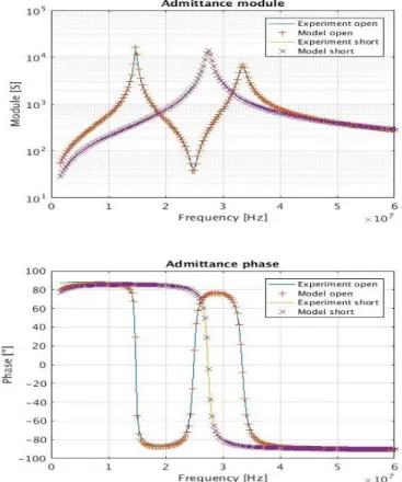
In order to perfectly tune the matching elements the transformer used has been measured with a Keysight E4990A impedance analyzer.
𝐶12. is determined by shorting the primary and the secondary and measuring the impedance between the two.
An algorithm has then been applied in order to match the model with the measurement of the impedance of the transformer with open and short secondary. The open secondary measurement presents two peaks, which is a direct consequence of the bifurcation phenomena [4]. In our case, the first peak is due to the resonating RLC circuit composed of 𝐶1, 𝐿𝑒1, 𝐿𝑚 then the second peak is mainly due to the RLC composed of 𝐶1, 𝐶2, 𝐶12, 𝐿𝑒1, 𝐿𝑒2.
To consider the skin effect, the resistors have been modeled by 𝑅 = 𝑅0+ 𝑅𝑠𝑘𝑖𝑛∙ √𝑓. The estimated values can be found in Table 1. The real part of the impedance measured being several decades lower than the imaginary part at the working frequency, the resistive values are difficult to measure. The measurement of the resistive parts would be improved by tuning the resonant devices at the working frequency.
Keeping in mind that the current crowding effect is linked to the current passing through the magnetizing inductor, meaning that the values of the model’s elements are dependent on the source and the load.
Fig. 7 Results of the matching algorithm between the model and the measurements.
Element Value Unit
𝑅1 1,5+0,002√𝑓 Ω 𝑅2 1,5+0,002√𝑓 Ω 𝐿𝑒1 1,3 µH 𝐿𝑒2 2,53 µH 𝐿𝑚 4,25 µH 𝐶1 11 pF 𝐶2 11 pF 𝐶12 8,2 pF
Table.1 Estimated values for the model (Fig.1)
Experimental validation of the
proposed method.
Fig. 8 Experimental set up
To compare the compensations methods, a square wave generator has intentionally been used as drawn in fig. 8.
To ensure that the good impedance converters and load have been placed, the impedance of the loaded compensated transformer has been measured and then compared to the simulation. For each topology the calculated capacitance has been welded and adjusted thanks to a comparison with the simulation. During the tests, the conversion chain has been supplied with an EPC9004 development board under 1MHz. The capacitances and load used are given in Table 2.
SS SP PS PP unit
𝐶1 4.56 4.56 2.84 2.84 nF 𝐶2 3.99 0.156 7.16 6.72 nF 𝑅𝑙 197 205 5.66 92.8 Ω Table 2 Values calculated and used for the compensation with each topology
The first harmonic analytic analysis has been validated with a transient simulation and experimental measurements (table 3).
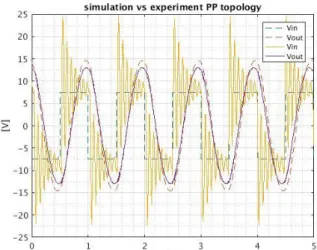
An error lower than 7% has been noticed between the simulations. The discrepancy is due to the harmonics neglected in the analytical analysis. The compensated transformer act as a bandpass filter. Unlike the SS topology, the PP topology allow a part of the current to pass through the capacitor without passing through the resistors 𝑅1 and 𝑅2, increasing the quality factor of the filter formed. As a result, the SS topology allows more harmonics to pass through the transformer and the output waveform display stronger harmonics than the others topologies as seen on Fig 9 and 10 The experimental measurements are showing an output power up to 33% lower. This discordance is due to a mismeasurement of the coils resistors, and the lack of current crowding simulation.
Table 3 Output power and error vs first harmonic simulation for first harmonic simulation (proposed methodology), circuit simulation and measured for each topology.
Fig. 9 Experiment and numerical simulation (dashed) of the SS topology
Fig. 10 Experiment and numerical simulation (dashed) of the PP topology
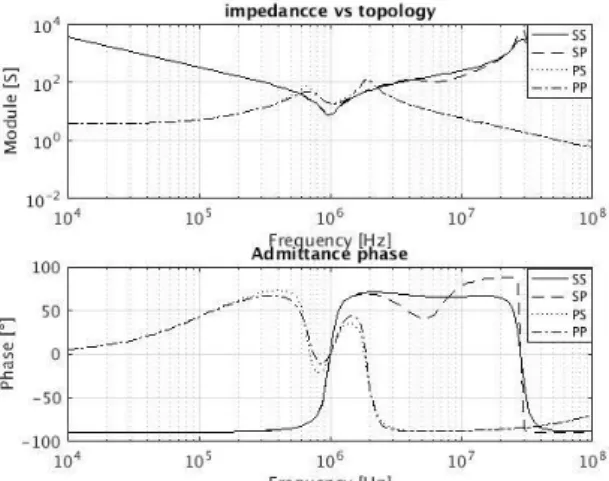
The measure of the current passing through the primary has been done on the characterized and compensated transformer, as expected the normalized frequency spectrum (Fig 11) present for the PS topology a richer frequency spectrum at 10 MHz. The transformer with a parallel compensation at the primary possesses a much lower input impedance at high frequency as shown on Fig. 12. These harmonics in the current absorbed by the transformer are increasing the losses within the power chin without increasing the output power. With a parallel compensation the strong current peaks induced are creating strong oscillation of the power source as seen on Fig. 10.
Fig. 11 frequency spectrum of the current measured
SS SP PS PP First harmonic simulation 3.02 3.02 1.17 1.17 W Transient simulation 3.30 3.00 1.12 1.16 W 6.6 0.7 4 0.8 % Experiment 2.02 2.02 0.85 0.99 W 33 33 27 15 %
Fig. 12 Impedance seen by the power source obtained by simulation with the converter tuned at 1MHz
Conclusion
For a given transformer the maximum transferable power can be calculated. In order to reach this power an addition of two impedance converters is required. The choice of compensation used for the primary side impact the output power, but also the current draw by the system. Knowing the transformer and the source used, the optimal compensation can be calculated thought equation (13).
Using the proposed methodology and models, 2W has been transferred through a 2.25cm² coreless transformer under 1MHz, with a parasitic capacitance between the primary and secondary lower than 10pF.
Knowing the maximum output power delivered by a given transformer, an optimization can easily be done during the earliest stages of the transformer design can be easily done.
Since we are using a resonant compensation, the slightest variation of several parameters can drastically affects the power delivered. These variations can be created by production fluctuation, temperature changes, coupling with surrounding materials or by the current crowding
phenomena. A sensibility analysis seems to be a key element in developing a closed loop approach to industrial production and will be investigated in our future works.
R
eferences
[1] Y. Wanderoild, D. Bergogne, and H. Razik, “High Frequency, High Temperature designed DC/DC Coreless Converter for GaN Gate Drivers,” PCIM Eur. 2016, 2016.
[2] D. Bergogne et al., “Integrated coreless transformer for high temperatures design and evaluation,” in 2013 15th European Conference on Power Electronics and Applications (EPE), 2013, pp. 1–8.
[3] A. F. Witulski, “Introduction to modeling of transformers and coupled inductors,” IEEE
Trans. Power Electron., vol. 10, no. 3, pp. 349–
357, May 1995.
[4] C.-S. Wang, G. A. Covic, and O. H. Stielau, “Power transfer capability and bifurcation phenomena of loosely coupled inductive power transfer systems,” IEEE Trans. Ind.
Electron., vol. 51, no. 1, pp. 148–157, Feb.
2004.
[5] C. Auvigne, P. Germano, Y. Perriard, and D. Ladas, “About tuning capacitors in inductive coupled power transfer systems,” in 2013 15th
European Conference on Power Electronics and Applications (EPE), 2013, pp. 1–10.
[6] H. H. Wu, A. P. Hu, S. C. Malpas, and D. M. Budgett, “Determining optimal tuning capacitor values of TET system for achieving maximum power transfer,” Electron. Lett., vol. 45, no. 9, pp. 448–449, Apr. 2009.
[7] M. E. Halpern and D. C. Ng, “Optimal Tuning of Inductive Wireless Power Links: Limits of Performance,” IEEE Trans. Circuits Syst.
Regul. Pap., vol. 62, no. 3, pp. 725–732, Mar.