The MIT Faculty has made this article openly available.
Please share
how this access benefits you. Your story matters.
Citation
Palacios, T., A. Hsu, and Han Wang. “Applications of graphene
devices in RF communications.” Communications Magazine, IEEE
48.6 (2010): 122-128. © 2010, IEEE
As Published
http://dx.doi.org/10.1109/mcom.2010.5473873
Publisher
Institute of Electrical and Electronics Engineers
Version
Final published version
Citable link
http://hdl.handle.net/1721.1/61760
Terms of Use
Article is made available in accordance with the publisher's
policy and may be subject to US copyright law. Please refer to the
publisher's site for terms of use.
I
NTRODUCTION
In 2004 scientists from the University of Manch-ester isolated graphene, a one-atom-thick layer of carbon atoms arranged in a honeycomb lattice through sp2bonding (Fig. 1) [1]. Considered for many years an impossible goal, the isolation of graphene triggered a revolution not only among condensed matter physicists but also among chemists and engineers, eager to take advantage of its unique properties [2, 3].
The symmetry of its honeycomb lattice struc-ture confers to graphene very unique transport properties [4]. For example, the carriers in graphene lose their effective mass and can be described by a Dirac-like equation instead of by the Schrödinger equation used in traditional semiconductors. This very low effective mass is responsible for a very high electron and hole mobility in excess of 200,000 cm2/Vs at T = 5 K [5] and in excess of 100,000 cm2/Vs at T = 240 K in suspended graphene [6], the highest ever reported for any semiconductor. Second, graphene is a zero-bandgap material where the conduction and valence bands touch each other at a point called the Dirac point. In addition to this zero bandgap, the density of states in graphene is zero at the Dirac point and increas-es linearly for energiincreas-es above and below it, which allows for carrier modulation. Third, the carriers in graphene are confined to a layer that is only one atom thick. This allows unprecedented elec-trostatic confinement, and also makes graphene extremely flexible and transparent.
These unique properties of graphene have motivated intense work among physicists and engineers who have seen in this material new opportunities to improve digital and radio fre-quency (RF) electronics, advanced sensors, transparent electronics, low-power switches, solar cells, and even battery energy storage. In this article we review some of the recent progress made in the use of graphene devices for commu-nication applications. The next section discusses the various growth techniques currently used to synthesize graphene, and we then introduce the basic fabrication technology common to many graphene devices. We then describe several graphene devices with the potential to impact future communication systems. In particular, we summarize the current effort on graphene low noise amplifiers, graphene nonlinear electronics, and focus on the use of graphene in RF elec-tromechanical resonators and switches. The final section offers some conclusions and future prospects of this amazing new material.
G
RAPHENE
G
ROWTH
Graphene was first discovered through the suc-cessive peeling of highly oriented pyrolytic graphite (HOPG) using scotch tape [1]. This amazingly simple method, also known as
mechanical exfoliation, has been effective at
pro-ducing graphene flakes 20–1000 μm in length, and has been the primary source material for most papers reporting graphene’s extraordinary physical and electronic properties. Unfortunate-ly, while these flakes have generated impressive performance, working with them involves con-suming effort to locate and identify single-layer flakes. Furthermore, electron beam lithography is necessary to pattern graphene transistors in these randomly arranged flakes, and it usually has a throughput of only a couple of transistors per sample.
Therefore, extensive research and interest have focused on developing methods for large area synthesis of graphene. The two most com-mon methods are silicon carbide (SiC) sublima-tion and chemical vapor deposisublima-tion (CVD). The first method is the process of heating silicon car-bide substrates under vacuum [7]. By heating up these substrates to about 1400°C, the silicon at the surface sublimates, leaving behind carbon
A
BSTRACT
Graphene, a one-atom-thick layer of carbon atoms arranged in a honeycomb lattice, has recently attracted great interest among physicists and engineers. The combination of the unique properties of graphene with new device concepts and nanotechnology can overcome some of the main limitations of traditional radio frequency electronics in terms of maximum frequency, lin-earity, and power dissipation. In this article we review the current status of research on graphene-based electronic devices for RF appli-cations. The future challenges facing this rising technology and its feasibility for a new genera-tion of applicagenera-tions in RF communicagenera-tions and circuits are also discussed.
N
ANO
-T
ECHNOLOGY IN
C
OMMUNICATIONS
Tomás Palacios, Allen Hsu, and Han Wang, Massachusetts Institute of Technology
Applications of Graphene Devices in
RF Communications
IEEE Communications Magazine • June 2010 123 that forms thin crystalline graphene sheets. By
controlling the crystal orientation of the SiC, one can control the number and mobility of graphene layers. The growth on the Si-face of SiC renders a few-layer graphene sheet with mobilities around 1500 cm2/Vs, while the growth on the C-face results in much thicker multilayer graphene with mobilities as high as 200,000 cm2/Vs. The screening of charged impurities by the outermost graphene layers is believed to be responsible for the very high mobility reported in the thick graphene grown on C-face SiC. In spite of the higher mobility of graphene grown on C-face, Si-face is typically used for RF devices due to the much higher carrier modulation resulting from the thinner graphene layer [8]. Unfortunately, the high cost and relatively small size of available SiC wafers (up to 4” in diame-ter) does not make this process amenable to large wafer scale processing.
Conversely, CVD graphene can be grown on arbitrary sized wafers coated with thin film cata-lysts. These metal catalysts serve to help decom-pose hydrocarbon gases into elemental carbon and hydrogen, and provide a substrate for car-bon deposition. The observation of carcar-bon depo-sitions on metal catalysts has been known for many years due to their reduction of catalytic efficiency of nickel. It is only with the discovery of graphene that this effect has been harnessed for large area synthesis. The two most common metal catalysts used today are nickel and copper, each of which can be deposited as a thin film or rolled into thin foils. Initial work focused on ambient pressure CVD (AP-CVD) on nickel films [9, 10]. Carbon deposited on the surface of the catalyst diffuses into the bulk, creating a solid solution of metal and carbon. Due to the change in solubility with respect to temperature, carbon begins to precipitate out of solution as the sample is cooled down. Through careful con-trol of the cooling rates, the surface coverage of single and bilayer graphene can be controlled, yielding > 80 percent coverage. Recently it has been shown that due to the lower bulk solubility of carbon in copper, the reaction of graphene on copper is surface limited, producing almost com-plete coverage of single-layer graphene [11]. Furthermore, copper growth is done with low-pressure CVD (LP-CVD), and thus allows for higher throughput growth and conserves on source materials.
As with HOPG graphene, CVD grown graphene needs to be transferred onto an insu-lating substrate before processing. This is done by spin coating a thin polymer layer such as PMMA on top of the graphene followed by chemical etching of the catalyst — thus freeing the graphene/PMMA film from the substrate (Figs. 2 and 3a). The film can then be trans-ferred to any arbitrary substrate. The PMMA is then removed using solvents and forming gas annealing to burn off any organic residue. This process has no fundamental limitations on size and has already been demonstrated on 4-in wafers. Observed mobilities are also on the same order as SiC of 1000–2500 cm2/Vs. Most recent work has been focused on optimizing the catalyst and growth conditions to achieve the highest quality and largest grain sized graphene.
Fur-thermore, transferless processes and direct growth on insulating substrates similar to SiC are being investigated to further simplify the growth and fabrication process.
G
RAPHENE
F
ABRICATION
T
ECHNOLOGY
Although graphene shares many of its outstand-ing properties with carbon nanotubes, graphene devices are strongly preferred from a commer-cial point of view because their fabrication is very similar to traditional planar wafer-size Si processing. Devices are patterned using standard photolithography tools or electron-beam lithog-raphy. Metal contacts are deposited through lift-off, and graphene is subsequently etched with oxygen plasma. Finally, a gate dielectric is deposited and the gate metal is patterned (Fig. 3b). Most of the fabrication technology mirrors all the work done on carbon nanotube field effect transistors (CNT-FETs) in terms of selec-tion of ohmic metals, gate dielectrics, and so on. However, there are four main issues for graphene fabrication that still require optimiza-tion: substrate selection, contact resistance, gate dielectric deposition, and band gap engineering.
Every atom in a graphene film is at the sur-face and strongly interacts with the surrounding environment, which opens numerous opportuni-ties for new device concepts, but also new sources of performance degradation. So far the most dominant mechanism for mobility degrada-tion in graphene is charged impurities. There-fore, much work has been dedicated to studying various high-k dielectric materials and substrates to screen the effects of any charged impurities and reduce surface phonon effects. By carefully controlling the graphene-substrate interface, mobilities as high as 20,000 cm2/Vs have been demonstrated. In spite of some partial success in identifying suitable substrates, more work is needed in this area as the reported mobilities are still far from the record mobility recorded in suspended graphene, where the substrate under-neath the graphene film was etched away [5]. The lack of substrate in these measurements prevents any degradation through surface
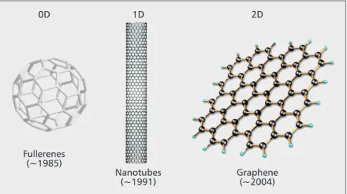
vibra-Figure 1. Diagram of different low-dimensional carbon structures and the year of their discovery/isolation. 0D 1D 2D Fullerenes (~1985) Nanotubes (~1991) Graphene (~2004)
tions (phonons) or nearby charged impurities, both of which greatly reduce graphene’s intrinsic properties. However, most practical applications require that a substrate allows for proper heat dissipation; therefore, the choice of substrate and its interaction with graphene are of utmost importance.
A second important processing issue in graphene devices is to optimize the metallization for reducing contact resistances. Most work has been done on matching work functions of graphite and the metal. The most common metal combinations are Cr/Au, Ti/Pt, and Ti/Pd/Au. Based on experiments done in our laboratory, Cr/Au contacts give contact resistances in the range 1 × 10⁻⁴– 2 × 10⁻⁴ohm.cm2. Ti/Pt gives similar contact resistance as Cr/Au contacts. Ti/Pd/Au contacts give contact resistances in the range 0.5 × 10⁻⁴– 1 × 10⁻⁴ohm.cm2. However, there is still no consensus as to which one pro-vides the lowest contact resistance. Furthermore, since graphene is so easily doped by its environ-ment, metal on graphene may end up doping the underlying graphene, creating a potential barrier into the undoped graphene channel. This increased resistance is detrimental towards high-speed operation due to the increased RC time to charge and discharge all of the capacitances.
One of the most difficult problems with graphene processing has been finding the appro-priate gate dielectric material. Atomic layer deposition (ALD) is the most commonly used deposition method due to the accurate control of the layer thickness that it allows. Unfortu-nately, ALD relies upon alternating pulses of water and precursor materials. Graphene is hydrophobic and thus the deposition of high quality pinhole-free ALD is very difficult. Vari-ous approaches have been attempted utilizing chemical functionalization with NO2, aluminum
oxidation, or seed layers to provide a template for ALD that does not reduce the mobility of the carriers in graphene. Recently, impressive results in mobility have been demonstrated through non-covalent bonding of polymers on graphene to serve as a thin buffered layer [12].
Finally, there is growing interest in bandgap engineering of graphene. Unlike conventional semiconductors such as silicon, which contain a bandgap, graphene is a zero-bandgap material and has ON/OFF ratios around 5–10, thus limit-ing its effectiveness for digital applications. Much work has been focused on generating a bandgap of up to 500 meV through 1-D quan-tum confinement of graphene nanoribbons (GNR) or through strain induced substrate interactions. So far, GNR have demonstrated moderate band gaps that have translated to much higher ON/OFF ratios [13], however the fabrication of these GNR transistors is very chal-lenging. Electron-beam lithography is limited to feature sizes around 10–20 nm. However, to gen-erate an appropriate sized band gap requires dimensions on the order of <10 nm. Further-more, sidewall roughness also limits the mobility of these transistors due to edge state scattering. An alternative approach to open a bandgap is by applying vertical electric fields in bilayer graphene [14]. Although this method has been successful in opening optical bandgaps (100–200 meV), the electrical bandgap has been much smaller than expected (<20 meV) and more work is needed to understand the full potential of this technology.
L
OW
N
OISE
A
MPLIFIERS
Graphene is uniquely suited for high frequency low noise amplifiers. Its extremely high mobility offers the potential of ultra low source-to-drain
Figure 2. Main steps in the CVD growth and transfer of graphene.
p-type Si 300 nm SiO2 Ni Ni deposition 500nm Ni deposited on SiO2/ Si substrate by e-beam evaporation p-type Si 300 nm SiO2 Ni Annealing of Ni 10-20min at 900-1000C 600 sccm Ar 500 sccm H2 p-type Si 300 nm SiO2 Ni Graphene CVD growth 5-10min at 1000C 5-25 sccm CH4 1500 sccm H2 p-type Si 300 nm SiO2 Ni Graphene PMMA Arbitrary substrate Graphene PMMA Arbitrary substrate PMMA Graphene
Ni etching Transfer PMMA removal by acetone
Ni etched by aqueous HCI (~3% vol)
Graphene is uniquely suited for high frequency low noise
amplifiers. Its extremely high mobility offers the potential of ultra low
source-to-drain resistances, extremely
high current densities, and high efficiency operation.
IEEE Communications Magazine • June 2010 125 resistances, extremely high current densities, and
high efficiency operation. In addition, the unprecedented carrier confinement allowed by its one-atom thickness minimizes short channel effects and opens the door to ultra high frequen-cy operation.
The first graphene FET (GFET), reported in 2004, was fabricated on an HOPG graphene flake deposited on top of a SiO2/Si substrate [1]. The 300 nm thick SiO2layer deposited between the Si wafer and the graphene layer serves two different functions. First, its thickness was opti-mized to maximize the optical contrast between the graphene flake and the substrate in order to see the flake. Second, the SiO2layer served as gate dielectric. However, due to the large thick-ness of the SiO2layer, the device transconduc-tance was very low, severely degrading the device properties. Lemme et al. demonstrated in 2007 the first top-gated graphene transistor [15]. In this device, a thin SiO2layer was used as gate dielectric. Although the use of a top-gate allowed much higher gate capacitance and modulation capability, the SiO2gate dielectric used in this demonstration caused a seven-fold reduction in the electron and hole mobility of the graphene layer.
The last few years have seen a fast increase in the frequency performance of graphene transistors. For example, Moon et al. from HRL reported on the fabrication of GFETs grown on SiC substrates with an fT= 4.2 GHz and an fmaxof 14 GHz in self-aligned devices with a gate length of 1 μm [16]. A record power gain cut-off frequency (fmax) value of 14 GHz was reported for these devices. Y.M Lin from IBM reported non-self aligned devices fabricat-ed on graphene flakes with an intrinsic fTof 100 GHz [17]. To reduce the access resistances in these non-self-aligned devices, a substrate voltage was applied to induce carriers in the access regions.
In spite of the significant recent progress, there are still several issues that need to be overcome in order to use graphene as a low noise amplifier. First, the field effect mobility of graphene top-gated transistors, typically below 2000 cm2/Vs, is still many orders of mag-nitude lower than the mobility measured in sus-pended graphene samples. Also, the different surface functionalization methods used to deposit the gate dielectric on top of graphene are not completely reproducible. In addition, the lack of a bandgap reduces the ON-OFF modulation to a factor of 10, in the best case. This low modulation significantly reduces the device efficiency. Finally, the lack of a bandgap and the ambipolar transport increases the out-put conductance of these devices, which typical-ly do not show current saturation. This high output conductance severely limits their power gain performance.
To improve the ON-OFF ratio and to increase the efficiency of future graphene amplifiers, several groups are trying to induce a bandgap in graphene as discussed in the pre-vious section. However, each of the existing methods have their limitations either in fabri-cation or due to edge roughness of nanorib-bons.
A
MBIPOLAR
N
ONLINEAR
E
LECTRONICS
One of the most intriguing properties of graphene is its ambipolar transport [4]. In graphene ambipolar transistors, the drain cur-rent is based on hole conduction for gate-to-source voltages below the minimum conduction point voltage (VG,min), while at higher voltages electron conduction dominates, as shown in Fig. 4a. Ambipolar transport in graphene together with its high mobility truly distinguishes graphene from other semiconductor materials and allows completely new nonlinear devices for radio frequency (RF) and mixed-signal applica-tions, such as full wave rectifiers, frequency dou-blers, and mixers.
The V shaped current-voltage (I-V) transfer characteristic of graphene ambipolar transistors [4, 18] closely resembles that of an ideal full-wave rectifier (Figs. 4b and 4c). With a single graphene device it is therefore possible to realize full-wave rectification with zero-volt threshold voltage, something that would require a full bridge circuit with four diodes made of conven-tional semiconductors or an operaconven-tional amplifi-er for zamplifi-ero-volt rectification.
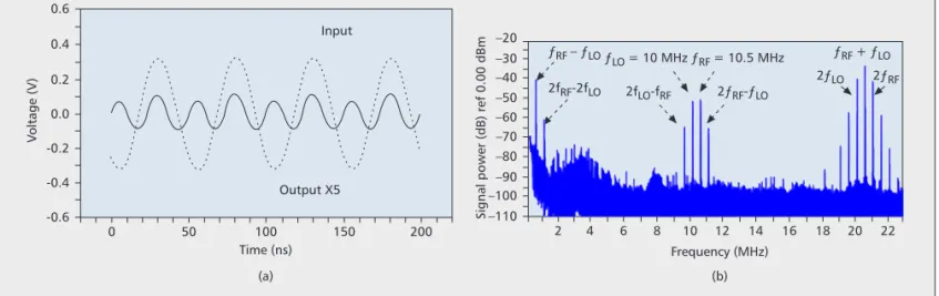
Graphene ambipolar transistors can also be used for frequency doubling [18], by biasing the gate to the minimum conduction point and superimposing a sinusoidal input signal to the gate (Fig. 4d). Electrons and holes conduct in alternative half cycles to produce an output sig-nal at the drain, whose fundamental frequency is twice that of the input. Figure 5a shows the experimental demonstration of this concept based on CVD grown graphene with an input frequency of 20 MHz and an output frequency of 40 MHz. This frequency doubler device shows high spectral purity in the output RF signal, where 93 percent of the output RF energy is at the fundamental frequency (40 MHz). Measure-ments at a lower input frequency (100 Hz) demonstrated similar spectral purity, confirming that the high spectral purity at the output is due to the sublinear IDS-VGScharacteristics, not to parasitic capacitances. This is the first time fre-quency doubling is realized with just a single transistor device and with high spectral purity at the output without any filtering elements.
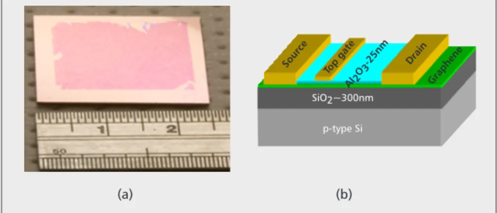
Figure 3. a) Optical micrograph of a CVD-grown graphene layer transferred to a Si substrate (courtesy of Jing Kong's lab at MIT); b) cross-sectional structure of a graphene field effect transistor. The p-type Si substrate is often used as a bottom gate to the device.
Source AI2 O 3-25nm Gra phene SiO2~300nm p-type Si (a) (b) Drain Top gate
GFETs can also act as a nonlinear compo-nent for frequency mixing. The symmetrical transfer characteristics of GFETs usually show a very significant quadratic component (Fig. 4a); hence, these devices can be used as excellent RF mixers. Assuming that the transfer characteris-tics of the GFET are completely symmetric, and infinitely differentiable, we can then describe the drain current as
ID= a0+ a2(VGS– VG,min)2
+ a4(VGS– VG,min)4+ …, (1) where VG,minis gate voltage at the minimum conduction point. a0, a2, a4, … are constants. From this expression, for ideal GFETs with sym-metric transfer characteristics and biased at the
minimum conduction point, no odd-order inter-modulation distortions should appear at the out-put, and all the output power is coupled to the difference and sum frequency, and other even-order terms. Therefore odd-even-order intermodula-tions, which are often present in conventional unipolar mixers and are harmful to circuit oper-ations [19], can be significantly suppressed in GFET mixers.
Figure 5b shows the power spectrum at the output of a graphene mixer. If two signals, an RF input signal and a local oscillator (LO) signal with frequencies fRF= 10.5 MHz and fLO= 10 MHz, are introduced to the gate, the GFET mixes them to generate output signals with a fre-quency equal to the sum (fRF + fLO = 20.5 MHz) and difference (fRF– fLO= 500 kHz) at
Figure 4. a) Transfer characteristic of a typical ambipolar G-FETs fabricated in the Palacios' lab at MIT; b) circuit diagram of a full-wave rectifier made with conventional diodes; c) transfer characteristics of the full-full-wave rectifier circuit shown in b). Diodes with zero threshold voltage are required to achieve this ideal behavior; d) graphene-based circuit for frequency multiplication of the input signal
Vin. With the device biased at the minimum conduction point, electrons (e–), and holes (h+) conduct alternatively in neighboring
half-cycles of the output signal.
Gate voltage VGS (V) (a) (b) (c) (d) h+ current e- current -4 1.0 Drain-source current/ DS (mA) 0.8 1.2 1.4 1.6 1.8 2.0 -5 -3 -2 Minimum conduction point
-1 0 1 2 3 4 5 D S + -G Input Output e -Vin Vin +Vs R0 /DS VGS Vin Vg,min Vout Vout Load h+ e- h+
IEEE Communications Magazine • June 2010 127 the same time that the odd-order
intermodula-tion products are significantly suppressed. These new devices, a result of the unique transport properties of graphene, can potentially revolu-tionize the way many RF communication circuits are designed and can improve chip performance. Compared to conventional Si and III-V elec-tronics, ambipolar graphene electronics have many advantages. The higher mobility of graphene allows higher operating frequency for frequency doubling and mixer applications. In addition, ambipolar devices can significantly reduce the number of transistors needed in these applications. Simpler circuits mean less power consumption and smaller chip area. In addition, graphene is also an ideal material for flexible electronics. Graphene grown by CVD can be transferred to arbitrary substrates, including transparent and elastic substrates. Furthermore, the two-dimensional geometry, in combination with the excellent chemical and thermal stability of graphene make fabrication of graphene cir-cuits fully compatible and integrable with silicon technology, which is the mainstream of the semi-conductor industry.
To achieve the expected high frequency per-formance, the device geometries and technology need to be optimized. The current frequency performance of graphene mixers is limited to tens of megahertz in this experiment due to the parasitic capacitances and resistances. fTcan be calculated by using the expression
In our device gm= 5.5 mS/mm, as obtained from the slope of the IDS-VGScurve. Capacitance-volt-age (CV) measurements show a gate capacitance of 4.5 pF/mm in this device. This leads to a cal-culated fTof about 190 MHz for these devices. Higher frequency performance can be achieved by shrinking the gate length and gate oxide thickness in the device. As a first order estima-tion, using a 1/L2Gdependence for fT, the maxi-mum frequency of these devices will be in the
gigahertz range for gate lengths less than 1 μm, and exceeding 100 GHz for gate lengths of 60 nm. Much higher frequencies would be possible in devices with mobilities above 1000 cm2/Vs.
G
RAPHENE
R
ESONATORS AND
RF S
WITCHES
Numerous communication systems rely on elec-tromechanical devices, such as filters, resonators, and RF switches. The miniaturization of these devices will strongly affect the development of future communication systems. The ultimate limit to this miniaturization is represented by graphene electromechanical devices, which are only one atom thick. In fact, its enormous stiff-ness and low density make graphene the ideal material for these kinds of devices.
The first electromechanical devices ever demonstrated in graphene were nanomechanical resonators. In 2009 Chen et al. fabricated mono-layer graphene nanomechanical resonators with operating frequencies in the 50–80 MHz fre-quency range [20]. These devices showed quality factors of ~1 × 10⁴at low temperatures (5 K). It has been predicted that graphene’s ability to withstand ultrahigh strains, up to ~25 percent in nanoindentation experiments, will allow increas-ing the resonance frequency of these devices above the gigahertz range while maintaining a robust signal level.
Graphene electromechanical switches have also been demonstrated recently. Milaninia et al. [21] developed a switch comprising two polycrys-talline graphene films grown by CVD. The top film is pulled into contact with the bottom one by applying a voltage of 5 V between the layers, and the contact is broken after removing the voltage due to restoring mechanical forces. In the ON state, more than 7 kA/cm2of current can flow through the switch. Although the device performance suffers from a relatively large con-tact resistance, it is expected that the graphene-graphene contact will be more robust than the traditional metal-metal contact, which will
signif-f g C T m G = 2π .
Figure 5. a) Experimental demonstration of a graphene frequency multiplier with input signal at 20 MHz and output signal at 40 MHz. Frequency doubling is clearly achieved. The output signal shows high spectral purity and low noise. b) Power spectra at the output of a graphene ambipolar mixer with input signals at 10 and 10.5 MHz. Due to the symmetric character of the transfer characteristic of a graphene ambipolar device, the odd-order intermodulation products are attenuated with respect to the even-order ones.
Time (ns) 0 (a) (b) -0.4 V oltage (V) -0.6 -0.2 0.0 0.2 0.4 0.6 50 100 Input Output X5 150 200 Frequency (MHz) 2
Signal power (dB) ref 0.00 dBm –110
–100 –90 –80 –70 –60 –50 –40 –30 –20 4 6 8 ƒLO = 10 MHz 2fLO-fRF 2ƒLO 2ƒRF 2ƒRF-ƒLO 2fRF-2fLO ƒRF – ƒLO ƒ ƒRF + ƒLO RF = 10.5 MHz 10 12 14 16 18 20 22
icantly increase the reliability of future DC and RF switches.
C
ONCLUSIONS
, C
HALLENGES
,
AND
P
ROSPECTS
In summary, graphene is both quantitatively and qualitatively different from any other mate-rial conventionally used in electronic applica-tions. Not only does it have room temperature electron and hole mobilities more than 100 times higher than those of Si, as well as excel-lent mechanical properties, but also, its ambipo-lar transport properties, ultra thin and flexible structure, and electrostatic doping offer a new degree of freedom for the development of advanced electronic devices with many poten-tial applications in communications and RF electronics.
From the preliminary device results currently available, graphene offers great potential to impact RF communication electronics in areas as diverse as low noise amplifiers, frequency multipliers, mixers and resonators. However, in order to take advantage of the full potential of graphene devices, more basic research needs to be combined with improved material growth and device technology. A better understanding of parameters such as breakdown voltage, electron velocity, and saturation current is needed to allow a complete benchmark of this material and an evaluation of its potential performance. In addition, these new applications will have to overcome the limitations of graphene that arise from the lack of bandgap.
Once the growth and fabrication technology of these new devices matures, their integration with conventional Si electronics, and/or flexible and transparent substrates has the potential to transform communications. Advanced graphene devices could enable the introduction of advanced RF communication systems in a broad array of new applications. Graphene, the ulti-mate nano-ulti-material, is therefore in an excellent position to help RF communication systems become even more ubiquitous and versatile than they are today.
A
CKNOWLEDGMENTSThis work was partially supported by the GATE MURI program, monitored by Dr. Chagaan Baatar, and by the MIT/Army Institute for Sol-dier Nanotechnology.
R
EFERENCES[1] K. S. Novoselov et al., “Electric Field Effect in Atomically Thin Carbon Films,” Science, vol. 306, 2004, p. 666. [2] A. K. Geim and K. S. Novoselov, “The Rise of Graphene,”
Nature Materials, vol. 6, Mar. 2007, pp. 183–91. [3] A. K. Geim, “Graphene: Status and Prospects,” Science,
vol. 324, June 2009, pp. 1530–34.
[4] A. H. Neto et al., “The Electronic Properties of Graphene,” Rev. Modern Physics, vol. 81, 2009, p. 109. [5] K. Bolotin et al., “Ultrahigh Electron Mobility in Sus-pended Graphene,” Solid State Commun., vol. 146, June 2008, pp. 351–55.
[6] K. I. Bolotin et al., “Temperature-Dependent Transport in Suspended Graphene,” Physical Rev. Letters, vol. 101, 2008, article ID: 096802.
[7] C. Berger et al., “Electronic Confinement and Coherence in Patterned Epitaxial Graphene,” Science, vol. 312, 2006, p. 1191.
[8] J. S. Moon et al., “Epitaxial-Graphene RF Field-Effect Transistors on Si-Face 6H-SiC Substrates,” IEEE Electron Device Letters, vol. 30, 2009, pp. 650–52.
[9] A. Reina et al., “Large Area, Few-Layer Graphene Films on Arbitrary Substrates by Chemical Vapor Deposition,” Nano Letters, vol. 9, 2008, pp. 30–35.
[10] K. S. Kim et al., “Large-Scale Pattern Growth of Graphene Films for Stretchable Transparent Electrodes,” Nature, vol. 457, 2009, pp. 706–10.
[11] W. Cai et al., “Large Area Few-Layer Graphene/Graphite Films as Transparent Thin Conduct-ing Electrodes,” Applied Physics Letters, vol. 95, 2009, article ID: 123115.
[12] D. B. Farmer et al., “Utilization of a Buffered Dielectric to Achieve High Field-Effect Carrier Mobility in Graphene Transistors,” Nano Letters, vol. 9, Dec. 2009, pp. 4474–78.
[13] M. Y. Han et al., “Energy Band-Gap Engineering of Graphene Nanoribbons,” Physical Rev. Letters, vol. 98, 2007, article ID: 206805.
[14] Y. Zhang et al., “Direct Observation of a Widely Tun-able Bandgap in Bilayer Graphene,” Nature, vol. 459, pp. 820–23.
[15] M. Lemme et al., “A Graphene Field-Effect Device,” IEEE Electron Device Letters, vol. 28, 2007, pp. 282–84. [16] J. S. Moon et al., “Epitaxial-Graphene RF Field-Effect
Transistors on Si-Face 6H-SiC Substrates,” IEEE Electron Device Letters, vol. 30, 2009, pp. 650–52.
[17] Y.-M. Lin et al., “100-GHz Transistors from Wafer-Scale Epitaxial Graphene,” Science, vol. 327, no. 5966, p. 662. [18] H. Wang et al., “Graphene Frequency Multipliers,” IEEE
Electron Device Letters, vol. 30, 2009, pp. 547–49. [19] S.A. Maas, Microwave Mixers, Artech House, 1986. [20] C. Chen et al., “Performance of Monolayer Graphene
Nanomechanical Resonators with Electrical Readout,” Nature Nanotech., vol. 4, 2009, pp. 861–67.
[21] K. M. Milaninia et al., “All Graphene Electromechanical Switch Fabricated by Chemical Vapor Deposition,” Applied Physics Letters, vol. 95, 2009, article ID: 183105.
B
IOGRAPHIESTOMASPALACIOS(tpalacios@mit.edu) is an associate
profes-sor in the Department of Electrical Engineering and Com-puter Science at the Massachusetts Institute of Technology, where he leads the Advanced Semiconductor Materials and Devices Group. He received his Ph.D. in electrical engineer-ing from the University of California — Santa Barbara, and a B.Sc. degree from the Polytechnical University of Madrid, Spain. His research focuses on the development of new electronic devices to advance the fields of information technology, biosensors, and energy conversion. He is espe-cially interested in expanding the frequency performance of GaN transistors, and developing new devices and cir-cuits with graphene. His work has been recognized with multiple awards including the 2009 NSF CAREER Award, the 2009 ONR Young Investigator Award, the 2008 DARPA Young Faculty Award, the 2006 UCSB Lancaster Award, the Young Researcher Award at the 6th International Confer-ence on Nitride Semiconductors, the Best Student Paper Award at the 63rd IEEE Device Research Conference, and the European Prize Salva i Campillo. He has authored more than 100 contributions on advanced semiconductor devices in international journals and conferences (35 of them invit-ed), three book chapters, and eight patents.
ALLENHSUholds a Master’s degree in electrical engineering from Massachusetts Institute of Technology in 2008, and a Bachelor’s degree in electrical engineering from Princeton University in 2006. He is currently pursuing a Ph.D. in graphene electronics and optoelectronics at MIT.
HANWANGreceived his B.A. and M.Eng. degrees in electri-cal and information science, both with highest honors, from Cambridge University, England, in 2006 and 2007. He is currently pursuing his Ph.D. degree in electrical engineer-ing and computer science at MIT. He worked on modelengineer-ing and simulation of power electronic devices from 2006 to 2007 in Cambridge University. At MIT since 2008, he has been working on graphene-based electronics and GaN-based devices. His current research interest focuses on the development of graphene-based transistors for millimeter-wave applications and the search for novel graphene-based ambipolar devices for applications in nonlinear electronics. His work at MIT also includes GaN-based transistors for high frequency and high power applications.
Advanced graphene devices could enable the introduction of advanced RF com-munication systems in a broad array of new applications. Graphene is in an excellent position to help RF communica-tion systems to become even more
ubiquitous and versatile than they