HAL Id: hal-02019125
https://hal.archives-ouvertes.fr/hal-02019125
Submitted on 26 Apr 2019
HAL is a multi-disciplinary open access
archive for the deposit and dissemination of
sci-entific research documents, whether they are
pub-lished or not. The documents may come from
teaching and research institutions in France or
abroad, or from public or private research centers.
L’archive ouverte pluridisciplinaire HAL, est
destinée au dépôt et à la diffusion de documents
scientifiques de niveau recherche, publiés ou non,
émanant des établissements d’enseignement et de
recherche français ou étrangers, des laboratoires
publics ou privés.
Copyright
Sub-micron lines patterning into silica using water
developable chitosan bioresist films for eco-friendly
positive tone e-beam and UV lithography
Mathieu Caillau, Céline Chevalier, Pierre Cremillieu, Thierry Delair, Olivier
Soppera, Benjamin Leuschel, Cédric Ray, Christophe Moulin, Christian Jonin,
Emmanuel Benichou, et al.
To cite this version:
Mathieu Caillau, Céline Chevalier, Pierre Cremillieu, Thierry Delair, Olivier Soppera, et al..
Sub-micron lines patterning into silica using water developable chitosan bioresist films for eco-friendly
positive tone e-beam and UV lithography. SPIE Advanced Lithography, Feb 2018, San Jose, United
States. pp.105870S, �10.1117/12.2292312�. �hal-02019125�
1
Sub-micron lines patterning into silica using water developable
chitosan bioresist films for eco-friendly positive tone e-beam and UV
lithography
Mathieu Caillau
1, Céline Chevalier
2, Pierre Crémillieu
1, Thierry Delair
3, Olivier Soppera
4, Benjamin
Leuschel
4, Cédric Ray
5, Christophe Moulin
5, Christian Jonin
5, Emmanuel Benichou, Pierre-François
Brevet
5, Christelle Yeromonahos
1, Emmanuelle Laurenceau
1, Yann Chevolot*
1,
Jean-Louis
Leclercq*
11
Université de Lyon 1, Ecole Centrale de Lyon, UMR-CNRS 5270, Institut des Nanotechnologies
de Lyon, F-69134, Ecully, France
2
Université de Lyon 1, INSA Lyon, UMR-CNRS 5270, Institut des Nanotechnologies de Lyon,
F-69621, Villeurbanne, France
3
Université de Lyon 1, Polytech, UMR-CNRS 5223, Ingénierie des Matériaux Polymères, F-69622,
Villeurbanne
4
Université de Haute Alsace, UMR-CNRS 7361, Institut de Science des Matériaux de Mulhouse,
F-68057, Mulhouse, France
5
Université de Lyon 1, Université Claude Bernard Lyon 1, UMR-CNRS 5306, Institut Lumière
Matière, F-69622, Villeurbanne, France
* Corresponding authors:
[email protected]
;
[email protected]
ABSTRACT
Biopolymers represent natural, renewable and abundant materials. Their use is steadily growing in various areas (food, health, building …) but, in lithography, despite some works, resists, solvents and developers are still oil-based and hazardous chemicals. In this work, we replaced synthetic resist by chitosan, a natural, abundant and hydrophilic polysaccharide. High resolution sub-micron patterns were obtained through chitosan films as water developable, chemically unmodified, positive tone mask resist for an eco-friendly electron beam and deep-UV (193 nm) lithography process. Sub-micron patterns were also successfully obtained using a 248 nm photomasker thanks to the addition of bio-sourced photoactivator, riboflavin. Patterns were then transferred by plasma etching into silica even for high resolution patterns.
Keywords: chitosan, riboflavin, water developable, biopolymer, environmentally-friendly, photolithography, electron
2
1. INTRODUCTION
Environmentally-friendly processes are more and more adopted in chemistry1,2 and in nanotechnology3,4. In microelectronics industry, efforts have already been undertaken to reduce the environmental impact of technology in particular the one of lithography. Indeed, lithography requires oil based chemicals like solvents, resists and developers. These chemicals and theirs syntheses may be hazardous for health and environment generating security and waste management issues and costs. First efforts focused on changing the solvents by harmless ones such as ethyl lactate5. Some researchers went further by replacing the current resists by biosourced polymers soluble in aqueous solutions. Takei et al. used derivatives of polysaccharides as negative tone resist for electron beam (e-beam) lithography6–9 or for extreme ultra-violet (EUV) lithography9 whereas Kim et al. tested silk as positive and negative tone resists for e-beam10 or EUV lithography11. The polysaccharides of Takei et al. were chemically modified with acryloyl groups. In addition, although they could achieve high resolution with 50 nm lines spaced by 450 nm, the selectivity of the chemically modified polysaccharides to fluorinated plasma etching was low. Therefore, a three layers process (resist, synthetic hard mask and synthetic etching layer) was required to enable transfer. With silk, although high resolution was also achieved (30 nm lines spaced by 100 nm for e-beam), selectivity to etching was not reported. Recently, a third group proposed egg white directly extracted from eggs as a resist12. But stripping of this resist was time consuming as the sample needed to be immersed in a solution of trypsin during 15 h which is not suited to a microelectronic process.
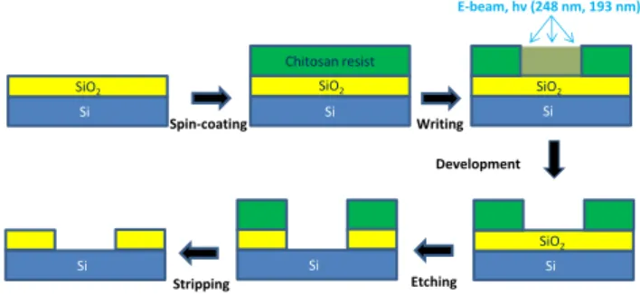
Herein, we proposed to replace current resists by another biopolymer, which is chitosan, for lithography and etching process as displayed in Figure 1.
Figure 1 : Lithography and etching process applied on the chitosan bioresist film.
Chitosan is a polysaccharide constituted of D-glucosamine and D-glucosamine units. The number of N-acetyl-D-glucosamine units along a chain corresponds to the degree of acetylation (DA, in percentage). Chitosan is prepared from chitin, the N-acetyl-D-glucosamine polysaccharide13 (DA = 100 %). This polymer is the second most abundant on Earth after cellulose. It is present in the exoskeleton of arthropods and industrially extracted from the waste from sea food industry as crabs and shrimps shells. Chitosan is also a biodegradable, biocompatible and non-toxic polymer. Due to these properties, it was already used in biotechnology as an adhesion film for the cell culture 14–16. Recent works used chitosan as positive tone resist for e-beam lithography17,18. Patterns of holes of 500 nm spaced by 1.5 µm with development in water have been realized but no transfer of these patterns into the underlying substrate was reported. We demonstrated that unmodified chitosan could be used as a positive tone resist in a complete lithography/ etching process, using 30 kV e-beam lithography. 50 nm patterns were obtained and transferred by plasma etching into silica layer using a completely free organic solvent process19. The chitosan film resistance to etching by CHF3 plasma was assessed
through its selectivity corresponding to the ratio between etching rate of silica on etching rate of chitosan. The selectivity was more than 4.25 and appeared slightly higher than the resistance of PMMA (950-PMMA-A4 from Microchem) which is a common resist in lithography19.
Etching Development Spin-coating Writing Si SiO2 Si Chitosan resist Si SiO2 E-beam, hν (248 nm, 193 nm) Si SiO2 Si Si Stripping SiO2
3
In this work, we aim to demonstrate that the unmodified chitosan can be a universal green resist for lithography (e-beam and UV) allowing sub-micron resolution with possibility of transfer into a silica layer.
2. EXPERIMENTAL
2.1 Materials
Highly deacetylated chitosan was provided by Mahtani Chitosan PVT, Ltd (India) from squid pens and further purified according to the procedure of Rinaudo13. Its molar mass of 570 kg.mol-1 was measured by size exclusion chromatography. Chitosans of DA of 2 % and 35 % were then prepared. DA was quantified by 1H NMR using an AVANCE III 400 MHz spectrometer. Deionized water (ultrapure, 18 MΩ) and acetic acid (Fluka Analytical, glacial acetic acid) were used. Chitosan films were deposited on silica/ silicon substrates using classical spin-on technology. The silica layer (90 nm or 200 nm) was obtained by plasma enhanced chemical vapour deposition. In the case of photolithography at 248 nm, a natural dye, riboflavin (Sigma-Aldrich, 98 %, extracted from Ermothycium ashbyii), was added in the chitosan solution.
2.2 Methods for chitosan film preparation and characterizations
Aqueous diluted acetic acid solution was used to dissolve solid chitosan at concentration of 0.7 % (w/v) or 0.9 % (w/v), depending on the desired thickness. Acetic acid was stoichiometrically added with respect to the free amines of the glucosamine residues. Chitosan films were prepared on silica/silicon substrates by 30 s of spin-coating at 5000 rd.min-1 and 3000 rd.s-2 followed by a softbake at 100 °C for 1 min on a hotplate. It is well known that chitosan through hydrogen bonds have a strong adhesion on silica and silicon surfaces thanks to surface SiOH groups20.
Film thickness was measured by ellipsometry with a spectroscopic ellipsometer UVISEL ™ from Horiba using the classical formula dispersion as model in the Horiba software. The model was adapted to chitosan by adjusting the refractive index between 1.5-1.6 and the extinction coefficient to 0 at 630 nm21.
X-ray reflectivity was performed on an X-ray diffractometer from SmartLab using the Kα1 copper ray to determine the chitosan films density.
For photolithography at 248 nm, riboflavin was added in the chitosan (0.9 % (w/v)) solution at a concentration of 2.2 x 10⁻⁴ mol.L-1, maximum of riboflavin solubility in our conditions. Chitosan-riboflavin films were deposited on silica-silicon substrates following the same protocol as previously described.
In order to determine the distribution of riboflavin in the chitosan films, Two Photon Emission Fluorescence (TPEF) measurements (non-linear optic measurements) were carried out at Institut Lumière Matière. The non-linear optic experimental setup was based on a frequency doubled femtosecond Er-doped fiber laser source (Menlo Lasers, C-Fiber 780). The laser provided pulses with a duration of about 100 fs at a repetition rate of 100 MHz. The fundamental wavelength was set at 780 nm (spectral width of 13 nm) and an average power of about 65 mW was measured at the laser exit. The light beam was focused by a standard microscope objective (magnification X20, NA 0.75) mounted onto a microscope stand (Nikon Eclipse TE2000-U with 3D positioning in inverted geometry) holding the sample. Galvanometric mirrors allowed a beam swept to acquire non-linear images of various samples. The nonlinear optical signals, TPEF, were collected into an optical fiber feeding a spectrometer after going through mirrors and various color filters. These filters were placed on the emission light beam path to avoid any unwanted fundamental. A cooled photomultiplier tube was placed after the spectrometer.
4
2.3 Lithography and developmentE-beam lithography was performed at 100 kV on an e-beam Writer JEOL JBX-9300FS with a ZrO/W thermal field emission source was used at the Plateforme Technologique Amont (PTA) in Grenoble. For 100 kV accelerating voltage, the electron beam has a diameter Gaussian spot of 4 nm, a speed of 50 MHz for a current range of 50 pA -100 nA. Photolithography at 193 nm was performed at the Institut de Science des Matériaux de Mulhouse with a home-made DUV interferometric setup using a 193 nm ArF laser (Braggstar from Coherent) and phase masks generating regular sinusoidal patterns with periods ranging from 100 nm to 600 nm.
Photolithography at 248 nm was performed at PTA on a MBJB4 DUV SUSS Micro Tec device with a density power of 4 mW.cm-2 and a lamp power of 500 W.
Lithography is followed by development in deionized water (18 MΩ) during 60 s.
2.4 Etching process
Etching selectivity study of chitosan films was carried out in a Reactive Ion Etcher (RIE) Corial 200S using CHF3 gas
reactant (usually used for silica etching) during 2 min under 100 sccm of CHF3 at a pressure of 50 mTorr at 20°C for a
power of 140 W (corresponding to a bias voltage of 590 V). Chitosan was, then, selectively removed by O2 plasma for 1
min under 100 sccm of O2 at 100 mTorr, 20 °C, 100 W and bias voltage of 460 V. 2.5 Patterns characterizations
Patterns observations were realized by scanning electron microscopy (SEM) on a scanning electron microscope JEOL JSM 7401F at 2 kV, 5 µA and a working distance of 4 mm. The Image J software was used for the analysis of the SEM images to measure the size of the patterns.
The AFM characterization was carried out with a PicoPlus AFM from Molecular Imaging, in resonant mode.
2.6 UV-visible spectroscopy
The absorbance of the chitosan resist solutions for photolithography was measured by a SAFAS UVmc2 double beam spectrometer with quartz cuvettes of 1 cm. The blank was realized with an aqueous solution of acetic acid (0.05 mol.L-1) in a quartz cuvette.
The absorbance of the chitosan film was measured by a Cary 5G UV-vis-NI spectrophotometer with 2 reflexions at 45°. Data were treated with the Scan software to obtain the film absorbance.
3. RESULTS AND DISCUSSION
3.1 Film properties
In the introduction, the selectivity of chitosan resist to plasma etching was already presented. We previously demonstrated that chitosan films were stable at temperature up to 200 °C and were stable during development in water19. Herein, we will discuss particularly about the absorbance of the film for the photolithographic aspect and their thickness.
5
For photolithography, it is of prime importance that the resist can absorb the energy of the wavelength to generate chemical reactions. The absorbance of a chitosan (DA 2 %) film was measured as displayed in Figure 2.
Figure 2: Chitosan film absorbance (thickness of 180 nm). Substrate absorbance is given as reference.
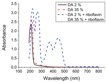
On Figure 2, some interference fringes can be seen but the chitosan film absorbance is very low particularly at 248 nm corresponding to the wavelength of the photomasker we used. The low absorbance at this wavelength is confirmed for chitosan in solution for chitosan of low DA (2 %) but also at high DA (35 %) as displayed in Figure 3. This figure corresponds to the chitosan absorbance spectrum in solution for a concentration of 0.9 % (w/v). On the contrary, it seems that, for photolithography at 193 nm, chitosan absorbance in solution is higher than at 248 nm. Indeed, at 193 nm, absorbance is of 1.6.
Figure 3: UV-visible spectra of a solution of chitosan of DA = 2 and 35 % concentrated at 0.9 % (w/v) in deionized water and acetic acid (0.05 mol.L-1) solutions with and without riboflavin (concentrated at 2.2 x 10⁻⁴ mol.L-1). Blank was made in a quartz cuvette with an aqueous acetic acid solution (0.05 mol.L-1).
In order to improve chitosan absorbance and so chitosan photosensitivity, a natural dye, riboflavin or B2 vitamin, was
added in the formulation of the resists. It is a natural and hydrosoluble dye present in fruits, vegetables and animals22 and extracted from flavinogenic microorganisms23. It is known to generate the photodegradation of organic compounds
200 300 400 500 600 700 800 0.2 0.4 0.6 0.8 1.0 1.2 1.4 1.6 1.8 2.0 2.2 2.4 Fi lm a bs orb an ce Wavelength (nm) Si/SiO2 substrate Chitosan film 100 200 300 400 500 600 700 800 0.0 0.5 1.0 1.5 2.0 2.5 3.0 3.5
Ab
so
rb
a
n
ce
Wavelength (nm)
DA 2 % DA 35 % DA 2 % + riboflavin DA 35 % + riboflavin6
(pesticides, food …) under UV-visible light24. Riboflavin was added at the concentration of 2.2 x 10⁻⁴ mol.L-1 corresponding to its maximum solubility in deionized water in our conditions. At 248 nm, the optical absorption of the chitosan- riboflavin resist solution was significantly increased (Figure 3). Indeed the absorbance of the solution was of 2.5 with riboflavin whatever the chitosan DA and only of 0.25 without riboflavin.
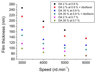
The addition of riboflavin being required for photolithography at 248 nm, we studied the effect of its presence in the film particularly the possibility to make a film and its distribution into this film. Chitosan- riboflavin films were deposited by spin-coating at 3000 rd.s-2 for 30 s followed by a softbake at 100 °C for 1 min. Chitosan of DA 2 % and 35 % were tested for two concentrations. The film thickness as a function of the DA for two concentrations (0.7 % and 0.9 % (w/v)) is displayed in Figure 4. Film thicknesses are shown for chitosan with riboflavin (2.2 x 10⁻⁴ mol.L-1) and without it.
Figure 4 : Spin-curves for chitosan bioresists for two DA (2 % and 35 %) and two concentrations (0.9 % and 0.7 % (w/v)) with or without riboflavin.
Chitosan- riboflavin films could be obtained by spin-coating. The spin-curves on Figure 4 for chitosan – riboflavin films present the same profile and similar thickness than those obtained with chitosan alone. With or without riboflavin, the film thickness depends on the concentration of the polymer as expected but also on the DA. Indeed, spin-coated film thickness depends on inverse of the square of the dynamic viscosity of the polymer solution25. This viscosity relies on the quality of the solvent to dissolve the polymer and to the concentration of polymer. When a polymer is dissolved in a good solvent, its chains are completely spread leading to an increase in the viscosity26. In the case of low DA chitosan in an acidic solution, the chains were totally protonated. They could spread easily. At higher DA, less amino groups were protonated. Even though N-acetyl group is polar, the solvent quality, under similar conditions, decreased reducing the chitosan solubility as observed by Rinaudo et al.27, Anthonsen et al.28 and Wang et al.29. Chains were less spread and the viscosity was consequently lowered. Therefore, viscosity and the film thickness decreased from low DA to high DA as we noticed. The increase in thickness with concentration could be explained, according to Rinaudo et al.27, by the fact that, at these concentrations and in these conditions, chitosan could be assumed in a semi-diluted concentration. Chitosan chains would then be very close ones to others generating entanglements which would limit the flow. The higher the concentration, the higher the number of entanglements, hence the increase in viscosity and in film thickness.
In order to determine if riboflavin was homogeneously distributed in a chitosan film, chitosan –riboflavin films deposited by spin-coating on the silica- silicon substrate were analysed by a non-linear optic measurement Two Photon Excited
3000 4000 5000 6000 60 80 100 120 140 160 180 200 220 240 260 DA 2 % at 0.9 % DA 2 % at 0.9 % + riboflavin DA 35 % at 0.9 % DA 35 % at 0.9 % + riboflavin DA 2 % at 0.7 % DA 35 % at 0.7 % F ilm th ickn e ss ( n m ) Speed (rd.min-1)
7
Fluorescence (TPEF). For a maximal efficiency of riboflavin, it was of prime importance that riboflavin repartition was well distributed in the film. The TPEF measurements gave us access to a three-dimensional resolution. Indeed, the material was excited by two synchronous photons, thus the non-linear optical process only occurred at the focus of the beam. Firstly, TPEF spectra for a chitosan film and a riboflavin-chitosan film with a 780 nm wavelength excitation were recorded (Figure 5).
Figure 5 : TPEF spectra for a pure chitosan film and a mixed riboflavin-chitosan film with a 780 nm wavelength excitation.
In both cases, a peak of the half of the 780 nm excitation wavelength is observed on Figure 5 corresponding to a second harmonic response of these two films due to chitosan. We noticed that chitosan alone was not fluorescent. On the contrary chitosan-riboflavin film presented a high TPEF intensity centred at 512 nm. Thus this fluorescence was only due to riboflavin.
TPEF signal integrated over the 410 - 650 nm spectral region as a function of the film depth was then recorded (Figure 6).
Figure 6 : TPEF signal integrated over the 410 - 650 nm spectral region as a function of the film depth for chitosan + riboflavin film and the reference (SiO2 layer on Si substrate).
According to the previous TPEF spectra, the TPEF signal was only due to riboflavin. On the Figure 6, a TPEF peak appears in the region focused on the chitosan –riboflavin layer (thickness of 150 nm). The reference corresponding to the SiO2 layer on silicon substrate was obtained in absence of chitosan and riboflavin and was shifted due to a different
position of the sample. This depth profile measurement resulted from the convolution of the beam focus and the film
300 400 500 600 700 0 20 40 60 80 100 120 140 160 T PE F In te n sity ( a rb . u n it.) Wavelength (nm) Chitosan+riboflavin Chitosan -25 -20 -15 -10 -5 0 5 10 15 20 25 0 500 T PE F in te n sity ( a rb . u n it.) Depth (µm)
Si- SiO2 substrate Chitosan + riboflavin
8
depth. Hence a TPEF maximum indicated that at the resolution imposed by the beam waist (few micrometers), riboflavin was distributed rather homogeneously within the film.
According to these studies, riboflavin enhanced the chitosan photosensitivity for photolithography at 248 nm and is homogeneously distributed in the chitosan film.
The following parts of this work will now focused on the results obtained in lithography (e-beam, 248 nm and 193 nm) and in transfer with this bioresist.
3.2 Electron beam lithography
Firstly, Monte- Carlo simulations were undertaken to simulate the behaviour of electrons through a chitosan film deposited on a silicon substrate with a silica layer of 90 nm. The results were then compared to the ones for a PMMA film (70 nm in the experimental conditions for 950-PMMA-A4 from Microchem). Results are displayed in the Figure 7. Simulations were realized on the CASINO software for an electron beam with a diameter of 10 nm for 200 electrons accelerated at 100 kV. Density of the different material was 0.88 for chitosan for DA 2 % measured by X-ray reflectometry and already registered in the database 1.74 for silica, 2.33 for siliconand 1.18 for PMMA densities.
Figure 7 : Monte- Carlo simulations of the trajectory of 200 electrons at 100 kV for a sample of resist (a) chitosan or (b) PMMA on silica and silicon. Primary electrons are in blue, backscattered electrons are in red.
Profile obtained for PMMA is similar to the one obtained for a 500 nm layer of PMMA by Urbánek et al.30 with the
CASINO software. In both case, the electron beam passes through the polymer layer without any scattering. Back scattering took place randomly from the silicon substrate for around 10 % of electrons. These simulations suggested that chitosan could behave as PMMA under an electron beam and validated the use of chitosan as resist for e-beam lithography. PMMA 70 nm Silica 90 nm Silicon Chitosan 90 nm Silica 90 nm Silicon 12600 nm 60412 nm 10800 nm 54521 nm (a) (b)
9
For electron beam lithography, we used chitosan of DA of 2 % concentrated at 0.7 % (w/v) on silicon substrate with a silica layer of 90 nm. The film thickness in these conditions was of 80 – 90 nm. Development was performed in deionized water during 60 s.
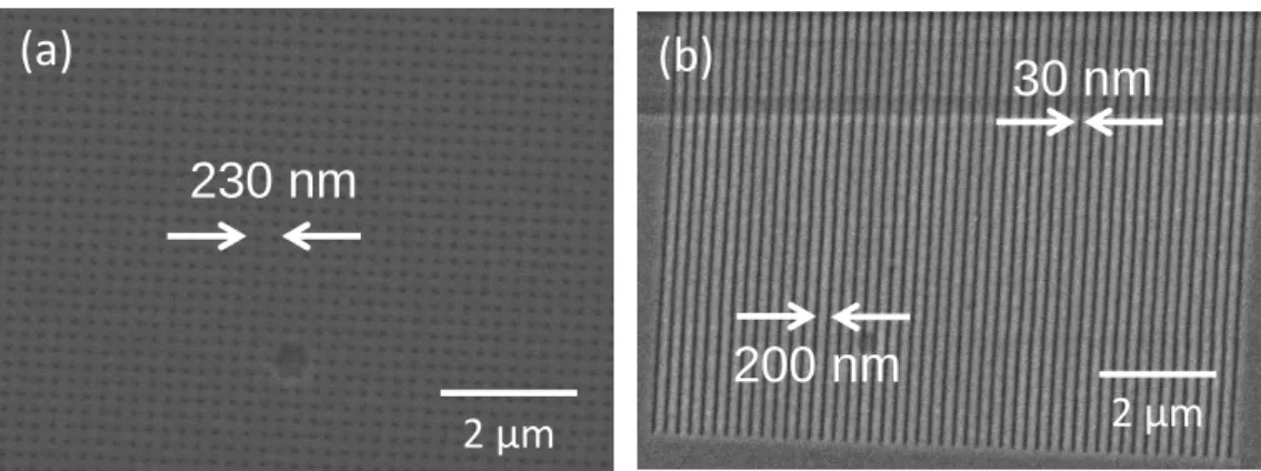
At previous studies with our 30 kV e-beam writer, we demonstrated that high resolution patterns were obtained in a chitosan film with 50 nm lines spaced by 300 nm or 500 nm19. Line edge roughness was low in both cases, respectively of 19 nm and 14 nm. In comparison, Voznesenskiy et al.17,18 who also worked on chitosan films in e-beam lithography (25 kV, deionized water as developer) obtained 500 nm holes spaced by 1.5 µm. At this point, we went further by increasing the resolution and demonstrating the high quality of the final patterns. Such resolution is similar at the one obtained by Takei et al.6 but for a lower electron energy than in their case (75 kV) and for an unmodified biopolymer. In order to validate chitosan as e-beam resists, next studies were performed with a 100 kV standard e-beam writer. Submicronic 2 D holes (Figure 8 a) and 1 D lines (Figure 8 b) patterns were patterned at 200 µC.cm-2 at 100 kV. Figure 8 a and b show the preliminary results after development in deionized water. Holes and lines of 30 nm spaced by 200 nm were obtained. There are well consistent to the results obtained by Kim et al.10 who have patterned 30 nm holes spaced by 100 nm with an e-beam writer at 125 kV. Next work will focus on the optimization of exposure dose.
Figure 8 : SEM images of patterns obtained in a chitosan bioresist by e-beam lithography (100kV, 200 µC.cm-2) and development in deionized water (1 min) (a) 30 nm holes spaced by 200 nm and (b) 30 nm lines spaced by 200 nm.
3.3 Photolithography at 248 nm
UV light at 248 nm irradiation of chitosan was reported to generate the chitosan degradation by a free radical photo-oxidation mechanism31,32. But degradation could occur only for high doses of exposure (2 h to 8 h at 248 nm with a dose density of 0.263 J.cm-2.min-1) as presented by Sionkowska et al.33. Indeed, as demonstrated in section 3.1 film properties, the adsorption of chitosan (DA 35 %, film thickness 90 nm prepared from a solution concentrated at 0.9 % (w/v)) at 248 nm is low. We assessed that 50 minutes exposure (11988 mJ.cm-2) was not sufficient to develop the patterns throughout the chitosan layer: only 10 nm thickness of the exposed area could be dissolved. Given these results and the low absorbance of the film, the addition of a photoactive agent, riboflavin, in the chitosan resist appears of interest. For the two chitosans with riboflavin (films prepared from a solution concentrated at 0.9 % (w/v) in chitosan and 2.2 x 10⁻⁴ mol.L-1 in riboflavin), patterns were obtained with high quality. For DA 2 %, a dose of 10800 mJ.cm-2 enabled to reveal patterns but only on the top surface (10 nm) of the chitosan film. On the contrary, using a DA 35 %, for the same dose of 10800 mJ.cm-2, the patterns were reproduced into the whole thickness of chitosan film (Figure 9) with high fidelity to the mask.
2 µm
230 nm
(a)
2 µm
200 nm
30 nm
(b)
10
Figure 9 : (a) Optical and (b) SEM images of the patterns after lithography at 248 nm (10800 mJ.cm-2) and development in deionized water for 1 min. Patterns of the mask are non-exposed squares of 440 µm x 440 µm spaced of 60 µm exposed lines.
DA appeared to have a significant effect on the photosensitivity at 248 nm. At DA 2 % or 35 %, patterns were revealed but at 35 %, riboflavin efficiency was dramatically increased. In both cases, photodegradation took place partly due to the exposure at the 248 nm as demonstrated by Sionkowska et al.33 and Wasikiewicz et al.32. At this effect, we can add the photodegradation caused by riboflavin. Under UV light, riboflavin is known to be excited which allowed the formation of reactive oxygen species (ROS) as O2 in excited singlet or triplet state, O2•- or H2O224,34. These ROS can
react with chitosan by radical reactions to break the glycosidic bond. Given that the apparent increase of photoefficiency for DA 35 %, an additional possible mechanism can also occur since for a polymer with C=O group in presence of another molecule or polymer with C=O group, a vibrational mixing between these C=O groups can be observed35. When the molecule was excited, an energy transfer could take place through this mixing leading to the excitation of the first polymer and, eventually, to its photodegradation. As chitosan at DA 35 % has more C=O groups than at DA 2 % and as riboflavin also has C=O groups, such mechanism could occur and explain this improvement of efficiency with DA 35 %. On these bases, the study was pursued by increasing the resolution using mask with patterns of less than 0.3 µm. Results are displayed on the Figure 10after development.
Figure 10 : Optical image of 0.3 µm patterns obtained in a chitosan DA 35 % - riboflavin film by photolithography at 248 nm (6400 mJ.cm-2) and revealed by development in deionized water during 1 min.
As for e-beam lithography, it was possible to write sub-micronic patterns into a chitosan-riboflavin film. These preliminary results are very encouraging. However, the photosensitivity should be improved in order to reduce the exposure time. 3.4 Photolithography at 193 nm 500 µm 100 µm
(b)
(a)
1.5 µm11
In photolithography at 193 nm, the two chitosans (low DA at 2 % and high DA at 35 %) were tested. The same chitosan films than for e-beam lithography (chitosan concentrated at 0.7 % (w/v)) were tested with DUV doses ranging from 100 mJ to 2000 mJ. Irradiation was followed by a development in deionized water during 60 s. For DA of 35 %, no patterns could be obtained in the bioresist whatever the applied dose. On the contrary, low DA chitosan films appeared of interest as we can see on the Figure 11.
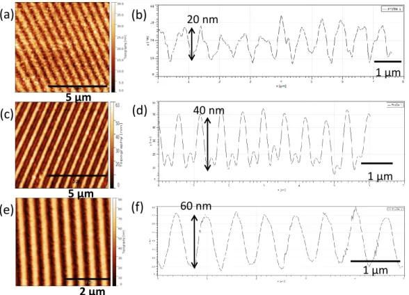
Figure 11 : AFM images and profiles of patterns obtained in a chitosan bioresist film after photolithography at 193 nm and development in deionized water for 1 min for (a, b) 300 mJ, (c,d) 500 mJ and (e, f) 1000 mJ.
On Figure 11
,
patterns appeared for doses superior to 300 mJ (Figure 11 a and b). The dose was however too low to reveal patterns on the total thickness of the film. By increasing it steadily, reproduction of patterns was of better quality and their depth was steadily increased as we can observe on the Figure 11 (c to f). At 1000 mJ (Figure 11 e and f) SiO2layer was almost reached, the film thickness of chitosan was of 90 nm. Profile of the patterns was sinusoidal suggesting that the chitosan resist has a linear response under deep UV exposure instead of a binary one. Interestingly, the dose needed to pattern the chitosan bioresist is in the same order of magnitude to standard photoresists used in the same setup. These first results need to be optimized and the photochemical pathway is still under investigation but they are promising for the use of chitosan bioresist for 193 nm.
3.5 Transfer by etching
In several applications and particularly in microelectronics, lithography is followed by a step of transfer. We studied the transfer by reactive ion etching by CHF3 plasma.
(a)
2 µm
(d)
(c)
(f)
(e)
5 µm
5 µm
1 µm
20 nm
1 µm
40 nm
1 µm
60 nm
(b)
12
Transfer into silica by CHF3 plasma etching during 4 min and stripping by O2 plasma for 2 min were applied on chitosan
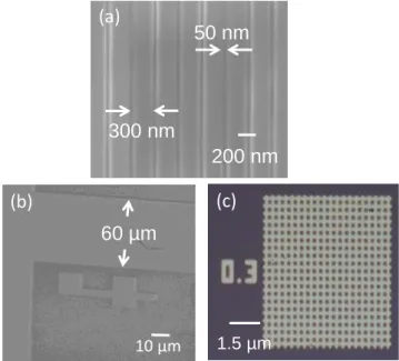
and chitosan - riboflavin films after lithography. Previously, we assessed the chitosan selectivity at 4.2519. In the Figure 12, examples of patterns after transfer and stripping after photolithography are also displayed.
Figure 12 : SEM images of patterns after transfer by reactive ion etching of CHF3 plasma and stripping by O2 plasma obtained (a) by
e-beam lithography (30 kV) 50 nm lines spaced by 300 nm from Caillau et al.19 and by photolithography at 248 nm (10800 mJ.cm-2) (b) 60 µm lines and (c) optical image of 0.3 µm patterns (6400 mJ.cm-2).
In Figure 12 a, were displayed the patterns obtained by 30 kV e-beam lithography after transfer and stripping from a chitosan DA 2 % film. We noticed that even for high resoluted patterns obtained by e-beam lithography was of high quality with very low line edge roughness of only 5 nm19. In photolithography, the transfer was also successfully done for chitosan DA 35 %- riboflavin films as shown in the Figure 12 b for photolithography at 248 nm. The size was still well respected with squares of (436 ± 5) µm and width of the lines of (60 ± 1) µm. Figure 12 c displays that such quality of transfer was also reached for sub-micronic resoluted mask patterns in photolithography.
It was demonstrated that addition of riboflavin to chitosan did not impair the selectivity of the chitosan allowing for the transfer of the patterns by CHF3 plasma. Therefore, these experimental results open the possibility of using chitosan as a
resist for e-beam lithography and photolithography followed by fluorinated gas plasma etching.
4. CONCLUSIONS
Aiming at developing green resist for lithography, a biopolymer, chitosan, issued from waste repurposing was proposed for a complete lithography and etching process. In addition, no chemical modification of chitosan nor any oil-based and toxic chemical were necessary.
Only water was used as a solvent. We also demonstrated that chitosan is a ubiquitous positive tone resist allowing for e-beam lithography at 30 kV and 100 kV as well as photolithography at 193 and 248 nm. In the latter case, a natural, water soluble, non-toxic photoactivator was needed: riboflavin. We showed that the DA affect the effectiveness of the riboflavin promoted reaction.
200 nm
300 nm
50 nm
10 µm
(b)
60 µm
(a)
1.5 µm(c)
13
Next works will focus on the increase of sensitivity for UV lithography particularly at 248 nm.
ACKNOWLEDGEMENTS
Nanolyon platform is acknowledged for equipment and support. Thierry Chevolleau and Christophe Lemonias from the Plateforme Technologique Amont of Grenoble are acknowledged for access, equipment and technical support. Green lithography project is supported by Pulsalys. EEA doctoral school is acknowledged for the doctoral scholarship for Mathieu Caillau.
REFERENCES
[1] Clark, J. H., “Green chemistry : challenges and opportunities,” Green Chem. 1(1), 1–8 (1999).
[2] Anastas, P. T. and Kirchhoff, M. M., “Origins , Current Status , and Future Challenges of Green,” Acc. Chem. Res. 35(9), 686–694 (2002).
[3] Karn, B., “The road to green nanotechnology,” J. Ind. Ecol. 12(3), 263–266 (2008). [4] Smith, G. B., “Green nanotechnology,” Proc. SPIE 810402 (2011).
[5] Levinson, H. J., “Lithography - Green and getting greener,” Jpn. J. Appl. Phys. 50(6 part 2), 06GA01 (2011). [6] Takei, S., Oshima, A., Sekiguchi, A., Yanamori, N., Kashiwakura, M., Kozawa, T. and Tagawa, S., “Electron beam
lithography using highly sensitive negative type of plant-based resist material derived from biomass on hardmask layer,” Appl. Phys. Express 4(10), 106502 (2011).
[7] Takei, S., Oshima, A., Wakabayashi, T., Kozawa, T. and Tagawa, S., “Eco-friendly electron beam lithography using water-developable resist material derived from biomass,” Appl. Phys. Lett. 101(3), 33106 (2012).
[8] Takei, S., Oshima, A., Ichikawa, T., Sekiguchi, A., Kashiwakura, M., Kozawa, T., Tagawa, S., Oyama, T. G., Ito, S. and Miyasaka, H., “Organic solvent-free water-developable sugar resist material derived from biomass in green lithography,” Microelectron. Eng. 122, 70–76 (2014).
[9] Takei, S., Oshima, A., Oyama, T. G., Ito, K., Sugahara, K., Kashiwakura, M., Kozawa, T., Tagawa, S. and Hanabata, M., “Application of natural linear polysaccharide to green resist polymers for electron beam and extreme-ultraviolet lithography,” Jpn. J. Appl. Phys. 53(11) (2014).
[10] Kim, S., Marelli, B., Brenckle, M. A., Mitropoulos, A. N., Gil, E.-S., Tsioris, K., Tao, H., Kaplan, D. L. and Omenetto, F. G., “All-water-based electron-beam lithography using silk as a resist.,” Nat. Nanotechnol. 9(4), 306–310 (2014).
[11] Park, J., Lee, S.-G., Marelli, B., Lee, M., Kim, T., Oh, H.-K., Jeon, H., Omenetto, F. G. and Kim, S., “Eco-friendly photolithography using water-developable pure silk fibroin,” RSC Adv. 6(45), 39330–39334 (2016).
[12] Jiang, B., Yang, J., Li, C., Zhang, L., Zhang, X. and Yang, P., “Water-Based Photo- and Electron-Beam Lithography Using Egg White as a Resist,” Adv. Mater. Interfaces 4(7), 1601223 (2017).
[13] Rinaudo, M., “Chitin and chitosan: Properties and applications,” Prog. Polym. Sci. 31(7), 603–632 (2006).
[14] Park, I., Cheng, J., Pisano, A. P., Lee, E. S. and Jeong, J. H., “Low temperature, low pressure nanoimprinting of chitosan as a biomaterial for bionanotechnology applications,” Appl. Phys. Lett. 90(2007), 32–35 (2007).
[15] Fernandez, J. G., Mills, C. A., Martinez, E., Lopez-Bosque, M. J., Sisquella, X., Errachid, A. and Samitier, J., “Micro- and nanostructuring of freestanding, biodegradable, thin sheets of chitosan via soft lithography,” J. Biomed. Mater. Res. - Part A
85(1), 242–247 (2008).
[16] Cheng, J. C., Cauley, T. H. and Pisano, A. P., “Lithographic patterning of immobilized enzymes in chitosan thin films for multi-layer, chemical/biological sensors,” Proc. 7th IEEE, 334–337 (2007).
[17] Voznesenskiy, S., Nepomnyaschiy, A. and Kulchin, Y., “Study of Biopolymer Chitosan as Resist for Submicron Electronic Lithography,” Solid State Phenom. 213, 180–185 (2014).
[18] Voznesenskiy, S. and Nepomnyaschiy, A., “Dose Characteristics of Multilayer Chitosan-Metal-Dielectric Nanostructures for Electronic Nanolithography,” Solid State Phenom. 245, 195–199 (2015).
[19] Caillau, M., Laurenceau, E., Chevolot, Y., Leclercq, J., Alekseev, S., Chevalier, C. and Delair, T., “Fifty nanometer lines patterned into silica using water developable chitosan bioresist and electron beam lithography,” J. Vac. Sci. Technol. B, Nanotechnol. Microelectron. Mater. Process. Meas. Phenom. 35(6), 06GE01 (2017).
[20] Laskowski, J. S., Liu, Q. and O’Connor, C. T., “Current understanding of the mechanism of polysaccharide adsorption at the mineral/aqueous solution interface,” Int. J. Miner. Process. 84(1–4), 59–68 (2007).
[21] Nosal, W. H., Thompson, D. W., Yan, L., Sarkar, S., Subramanian, A. and Woollam, J. A., “UV-vis-infrared optical and AFM study of spin-cast chitosan films,” Colloids Surfaces B Biointerfaces 43(3–4), 131–137 (2005).
[22] Sheraz, M. A., Kazi, S. H., Ahmed, S., Anwar, Z. and Ahmad, I., “Photo, thermal and chemical degradation of riboflavin,” Beilstein J. Org. Chem. 10, 1999–2012 (2014).
14
[23] Demain, A. L., “Riboflavin oversynthesis,” Annu. Rev. Microbiol. 26, 369–388 (1972).
[24] Escalada, J. P., Pajares, A., Gianotti, J., Biasutti, A., Criado, S., Molina, P., Massad, W., Amat-Guerri, F. and García, N. A., “Photosensitized degradation in water of the phenolic pesticides bromoxynil and dichlorophen in the presence of riboflavin, as a model of their natural photodecomposition in the environment,” J. Hazard. Mater. 186(1), 466–472 (2011).
[25] Emslie, A. G., Bonner, F. T. and Peck, L. G., “Flow of a Viscous Liquid on a Rotating Disk,” J. Appl. Phys. 29(5), 858–862 (1958).
[26] Flory, P. J., “Thermodynamics of High Polymer Solutions,” J. Chem. Phys. 10(1), 51–61 (1942).
[27] Rinaudo, M., Milas, M. and Dung, P. Le., “Characterization of chitosan. Influence of ionic strength and degree of acetylation on chain expansion,” Int. J. Biol. Macromol. 15(5), 281–285 (1993).
[28] Anthonsen, M. W., Vårum, K. M. and Smidsrød, O., “Solution properties of chitosans: conformation and chain stiffness of chitosans with different degrees of N-acetylation,” Carbohydr. Polym. 22(3), 193–201 (1993).
[29] Wang, W. and Xu, D., “Viscosity and flow properties of concentrated solutions of chitosan with different degrees of deacetylation,” Int. J. Biol. Macromol. 16(3), 149–152 (1994).
[30] Urbánek, M., Kolařík, V., Krátký, S., Matějka, M., Horáček, M. and Chlumská, J., “Monte Carlo Simulation of Proximity Effect in E-Beam Lithography,” NANOCON 2013 - Conf. Proceedings, 5th Int. Conf., 723–726 (2013).
[31] Sionkowska, A., Wisniewski, M., Skopinska, J., Vicini, S. and Marsano, E., “The influence of UV irradiation on the mechanical properties of chitosan/poly(vinyl pyrrolidone) blends,” Polym. Degrad. Stab. 88(2), 261–267 (2005).
[32] Wasikiewicz, J. M., Yoshii, F., Nagasawa, N., Wach, R. A. and Mitomo, H., “Degradation of chitosan and sodium alginate by gamma radiation, sonochemical and ultraviolet methods,” Radiat. Phys. Chem. 73(5), 287–295 (2005).
[33] Sionkowska, A., Kaczmarek, H., Wisniewski, M., Skopinska, J., Lazare, S. and Tokarev, V., “The influence of UV irradiation on the surface of chitosan films,” Surf. Sci. 600(18), 3775–3779 (2006).
[34] Pajares, A., Gianotti, J., Stettler, G., Bertolotti, S., Criado, S., Posadaz, A., Amat-guerri, F. and García, N. A., “Modelling the natural photodegradation of water contaminants A kinetic study on the light-induced aerobic interactions between riboflavin and 4-hydroxypyridine,” J. Photochem. Photobiol. A Chem. 139(2–3), 199–204 (2001).
[35] Amerik, Y. and Guillet, J. E., “The Photochemistry of Ketone Polymers. IV. Photolysis of Methyl Vinyl Ketone Copolymers,” Macromolecules 4(4), 375–379 (1971).
[36] Kubota, N. and Eguchi, Y., “Facile Preparation of Water-Soluble N-Acetylated Chitosan and Molecular Weight Dependence of Its Water-Solubility.,” Polym. J. 29(2), 123–127 (1997).
[37] Won-Seok Choi, Kị-Jin Ahn, Dong-Wook-Lee, M.-W. B., “Preparation of chitosan oligomers by irradiation,” Polym. Degrad. Stab. 78(3), 533–538 (2002).