HAL Id: hal-01387983
https://hal.archives-ouvertes.fr/hal-01387983
Submitted on 6 May 2019HAL is a multi-disciplinary open access archive for the deposit and dissemination of sci-entific research documents, whether they are pub-lished or not. The documents may come from teaching and research institutions in France or abroad, or from public or private research centers.
L’archive ouverte pluridisciplinaire HAL, est destinée au dépôt et à la diffusion de documents scientifiques de niveau recherche, publiés ou non, émanant des établissements d’enseignement et de recherche français ou étrangers, des laboratoires publics ou privés.
VLS Grown 4H-SiC Buried P+ Layers for JFET Lateral
Structures
Selsabil Sejil, Farah Laariedh, Mihai Lazar, Davy Carole, Christian Brylinski,
Dominique Planson, Gabriel Ferro, Christophe Raynaud, Hervé Morel
To cite this version:
Selsabil Sejil, Farah Laariedh, Mihai Lazar, Davy Carole, Christian Brylinski, et al.. VLS Grown 4H-SiC Buried P+ Layers for JFET Lateral Structures. Materials Science Forum, Trans Tech Publications Inc., 2015, 821-823, pp.789 - 792. �10.4028/www.scientific.net/MSF.821-823.789�. �hal-01387983�
VLS grown 4H-SiC buried P
+layers for JFET lateral structures
S. Sejil
1,2a, F. Laariedh
1b, M. Lazar
1c, D. Carole
2d, C. Brylinski
2e,
D. Planson
1f, G. Ferro
2g, C. Raynaud
1h, H. Morel
1i1,2) Université de Lyon, CNRS, France
1) Laboratoire AMPERE, INSA Lyon, Ecole Centrale de Lyon, 69621 Villeurbanne 2) Laboratoire des Multi-matériaux et Interfaces, Université Lyon 1, 69622 Villeurbanne a[email protected], b[email protected], c[email protected], d[email protected], e[email protected], f
[email protected], g[email protected], h[email protected], i[email protected]
Keywords: VLS epitaxial growth, JFET, TLM, roughness
Abstract. Lateral JFET transistors have been fabricated with N and P-type channels
tentatively integrated monolithically on the same SiC wafer. Buried P+ SiC layers grown by
Vapor-Liquid-Solid (VLS) selective epitaxy were utilized as source and drain for the P-JFET and as gate for the N-JFET. The ohmicity of the contacts, both on VLS grown P+ and ion
implanted N+ layers, has been confirmed by Transfer Length Method (TLM) measurements.
A premature leakage current is observed on the P/N junction created directly by the P+ VLS
gate layer, probably due to imperfect VLS (P+) / CVD (N+) SiC interface.
Introduction
Device integration is a key step in the development of higher performance, higher reliability, more compact, and cheaper devices for power electronics. Silicon carbide (SiC) offers excellent properties in terms of maximum electrical field, cooling effort and high temperature operation. With SiC devices integration, the size of converters can be drastically reduced, inducing faster switching operation with lower power losses. Several demonstrators of monolithically integrated SiC active devices, such as VJFET and JBS diodes [1] or vertical and lateral BJT [2] have been already produced. However, the high cost and small diameter of semi-insulating SiC substrates so far, and the high resistivity of the p-type layers, are still impeding the development of such a monolithic technology. Previous investigations have revealed that Vapor-Liquid-Solid (VLS) selective epitaxy can be an interesting method to obtain localized highly p-type doped SiC, leading to considerable reduction of the p-type SiC resistivity and of the specific resistance of the ohmic contacts formed on it. Specific resistance values as low as 1.3×10⁻⁶ Ω.cm2 have been demonstrated previously [3].
In the present work, we have investigated the possibility of using such VLS grown P+ SiC
layers as functional layers in lateral SiC JFET’s. Lateral JFET transistors with N-type and P-type channels have been fabricated, integrated monolithically onto the same SiC wafer. The VLS P+ wells were utilized as source and drain contacting layers for the P-channel JFET and
as P+ gate for the N-channel JFET.
Experimental section
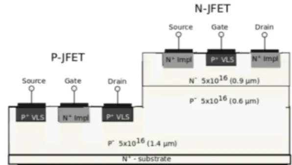
The transistors have been fabricated on commercial 4H-SiC wafers with CVD epitaxial layers grown on N+ substrate. These CVD epilayers have been used for the N and P-type
channels of the JFET. The doping and the thickness of the CVD epitaxial layers are detailed in figure 1.
The different structures are isolated by dry RIE etching using SF6/O2 chemistry and Ni
based hard mask [4]. Compared to the N-JFET structures described in ref [5], a N+ substrate
has been preferred, instead of a semi-insulating one. This conductive substrate can be used as an additional electrode which can be biased at a fixed potential or used as an additional gate for the P-JFET. The N+ wells for the gate of the P-JFET and for the source and drain
electrodes of the N-JFET have been implemented by nitrogen ion implantation and subsequent activation annealing. A “box” profile was created with multiple ion energies over the range 25 - 100 keV with a cumulated dose of 7.4×1014 cm-2. The depth of the junction
induced by N+ wells was thus fixed to about 0.3 µm. The post-implantation annealing has
been performed at 1700°C during 30 min in an RF-heated furnace. Prior to the annealing, the SiC surface has been protected with a C-cap formed by photoresist baking [6].
The P+ wells have been created by VLS buried selective epitaxial growth from Al-Si liquid
phase [7]. The depth of the P+ wells was defined at 0.4µm by preliminary etching of trenches
using the fluorinated RIE process described before. This step is critical because it fixes also the thickness of the N-type channel. After the etching step, Si and Al layers were deposited on the whole wafer in order to fill the trenches. The thickness of each layer was chosen in order to get a total thickness of 1 µm with Al content around 40 at% in the layer stack. The Al/Si layer stack has been patterned by successive wet and dry etching with resist mask, so that the Al-Si liquid phase, formed after melting over 580°C, can fill the trenches and wet onto the trench edges.
The VLS process was then performed by heating the sample, under Ar, up to 1100°C. The propane (1sccm) was added into the gas phase to perform the VLS SiC growth during 5 min. The 1700°C annealing has been performed after this VLS process to improve the quality of the formed P-N junctions, as explained in a previous report [8].
Finally, ohmic contacts have been realized using Ni for the back-side of the N+ substrate
and on N+ wells, and using a specific Ni-Ti-Al alloy on the P+ wells [9]. Both contacts have
been annealed together by Rapid-Thermal-Annealing under Ar at 900°C and 800°C respectively.
For the lateral P-JFET’s and N-JFET’s, two different lay-out variants are present on the masks, namely: inter-digitated fingers and serpentine shapes, with different sizes. Process Control and Monitoring (PCM) patterns were added on the masks including TLM structures, in order to test the ohmic contacts and the resistivity of the different doped layers (N+, P+ and
channel layers). Figure 2 presents an image of a SiC sample with different structures: JFET, TLM and other PCM paterns.
Electrical characterization
All current-voltage (I-V) measurements on JFET’s and TLM structures have been performed with a “Signatone S1160” probe station and a “Keithley 2410” Source Measure Unit (SMU).
Fig. 1. Cross-sectional structure of the integrated P and N lateral JFET
Fig. 2. Optical micrograph recorded after the technological fabrication process
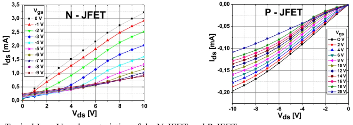
Typical IDS-VDS characteristics, plotted as a function of VGS, are presented in Figure 3 for
both N-JFET’s and P-JFET’s. As expected, the resistivity of the P-channel is higher, as compared to the N-channel, due to the lower mobility of the carriers. For both types of channels, we obtain a modulation of the channel resistivity by varying the VGS gate-source
bias. Note that the VGS range is positive for the P-JFET and negative for the N-JFET. Trying
to reach the pinch-off state on the N-JFET (figure 3), we observed a shift of IDS-VDS
characteristics from the origin of the plot. This seems to be due to a combination between gate leakage and substrate leakage currents.
Fig. 3. Typical IDS - VDS characteristics of the N-JFET and P-JFET
IGS-VGS gate diode characteristics are presented in Figure 4 for a large number of N-JFET
and P-JFET.
Fig. 4. IGS - VGS gate diode characteristics typical of a consistent number of N-JFET and P JFET For both cases case, the typical I-V characteristic of a 4H-SiC bipolar diode should be obtained with a direct threshold voltage around 2.5 V. Experimentally, the expected behavior is only obtained for the P-JFET, which has N+ ion-implanted gate on CVD P-type channel
layer. For the N-JFET, which has P+ VLS gate on CVD N-type channel layer, the gate diode
behaves more like a Schottky diode with low barrier height and rather high reverse leakage current. This anomalous gate diode behavior is probably the cause of the leakage currents observed in the case of N-JFET and a consequence of imperfect VLS (P-type) / CVD (N-type) interface. Studies are in progress to solve this problem.
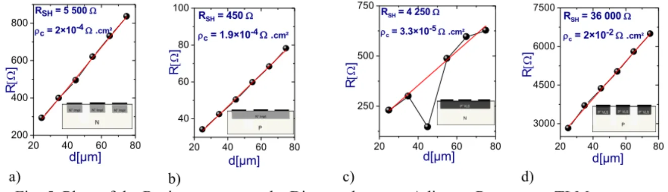
I-V measurements have been performed on TLM test structures on the four types of layers (P+ VLS layer, N+ implanted layer, and N and P epilayers). The results are summarized on
Figure 5. Linear current-voltage characteristics are obtained for the all TLM geometries. Due to the very high doping levels obtained, the contacts have an ohmic behavior on both P+ VLS and N+ implanted layers.
0 2 4 6 8 10 0,0 0,5 1,0 1,5 2,0 2,5 3,0 3,5 N - JFET Vgs 0 V -1 V -2 V -3 V -4 V -5 V -6 V -7 V -8 V -9 V I ds [mA] Vds [V] -10 -8 -6 -4 -2 0 -0,20 -0,15 -0,10 -0,05 0,00 P - JFET Vds [V] Ids [mA ] Vgs O V 2 V 4 V 6 V 8 V 10 V 12 V 14 V 16 V 18 V 20 V -4 -2 0 2 4 -2 0 2 4 6 8 10 12 14 P/N junction: P+(VLS)/N- (CVD) N - JFET Igs [mA] Vgs [V] -4 -2 0 2 4 -16 -14 -12 -10 -8 -6 -4 -2 0 2 P/N junction: P-(CVD)/N+(ion implant.) P - JFET Vgs [V] I gs [mA]
a) b) c) d)
Fig. 5. Plots of the Resistance versus the Distance between Adjacent Patterns on TLM arrays N+ / N (a), N+ / P (b), P+ / N (c) and P+ / P (d).
Optical microscopic observations show a strong surface roughness of the P+ VLS layers
that could explain the difficulty to obtain reproducible resistance values between two TLM patterns (fig. 5c). This phenomenon is not observed on the P+ VLS/P structure (fig.5d) where
the high resistance value mainly corresponds to that of the P-type channel layer.
Conclusion
In this work, lateral J-FET transistors with N and P-type channels were tentatively integrated monolithically on the same SiC wafer. VLS grown P+ wells were utilized as source
and drain electrodes for the P-JFET and as gate for the N-JFET. A premature leakage current and a shift of IDS-VDS characteristics from the origin is observed in the case of N-type JFET. It
could be explained by the imperfect VLS / CVD interface between the VLS grown P+ gate
and N-type channel, which must be improved. Nevertheless, the present work revealed that the P+ VLS layers could already be used to improve the access resistance in SiC devices. Not
only unipolar devices such as our P-JFET could be considered, but also bipolar high voltage devices where the P/N junction is created by CVD epitaxial layers and the VLS P+ layer is
inserted between the P-CVD epilayer and metal contact layer.
Acknowledgments
The authors gratefully thank NanoLyon Technological Platform team for technological means and for training our staff.
References
[1] R. Radhakrishnan and J.H. Zhao, IEEE Electron Device Letters, 32 n° 6 785 (2011).
[2] L. Lanni,B.G. Malm, M. Östling, C-M. Zetterling, IEEE Electron Device Let 35 n°4 428 (2014) [3] N. Thierry-Jebali, M. Lazar, A. Vo-Ha, D. Carole, V. Soulière, A. Henry, D. Planson, G. Ferro, L.
Konczewicz, S. Contreras, C. Brylinski, P. Brosselard Mater. Sci. Forum. 778-780 639 (2014). [4] M. Lazar, M. Lazar, F. Enoch, F. Laariedh, D. Planson, P. Brosselard, Mater. Sci. Forum.
679-680 477 (2011)
[5] K. Fujikawa, T. Masuda, H. Tamaso, K. Shibata, S. Harada, S. Hatsukawa, H. Tokuda, A. Saegusa, Y. Namikawa, SEI TECHNICAL REVIEW 61 77·(2006)
[6] E. Oliviero, M. Lazar, A. Gardon, C. Peaucelle, A. Perrat, J. J. Grob, C. Raynaud, D. Planson, Nucl. Instrum. Meth. B 257 265 (2007)
[7] D. Carole, S. Berckmans, A. Vo-Ha, M. Lazar, D. Tournier, P. Brosselard, V. Soulière, L. Auvray, G. Ferro, C. Brylinski, Mater. Sci. Forum. 717-720 169 (2012)
[8]. N.Thierry-Jebali, M.Lazar, A.Vo-Ha, D. Carole, V. Soulière, F. Laariedh, J. Hassan, A. Henry, E. Janzén, D. Planson, G. Ferro, C. Brylinski, P. Brosselard Mater. Sci. Forum 740-742 911 (2013) [9]. F Laariedh, M Lazar, P Cremillieu, J Penuelas, J-L Leclercq, D Planson, Semicond.Sci Tech 28
045007 (2013) 20 40 60 80 200 400 600 800 RSH = 5 500 W rc = 2×10⁻⁴ W .cm² R [W ] d[µm] 20 40 60 80 40 60 80 100 R [W ] d[µm] RSH = 450 W rc = 1.9×10⁻⁴W .cm² 20 40 60 80 250 500 750 R SH = 4 250 W rc = 3.3×10⁻⁵ W .cm² R [W ] d[µm] 20 40 60 80 3000 4500 6000 7500 RSH = 36 000 W rc = 2×10⁻² W .cm² R [W ] d[µm]