HAL Id: hal-00707741
https://hal.archives-ouvertes.fr/hal-00707741
Submitted on 13 Jun 2012
HAL is a multi-disciplinary open access
archive for the deposit and dissemination of
sci-entific research documents, whether they are
pub-lished or not. The documents may come from
teaching and research institutions in France or
abroad, or from public or private research centers.
L’archive ouverte pluridisciplinaire HAL, est
destinée au dépôt et à la diffusion de documents
scientifiques de niveau recherche, publiés ou non,
émanant des établissements d’enseignement et de
recherche français ou étrangers, des laboratoires
publics ou privés.
3-Dimensional, Solder-Free Interconnect Technology for
high-Performance Power Modules
Bassem Mouawad, Cyril Buttay, Maher Soueidan, Hervé Morel, Bruno Allard,
D. Fabregue, Vincent Bley
To cite this version:
Bassem Mouawad, Cyril Buttay, Maher Soueidan, Hervé Morel, Bruno Allard, et al.. 3-Dimensional,
Solder-Free Interconnect Technology for high-Performance Power Modules. 7th CIPS, Mar 2012,
Nuremberg, Germany. pp.433-438. �hal-00707741�
3-Dimensional, Solder-Free Interconnect Technology for
High-Performance Power Modules
Bassem Mouawad, Cyril Buttay, Maher Soueidan, Hervé Morel and Bruno Allard, Université de
Lyon, INSA de Lyon, AMPERE-UMR 5005, Bât. L. de Vinci, 21 Av. J. Capelle, 69621
Villeurbanne Cedex – France
Damien Fabrègue, Université Lyon, INSA de Lyon, MATEIS-UMR 5510, Bât. B. PASCAL, 7 Av. J.
Capelle, 69621 Villeurbanne Cedex, France.
Vincent Bley, Université de Toulouse, UPS, INPT, LAPLACE 118, route de Narbonne, 31062
Toulouse, France.
Abstract
The classical wire bonding has several drawbacks that make 3D structures a desirable technology for a high performance power module. An interconnection solution for the power semiconductor dies is presented here: it is based on copper micro-posts that are electroplated on top of the die. The die with its micro-posts is then assembled between two Direct Bonding Copper (DBC) substrates using a direct copper-to-copper bond method. This direct bond method is achieved using a Spark Plasma Sintering (SPS) process machine. Manufacturing and electrical characterization of a power semiconductor die with the micro-posts interconnection is presented in details.
1
Introduction
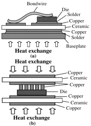
Power semiconductors devices have largely improved since they were first introduced more than 50 years ago. The have now reached a high level of performance, and most of the limitations (in power density, operations temperature or switching speed) come from their environment (i.e. their packaging). Classically, the current manufactured power modules provide a planar package as described in figure 1 (a). It consists in assembling several power dies into a package that provides an electrical insulation (using the ceramic substrate), the thermal management (the heat dissipated by the devices is removed through the ceramic layer) and electrical interconnects where the most common die-level interconnection is wire bonding. Maturity, flexibility and low cost are main factors which explain the use of the wire bonding technology plus recent improvement with respect to lead-free solder regulation or high temperature capability. However, this planar package has become the limiting factor of the performances of the semiconductor modules. A wire bond usually generates a parasitic inductance of about 10 nH [1]. This result in over-voltages at the switch level and constitutes a limiting factor regarding the maximum switching frequency. From a thermal point of view, the heat flux dissipation is limited to one direction (the backside of the dies). This leads to a non-optimal cooling, creating issues such as wire bond fatigue and, eventually, failure [2]. A cooling system that could remove the heat through both sides of the die would be much more efficient.
Figure 1 A planar module (a) and the proposed 3D structure based on micro-posts offering double-side cooling (b)
Alternative interconnection technologies have been developed to overcome the shortcomings of the wire bonding technology. They are based on a
three-dimensional (3D) packaging of power modules in a compact stacked layer structure [3], [4], [5]. The proposed technologies can be divided into four categories: solder interconnection, interconnection by springs, pressure contact and interconnection by electroplated metallization. The advanced interconnection technologies permit a decrease in the values of parasitic inductance and electrical resistance. They also offer opportunities to improve the thermal management, as cooling can be provided to both side of the dies. Our work is based on the interconnection by electroplated metallizations. This paper details a new technology allowing the 3D packaging of power modules called Micro-Posts Interconnection (MPI), which is based on a die with micro-posts bonded directly between two DBC (Figure 1
(b)) [6]. The direct copper-to-copper bonding method is
described in Section 2. Section 3 describes the 3D structure. Results and discussion are given in Section 4. Finally, a conclusion is given in section 5.
2
Direct copper-to-copper bonding
This MPI technique requires, firstly, the electrochemical growth of a copper posts matrix, and secondly the bonding of this die between two DBC by using a Spark Plasma Sintering (SPS) process (described later).The main challenge was to find the proper parameters to achieve a good direct copper-to-copper bond. So we chose to work with a pure bulk copper rod to facilitate the study of the direct copper bond.
2.1 SPS process
The direct copper-to-copper bonds were carried out on a SPS system (FCT HPD 25) at Mateis Laboratory. As with a classical sintering press, a SPS system applies both pressure and heat to the samples. The difference is that the heat is provided by a pulsed DC-current circulating through the graphite die (or through the sample if it is conductive). As a result in the case of the SPS, the heat is generated much closer to the sample, offering very fast temperature dynamics: more than 100 K/min for the system used in this study, using current pulses of several kA (see Figure 2). The temperature was measured by a thermocouple putted inside a hole in the graphite die.
2.2 Copper bonding
Commercial copper rods (Goodfellow, Cambridge, UK, 99.99+% purity) with a diameter of 19 mm and a length of 400mm were used as the base material in the bonding experiment. These rods were cut into 25 mm-long cylindrical pieces with one flat side manually polished. The polishing procedure starts with 220-grit silicon carbide paper, down to 1 μm diamond paste and 0.05 μm silica. The samples were then cleaned to remove the lubricant. The cleaning process found to be successful consisted of (i) ultrasonic cleaning in acetone to remove the lubricant, (ii) ultrasonic cleaning in trichloroethylene, (iii) ultrasonic cleaning in microelectronic grade ethanol, (iv) immersion in 7% HF for 30s at room temperature for oxide elimination (v) followed by rinsing in DI water and
Figure 2 Schematic representation of a SPS sintering machine
Figure 3 Shape of the samples used for tensile test
t (min) T (°C) P (MPa) σ (MPa) A 5 300 77 181 B 20 300 77 239 C 20 300 16 170 D 5 300 16 132 E 5 200 77 106 F 20 200 77 270 G 20 200 16 261 H 5 200 16 0 I 20 200 16 150 Table 1 Measurement summary for different SPS experiments [7]
blow drying with nitrogen gas.
In each experiment, two pieces of copper were put together in SPS machine with the polished sides against each other. After bonding the samples were machined for the mechanical test (tensile test), as described in Figure 3. The bonding was performed in vacuum (10−2 torr) with
temperatures ranging from 200 °C to 300 °C. The uniaxial force applied during the bonding and maintained during the cooling down to room temperature, was varied from 5 kN to 24 kN (corresponding to 16 and 77 MPa on the sample respectively). Some experiments are summarized in table 1; the bonded samples were submitted to a tensile test, in which the strain experienced by the sample, as
well as the force applied, were recorded up to failure. Table 1 lists the bonding parameters as well as the maximum stress (σ) experienced by the samples during the tensile test.
Copper being ductile, the sample quickly enters plastic deformation during the tensile test. This results in the reduction of the actual section of the sample as it elongates. In this document, a nominal stress value is calculated using the initial surface of the tensile sample. It will thus constitute a lower bound of the true stress experienced on the sample, as plastic deformation and then necking occurs before the actual rupture of the sample (hence reducing the surface of the bond). It should be mentioned that all the samples fractured along the bond line (due to the design of the sample). It should be noted that a plain copper sample was found to break at 365 MPa [7].
Table 1 shows that for almost all parameters studied, a good bond was achieved (in excess of 100 MPa). Furthermore, the parameters used (temperature, pressure, time) can be sustained by a semiconductor die. Therefore, this direct copper bond technique can be used for power devices assembly.
3
Metal-post interconnection issues
After a successful direct copper-to-copper bond, the second challenge was to assemble a die with micro-post on its topside between two DBC substrates, in a SPS machine.
3.1 Manufacturing of the micro post
interconnection
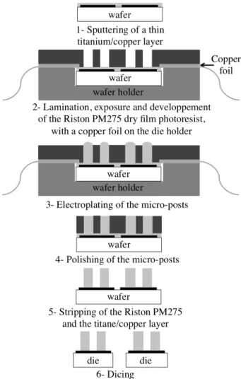
The process described here was presented in details in [6] for a single die. Here, we describe its application to a wafer. The different manufacturing steps to realize the MPI on a chip are presented in Figure 4. For the electroplating process, we worked on some pieces of wafer (5x5 diodes) with a surface of 6x6 mm for each diode. These pieces were cut from a 6 inch un-diced wafer sourced from a commercial manufacturer. The diodes have a classical finish (aluminium on top, silver on bottom).
Before the electroplating of the micro-posts, the top of the wafer must be covered with a thin titanium (Ti) / copper (Cu) layer (25nm/300nm respectively), as the pads are ready for wire bonding (Al finish). Diodes designed specifically for copper electroplating would suppress this primary preparation of the die. This preparation is obviously compatible with wafer-level process. By sputtering this layer, titanium is used as an adhesion layer and copper is employed as a conductive layer for the electroplating step. A second step is performed prior to the electrolytic growth of the micro-posts using a dry film photoresist (Riston PM275 [8]) mainly seen in the electronics industry to realize printed circuit boards [9]. The dry film photoresist is composed of a photoresist
Figure 4 Manufacturing process of the proposed interconnection
layer sandwiched between a polyethylene protective foil and a polyester support. It offers some benefits such as a simple process (lamination, exposure and development), a remarkable robustness to the acid bath, a decrease in the edge beads on the substrate, and a low cost. The dry film photoresist has a thickness of 75μm and a nominal resolution of 50μm. The process to realize the pattern in one layer of the Riston PM275 is the following. The polyethylene foil is removed. The photoresist is deposited by lamination on the wafer at 110°C. It is then exposed to an UV source through a mask for selective curing. After lamination and exposure, the polyester support is peeled away. Finally the photoresist is developed with a spray system in a sodium carbonate solution at 1% (5g of sodium carbonate diluted in 500ml of water) during 1min30s and with a processing temperature of 30°C. Figure 5 shows a wafer holder, with 5x5 diodes and a copper foil, laminated by a photoresist film, exposed and developed showing the micro-posts mold matrix. The experimental electrolytic cell that is used to deposit the copper micro-posts, has electrodes that are fixed horizontally. This configuration allows to obtain relatively homogeneous micro-posts over the surface of the wafer pieces. The electrolytic bath is an acid solution that is composed of pentahydrate copper sulphate (220g/l), sulphuric acid (32ml/l), hydrochloric acid
(0,2ml/l), and brightener and leveller additives (2ml/l of Rubin T200-A, 8ml/l of Rubin T200-G and 2ml/l of Rubin T200-E). Electroplating of the micro-posts is performed at ambient temperature with a typical current density of 10 mA/cm2. The experimental growth rate of
the micro-posts is linear and close to 11 μm/h [6], for a current density of 10 mA/cm2. This value is more
significant than the growth rate of metals deposited by sputtering or evaporation. The minimal deposit time has been set to 7h. Noted that growth rate may be increased so as to adjust to smaller deposit time. The deposit time achieves a micro-posts slightly higher than the thickness of the Riston PM275, and so allows then for a mechanical polishing and/or grinding step of the micro-posts in order to obtain a planar surface and ensure a good electrical and thermal contact between the micro-posts and the DBC substrate.
A mechanical polishing is realized thanks to a cloth polishing disk and a diamond liquid with grains of 9μm down to 1μm in the lab-scale experiment. The height of the micro-posts is 60 μm after polishing, and they have a square section of 900µmx900µm with a distance of 300µm between two micro-posts.
The following step consists in removing of the Riston PM275 photoresist film in a sodium hydroxide solution at 3% (15 g of sodium hydroxide diluted in 500 ml of water). Finally, in order to avoid short-circuiting the edge protections of the dies, the Ti/Cu layer is removed as followed: Cu layer was removed thanks to APS COPPER ETCHANT (about 1min), and Ti layer was removed by a 5% dilute HF (about 1s).
The last step is the dicing of the pieces of wafer into 5x5 diodes. It is performed on a Disco dicing saw (Figure 7a).
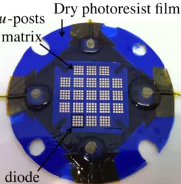
Figure 5 Photo of a wafer holder with 5x5 diodes and a copper foil laminated by the photoresist film, micro-posts matrix insulated and developed. The diameter of the wafer holder is 80 mm.
4
Results and discussion
4.1 Assembled MPI structure
The minimal working force permitted by our SPS equipment is 5 kN, which poses problems in regard to the
Figure 6 A photo the MPI structure in a graphite jig
Figure 7 A photo (a) of a diode (6x6 mm) with micro-posts on its top-side and (b) a SEM photo of DBC-did-DBC sandwich assembly achieved using the presented SPS process
small section of the micro-posts (13 mm² in the case of the diode depicted in figure 7a). This result in very high localized stresses (in the order of 400 MPa), and in the cracking of our die. To avoid this crack, the two DBC substrates and the die with the micro-posts on its topside were put together in a graphite jig with the same height (see Figure 6), in order to decrease the force experienced by the die. This setup was found to work correctly, but it must be noticed that due to the machining tolerances, and the stiffness of the graphite jig, the actual stress experienced by the die and the copper posts cannot be calculated.
Several DBC/die/DBC assemblies were performed in vacuum (10−2 torr) with temperatures ranging from 200
°C to 300 °C, a heating rate equal to 100°C/min, a time fixed to 5 min, and a pressure estimated to a few MPa. Figure 7 shows the diode with micro-posts on its topside (a) and a SEM cross-section of a DBC-diode-DBC sandwich assembly achieved using the presented SPS process (b). From figure 7b, we can see that the micro-posts were successfully bonded to DBC and the silver (backsides of the diode) was asdo bonded to the copper of the DBC.
4.2 Electrical characterization of MPI
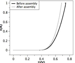
The electrical characterization of all the dies, forward and reverse I(V) characteristic, before and after assembly was performed using a keithley 2410 SMU in 4-probes setup. The measuring range was set to 1V-1A for forward characteristic and 300V-0,001A for reverse characteristic. This data shows no degradation of the characteristics of the dies. Figure 8 shows an I/V forward characteristics of a die assembled at 300°C. The lower resistance achieved after assembly is due to a better current spreading over the die surface.
Figure 8 Forward I(V) measurements acquired before (black line) and after (grey line) assembly.
Figure 9 Reverse I(V) measurements acquired before (black line) and after (grey line) assembly
Figure 9 presents an I/V reverse characteristics of the same die. The leakage current appears to be lower after assembly. This might be due to the change in the electric field distribution caused by the top DBC as compared to a wire bond. However, more accurate measurements are needed for the results presented here. A micro-amp resolution was considered sufficient to detect any damage to the die. To actually investigate this reduction in leakage current, a sub nano-amp resolution will be required (guarded measurements, controlled atmosphere…)
4.3 Discussion
The copper-to-copper bond in our MPI structure is not investigated, with the presence of the DBC ceramic layer, in order to be with the same parameters of bonding a copper-to-copper rod. The electroplated process is made in a collective way, using a wafer of 5x5 diode, compared to the wire bonding process that requires a single die work. Moreover, all these technology’s steps are standard (including polishing, which will be better in an industrial-scale). This structure is also able to assemble different dies with different thickness.
5
Conclusion
The paper presents the details of an alternative interconnection solution for power semiconductor dies that aims to be compatible with 3D integration of power modules. The different technology steps (electroplating, polishing and dicing) have been described. 3D DBC-Die-DBC assemblies using a SPS press have been successfully acheived. An electrical characterization shows that the diode has kept its integrity and a satisfying electrical connection is obtained showing no degradation of the die characteristic. Future work includes the production of a complete switching-cell for electrical transient characterizations and thermo-mechanical analysis (traction, shear and thermal cycling tests).
6
Acknowledgement
The authors would like to thank the Agence Nationale de la Recherche for their financial support of this work under the project grant ECLIPSE. They are also pleased to acknowledge important contributions used in the body of this work from G. Bonnefont and F. Mercier from MATEIS for SPS processing.
7
References
[1] K. Xing, F. C. Lee, and D. Boroyevich, “Extraction of parasitics within wire-bond IGBT modules,” in Applied Power Electronics Conference and Exposition, 1998. APEC ’98, Thirteenth Annual, 1 (1998) pp. 497-503
[2] M. Ciappa, “Selected failure mechanisms of modern power modules,” Microelectronics Reliability, 42 (2002) No. 4-5, pp. 653-667
[3] J. N. Calata, J. G. Bai, X. Liu, S. Wen, and G.-Q. Lu, “Three-Dimensional Packaging for Power Semiconductor Devices and Modules,” IEEE Transactions on Advanced Packaging, 28 (2005) No. 3, pp. 404-412
[4] X. He, X. Zeng, X. Yang, and Z. Wang, “A Hybrid Integrated Power Electronic Module Based On Pressure Contact Technology,” in Power Electronics Specialists Conference, PESC06, 37th IEEE (2006) pp. 1-5
[5] E. Vagnon, J. C. Crebier, Y. Avenas, and P. O. Jeannin, “Study and realization of a low force 3D press-pack power module,” in Power Electronics Specialists Conference, PESC08, IEEE (2008) pp. 1048-1054
[6] L. Ménager, M. Soueidan, B. Allard, V. Bley, and B. Schlegel, “A Lab-Scale Alternative Interconnection
Solution of Semiconductor Dice Compatible with Power Modules 3-D Integration,” IEEE Transactions on Power Electronics, 25 (2010) No. 7, pp. 1667-1670
[7] B. Mouawad et al., “Application of the Spark Plasma Sintering Technique to Low-Temperature Copper Bonding,” to be published in IEEE Transactions on Components and Packaging Technologies.
[8] Datasheet Dupont Platemaster PM200, Dupont, 2006
[9] E. Kukharenka, M. M. Farooqui, L. Grigore, M. Kraft, and N. Hollinshead, “Electroplating moulds using dry film thick negative photoresist,” Journal of Micromechanics and Microengineering, 13 (2003) No. 4, pp. s67-74
![Table 1 Measurement summary for different SPS experiments [7]](https://thumb-eu.123doks.com/thumbv2/123doknet/14369246.504084/3.892.448.804.660.850/table-measurement-summary-different-sps-experiments.webp)