HAL Id: hal-02267957
https://hal.archives-ouvertes.fr/hal-02267957
Submitted on 7 Oct 2020
HAL is a multi-disciplinary open access
archive for the deposit and dissemination of
sci-entific research documents, whether they are
pub-lished or not. The documents may come from
teaching and research institutions in France or
abroad, or from public or private research centers.
L’archive ouverte pluridisciplinaire HAL, est
destinée au dépôt et à la diffusion de documents
scientifiques de niveau recherche, publiés ou non,
émanant des établissements d’enseignement et de
recherche français ou étrangers, des laboratoires
publics ou privés.
Strong interlayer hybridization in the aligned
SnS2/WSe2 hetero-bilayer structure
Jihene Zribi, Lama Khalil, Biyuan Zheng, José Avila, Debora Pierucci,
Thibault Brulé, Julien Chaste, Emmanuel Lhuillier, Maria Asensio, Anlian
Pan, et al.
To cite this version:
Jihene Zribi, Lama Khalil, Biyuan Zheng, José Avila, Debora Pierucci, et al.. Strong interlayer
hybridization in the aligned SnS2/WSe2 hetero-bilayer structure. npj 2D Materials and Applications,
Nature, 2019, 3 (1), �10.1038/s41699-019-0109-3�. �hal-02267957�
1
Strong Interlayer Hybridization in the aligned
SnS2/WSe2 Hetero-bilayer Structure
Jihene Zribi1*, Lama Khalil1*, Biyuan Zheng2, José Avila3, Debora Pierucci4, Thibault Brulé5, Julien Chaste1,
Emmanuel Lhuillier6, Maria C. Asensio7, Anlian Pan2||, and Abdelkarim Ouerghi1|| 1Centre de Nanosciences et de Nanotechnologies, CNRS, Univ. Paris-Sud, Université Paris-Saclay
10 Boulevard Thomas Gobert, 91120 Palaiseau, France
2Key Laboratory for Micro-Nano Physics and Technology of Hunan Province, State Key Laboratory of
Chemo/Biosensing and Chemometrics, and School of Physics and Electronics, Hunan University, Changsha, 410082 Hunan, China
3Synchrotron-SOLEIL, Saint-Aubin, BP48, F91192 Gif sur Yvette Cedex, France
4CELLS - ALBA Synchrotron Radiation Facility, Carrer de la Llum 2-26, 08290 Cerdanyola del Valles,
Barcelona, Spain
5HORIBA France SAS, Passage Jobin Yvon, Avenue de la Vauve, 91120 Palaiseau, France 6 Sorbonne Université, CNRS, Institut des NanoSciences de Paris, INSP, F-75005 Paris, France
7Instituto de Materiales de Madrid, CSIC, C/ Sor Juana Inés de la Cruz, 3
Cantoblanco, 28049 Madrid, Spain
* These authors contributed equally to this work. || Corresponding authors E-mails:
Abstract
The combination of monolayers of different two-dimensional materials into van der Waals hetero-bilayer structures creates unprecedented physical phenomena, acting as a powerful tool for future devices. Understanding and exploiting these phenomena hinge on knowing the electronic structure and the hybridization of hetero-bilayer structures. Here, we show strong hybridization effects arising between the constitutive single layers of a SnS2/WSe2 hetero-bilayer structure grown by chemical vapor deposition. Surprisingly, the valence band maximum
position of WSe2 is moved from the K point for the single layer WSe2 to the Γ point for the aligned SnS2/WSe2
hetero-bilayer. Additionally, a significant photoluminescence quenching is observed for the SnS2/WSe2
hetero-bilayer structure with respect to the WSe2 monolayer. Using photoluminescence spectroscopy and
nano-angle-resolved photoemission spectroscopy techniques, we demonstrate that the SnS2/WSe2 heterostructure present a
type-II band alignment. These findings directly answer many outstanding questions about the electronic band structure and the band offset of SnS2/WSe2 hetero-bilayers for envisaging their applications in nanoelectronics.
2
Two-dimensional (2D) layered semiconductors with few atomic layer thicknesses and tunable bandgaps have attracted a significant interest in the last years. Particularly, 2D transition metal dichalcogenides (TMDs) (e.g. tungsten diselenide WSe2) possess a high carrier mobility1 and several spin properties,2,3,4 and are made of an
ordered stacking of building blocks. These 2D TMD materials constitute promising candidates for the study of novel physical phenomena and functionalities in electronics,4 photonics and superconductivity.5 By combining
individual monolayers (MLs) of different 2D layered materials in a van der Waals (vdW) heterostructure, presenting sharp interfaces at the atomic scale, one can tailor the energy band alignment. This opens up vast opportunities for fundamental investigations of novel electronic and optical properties. Therefore, most of the recent research in the field of 2D TMDs has been focused on TMDs/TMDs or TMDs/graphene heterostructures.6,7
Among the 2D materials, tin disulfide (SnS2) has an atypical band structure, being a IV-VI semiconductor in which
each layer of Sn atoms is sandwiched between two layers of S atoms; the weakly coupled layers in SnS2 interact
with each other through vdW interactions. Note that SnS2 is an earth-abundant, and a low-cost and an
environmentally friendly material. In its bulk form, SnS2 is extensively studied mostly for photovoltaics.8 As a 2D
TMD, SnS2 is interesting since it exhibits high carrier mobility9,10 and a strong excitonic effect (binding energy of
~0.9 eV for a single layer).11 The electronic band structure of SnS
2 has been investigated in several DFT studies
showing that in contrast to TMDs, the indirect to direct band gap transition for SnS2 does not occur from bulk
down to a single layer.11,12 This has been experimentally confirmed by Huang et al12 through layer-dependent
photoluminescence (PL) and band structure measurements of bulk SnS2. However, the electronic band structure
of a single layer of SnS2 has not been measured yet.
The SnS2/WSe2 hetero-bilayers have started to attract a great attention,13 in order to combine the various
characteristics of SnS2 and WSe2 single layers. Different methods have been used to obtain this heterostructure.
For example, mechanically exfoliated few-layer/few-layer stacked WSe2/SnS2 heterostructures with an
anti-ambipolar behavior have been reported by Wang et al.14 In addition, Zhang et al.15have demonstated the possibility
of growing few layers of WSe2 on micro-plates of SnS2 randomly oriented. More recently, Yang et al.13 have
employed a two-step vapor phase route to grow WSe2/SnS2 flakes, having the largest size of atomic layered vertical
heterostructures with a lateral size reaching up the millimeter scale. According to its band alignment, 2H-SnS2
/2H-WSe2 is a type II heterostructure characterized by the high efficiency of charge separation14,16. Devices based on
this type of vdW heterostructures have shown improved optoelectronic performances.16 Note that electrical
transport measurements and optical characterizations have revealed that the direct growth of high-quality vdW heterostructures is promising for the obtainment of high-performance integrated optoelectronic devices.13
In order to realize vdW heterostructures promoted by weakly bonded layered structure of these 2D materials, mechanical exfoliation has been largely used as one of the most appropriate fabrication techniques. However, by using this method, the stacking orientation cannot be precisely controlled and the interface is easily contaminated.17,18 To avoid these limitations, chemical vapor deposition (CVD) is employed as an alternative
growth method for the scalable synthesis of high-quality atomic layered vdW heterostructures with well-defined interlayer orientations and clean interfaces. In this paper, we probe the electronic structure of the hetero-bilayer SnS2/WSe2 heterostructure, grown via the CVD technique, with microscopic Raman (µ-Raman)/PL spectroscopy
3
and nano angle-resolved photoemission spectroscopy (nano-ARPES). For this heterostructure, a type II band alignment was measured with an interfacial optical bandgap of about 1.65 eV. Since it is straightforward to evaluate if the constitutive single layers of the heterostructure retain their electronic properties after the layer stacking or they are strongly perturbed, we have investigated the punctual band structure of selected areas on our sample. Specifically, we have provided a precise electronic characterization for the WSe2 single layer and the
SnS2/WSe2 hetero-bilayer structures, which are actually simultaneously present on the same flake after the growth.
For the first time, through our nano-ARPES measurements, we provide a direct experimental evidence of a strong electronic band hybridization for the aligned SnS2/WSe2 heterostructure. In particular, we demonstrate that the
valence band maximum (VBM) of WSe2 changes its position in the Brillouin zone (BZ) from the K to the point
when moving from the single layer to the hetero-bilayer structure. A significant PL quenching was also observed for the SnS2/WSe2 hetero-bilayer structure with respect to the WSe2 monolayer.
Results and Discussion
2H-SnS2/2H-WSe2 heterostructures were grown via two-step CVD (see Materials and Methods and ref13). Single
layer WSe2 flakes were first grown on SiO2/Si substrates. Then, these structures were used as templates for the
subsequent growth of single layers of SnS2 to form the vertical hetero-bilayer structures of SnS2/WSe2. A
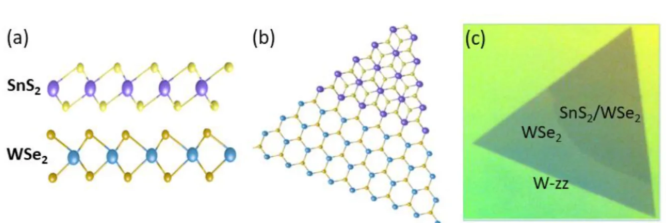
schematic side and top views of the atomic structure of the flakes are presented in Figures 1(a) and (b), respectively. The large lattice mismatch between SnS2 and WSe2 (14.3%) indicates that the bonding between adjacent layers is
principally of the vdW type.19,20 This lattice mismatch leads to a periodic variation of atomic registry between
individual van der Waals layers, exhibiting a Moiré pattern with a well-defined periodicity. Figure 1(c) illustrates a typical zoomed-in optical image of one flake, in which the formation of the SnS2/WSe2 hetero-bilayer is clearly
visible. The thickness of the triangular crystals was determined by the height profiles obtained from atomic force microscopy (AFM) (see Figures 1(d) and (e)).13 Based on the optical image, we can clearly conclude that
atomically thin flakes, possessing triangular shapes and sharp edges, are formed on top of the SiO2/Si substrate
through the CVD process. These triangular flakes are only composed of one edge termination, namely, the W-zz termination.21 It should be pointed out that truncated triangular flakes can also be readily detected on the edges of
our specimens. This modification in the shape of the flakes is a common phenomenon for the single layer of 2D materials synthetized by means of the CVD method,22,23 and is mainly due to structural differences in the edges of
the flakes and to the local difference in the growth rates.22 It is noteworthy that the irregular evolution of the SnS 2
edge with respect to WSe2 edgecould be related to the presence of distinct seeding centers, which affect the growth
kinetics of the CVD growth of SnS2 on WSe2.24
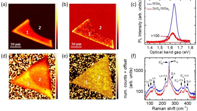
To probe the details of light emission obtained from the WSe2 and SnS2/WSe2 domains, µ-PL spectroscopy was
carried out on the microscopic flake of Figure 1(c), using a 532 nm laser excitation. The measured PL maps and spectra are reported in Figure 2. In Figures 2(a) and (b), we present PL intensity and peak position mapping images obtained from the triangular flake with their corresponding intensity and energy scales on the right, respectively. At first sight, we clearly remark that the WSe2 regions reveal a higher PL intensity than the SnS2/WSe2
hetero-bilayer domains (Figure 2(a)). This is confirmed by comparing their corresponding PL spectra obtained from two specific points 1 and 2 representative of the distinct regions (see Figure 2(c)). Actually, for the SnS2/WSe2
4
theintensity of the peaks differs at least by a factor of 200. This significant PL quenching could be related to an interlayer interaction between SnS2 and WSe2, which leads to a strong photo-induced electron transfer from WSe2
to SnS2,25,26 hindering the recombination of electron-hole pairs created by the photoexcitation. Another more
probable scenario explaining the PL quenching is a predicted WSe2 bandgap transition from a direct to an indirect
gap after the increase of the number of layers. This strongly affects the PL emission, as in our case. Since the interlayer coupling in our clean heterostructure is very strong due to the perfect crystalline orientation4, a ruthless
modification of the WSe2 electronic band structure could lead to the appearance of an indirect bandgap, providing
this PL intensity drop (this will be further discussed in the next paragraphs).
To learn more about the electronic properties of the SnS2/WSe2 hetero-layer structure, we have conducted a
µ-Raman spectroscopy study. This technique has been widely used to study 2D materials, in order to determine the number and the stacking sequence of layers, as well as the external field, the molecular doping and the strain effects. Figures 2(d) and (e) show the respective µ-Raman peak position and intensity mapping images of the as-grown triangular flake of Figure 2(a), acquired at room temperature with a 532 nm laser excitation. These maps reveal that a downshift of the peak positions and a slight variation in the peak intensities are observed when moving to the SnS2/WSe2 hetero-bilayer region. Moreover, in Figure 2(f), we present Raman spectra taken from two
different points labeled 1 and 2 on the WSe2 and the SnS2/WSe2 domains. Beside the first order modes in the center
of the BZ: the in-plane phonon mode 𝐸2𝑔1 , expected at 206 cm-1 for SnS211 and at 249.5cm-1 for WSe2, and the
out-of-plane phonon mode A1g, expected at 305 cm- 1 for SnS2 and at 249.5 cm- 1 for WSe2 (𝐸2𝑔1 and A1g are degenerated
modes for WSe2 single layer), the Raman spectra present a series of overtone and combination peaks.27 In
particular, we notice in our measurements the ZA(M) at 109 cm-1 or the TA(M) expected at 100 cm-1, the LA(M)
at 133 cm-1, a Raman mode due to LA phonons at the M point of the BZ zone, the combination of LA(M) and
TA(M) at 227 cm-1, the second order harmonic 2LA (M) mode at 266 cm-1, and the third order LA(M) mode at
401 cm-1. Additionally, we can detect Raman peaks at 352 cm-1 and 378 cm-1, which constitute combination modes
between LA(M), TA(M) or ZA(M), with E1
2g (Γ) modes. From the Raman spectra of Figure 2(f), we can conclude
that the Raman peak amplitude obtained from SnS2 single layer is expected to be negligible. However, after long
time integration, a small peak, visible at 310 cm-1 (inset in Figure 2(f)) and attributed to the A
1g mode of SnS2, is
detected. The presence of this peak confirms the PL results, where a negligible intensity of the PL peak has been identified for the SnS2/WSe2 hetero-bilayer structure. Besides, for the latter structure, the main WSe2 Raman peak
is redshifted by an amount of 0.3 cm-1 toward lower frequencies with respect to the peak of ML structure, similarly
to the PL peak, which also exhibits a downshift of almost 20 meV for the optical band gap. It should be pointed out that we were not able to provide any clear evidence of an efficient charge transfer through Raman spectroscopy.
Further information on the electronic structure of the SnS2/WSe2 hetero-bilayer could be carried out by performing
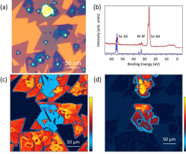
nano X-ray photoemission spectroscopy (nano-XPS) measurements. It is worth noting that the CVD-grown flakes are transferred onto graphene/SiC substrates, in order to avoid problems related to charging effect that could occur when using other substrates like SiO2/Si.28 Therefore, graphene/SiC substrates are very appropriate for XPS
and ARPES investigations.29,30 Figure 3(a) shows an optical image of the probed region on the sample, which
contains the flakes. Wide XPS spectra, acquired on both the WSe2 single layer and the SnS2/WSe2 hetero-bilayer
5
photoemission yields of both regions, we can clearly detect the presence of an additional peak, namely, the Sn 4d shallow core level for the SnS2/WSe2 hetero-bilayer (red curve) with respect to the WSe2 single layer (blue curve).
By integrating the photoemission intensity within two selected energy windows around the W 4f and Sn 4d peaks, while scanning the sample along two in-plane directions, we generate the element-specified core level intensity distribution images (see Figure 3(c) and (d), respectively). Hence, Figure 3(c) shows a spatially resolved map of W 4f, revealing the presence of triangular flakes corresponding to the WSe2 ML domains: as can be clearly noticed,
areas where the intensity is higher represent the MLs of WSe2 that have not been covered with SnS2, while areas
where the intensity is lower correspond to regions rich in SnS2. On the contrary, the spatially resolved map of Sn
4d, shown in Figure 3(d), presents a reversed intensity contrast with respect to the map of Figure 3(c), revealing
SnS2 regions that partially cover the WSe2 flakes. This confirms what was already observed in the optical image
of in Figure 1(c). Therefore, these core level images evidently prove that we were able to localize with a nanometric spatial resolution the WSe2/SnS2 heterostructure, which allows us to study the electronic band structure of the
system.
To study the correlation between the layer structure of the flakes (i.e. WSe2 single layer or WSe2/SnS2
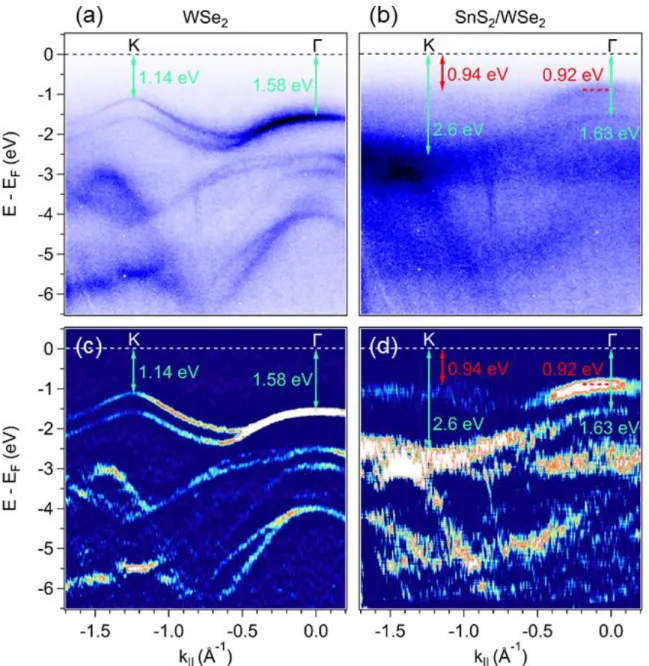
hetero-bilayer) and the electronic band structure, we have employed the nano-ARPES technique. Figures 4(a) and (b) present the photoelectron intensity maps acquired on WSe2 single layers and on SnS2/WSe2 hetero-bilayers,
respectively at 100 eV. In order to enhance fine spectral features and get better clarity of the band structure presented in Figures 4(a) and (b), the second derivatives of the photoelectron intensity as a function of binding energy and parallel wave vector were also provided in Figures 4(c) and (d). Note that previous transmission electron microscope measurements have shown that SnS2 and WSe2 domains present the same orientation.31 The
alignment within this type of heterostructures is an important factor for nano-ARPES studies since it allows performing measurements along the same high-symmetry direction, i.e. along Γ-K, in the hexagonal BZ for both WSe2 and SnS2/WSe2 layers. From the ARPES yields in Figures 4(a) and (b), we clearly detect the layer-dependent
band structure evolution: in particular, moving from the WSe2 ML film to the WSe2/SnS2 hetero-bilayer structure,
we can see that the VBM located at the K point (1.14 eV binding energy) for the WSe2 single layer switches to the
point (1.63 eV binding energy) for the WSe2/SnS2 hetero-bilayer. In addition, the nano-ARPES measurements
also reveal features related to the band structure of SnS2 single layer (see Figure 4(b)), which are located at 0.92
eV and 0.94 eV binding energy bellow the Fermi level at the Γ and K points, respectively. One should note that the SnS2 band structure obtained from our nano-ARPES data is in a good agreement with the one calculated for
SnS2 single layer by Huang et al.12
For the WSe2 single layer films, we remark that the VBM is significantly higher than the maximum of the band
located at the point (the difference between these maxima has an amount of 0.44 eV), and that the bands are remarkably sharp, indicating the high quality of the flakes. Moreover, for the WSe2 ML case, the strong spin orbit
coupling (SOC) of the d-orbitals leads to an energy splitting of the valence band at the K point in the BZ, and thus the spin degeneracy is lifted by the inversion symmetry breaking. This induces a spin-polarization of the bands. Based on the ARPES data, the directly extracted value of the SOC energy splitting is equivalent to 480 meV, consistent with previous values experimentally measured in previous studies.32,33 In the hetero-bilayer structure
(Figures 4(b) and (d)), the main feature indicating the band structure variation of WSe2 is the change in the VBM
6
extremely different from the bands of the single layer, thereby implying a strong interlayer hybridization effect between SnS2 and WSe2; this was previously observed also for the WSe2 homo-bilayer structure. Consequently,
this strong band interaction, coming from the heterostructure formation, pulls up the energy level of the valence band located at the Γ point at 1.63 eV binding energy bellow the Fermi level) and pushes down the conduction band energy level positioned at the K point. This may later explain the type II band alignment in the aligned hetero-bilayer. Although SnS2 is covering the WSe2 layer, the employed photon energy of 100 eV allows to detect
photoelectrons from WSe2 after constructing the heterostructure. This is due to thepenetration depth of the beam
that allows to probe more than a bilayer structure.34 Consequently, the strong signal attenuation observed in our
ARPES intensity maps at the K point is not due to screening effects, which make the electronic structure less visible, but to a strong hybridization effect between SnS2 and WSe2. Besides, it is instructive to compare our
ARPES results with the projected band structure of the 2H-WSe2/2H-SnS2 heterostructure, obtained theoretically
via first-principle calculations by Wang et al.14 Even though SnS
2 is lying on the bottom and WSe2 above in the
latter study, we observe an electronic band structure of WSe2 similar to the one shown in our photoelectron
intensity maps in Figure 4(b): the VBM of the heterostructure, located at the Γ point, is higher than the maximum of the valence band at the K point. Nevertheless, in contrast to our results, SnS2 is behaving more n-type as
compared to WSe2. This can be attributed to the choice of the substrate: in fact, in our experiment, we have used
a graphene/SiC(0001) substrate, which is different from the one employed by Wang et al. By changing the substrate, one can tune the position of the Fermi level in the heterostructure. Thus, the substrate has not a direct effect on the scenario of hybridization of the atop materials, but rather participates in the charge transfer process, which affects the doping of the atop layers. Additionally, one should note that, even though the CVD process introduces considerable defects density in 2D materials, the growth of a second layer with a different chalcogen atom would not have healing effect on the first layer. To the best of our knowledge, when the deposition temperature in the second CVD process is above 750 °C, the reaction between S atoms in atmosphere and Se atoms in WSe2 will actually occur.35 However, in our second CVD process, the growth temperature was deliberately
chosen to be 600 °C, and thus the WSe2 layer is stable. Besides, a previous study conducted by Li et al.36 on WSe2
-MoS2 lateral heterostructures has showed that the order for material growth, that is, WSe2 first and MoS2 second,
is important to avoid the ionic exchange of Se-S occurring above 800 °C. The STEM measurements performed on WSe2-MoS2 confirmed that the lateral interface is atomically sharp and that there is no signature of Mo-W and
Se-S bond formation in a micrometer range in parallel to the junction. Consequently, the optical signals as well as the electronic structure obtained in the present study are not affected by the growth of a layered material with two distinct chalcogen atoms.
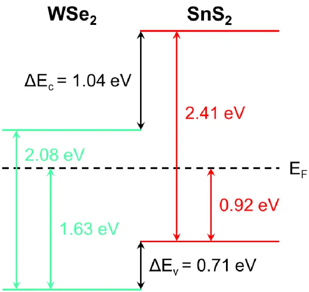
Based on our nano-ARPES results and on literature, we have determined the band alignment of the SnS2/WSe2
system (see Figure 5), in which the electronic band gaps of WSe2 and SnS2 are 2.08 eV37 and 2.41 eV11,
respectively. The valence band and conduction band offset values are determined to be 0.71 and 1.04 eV, respectively, with type II band alignment having the advantage of electron-hole pair separation. This efficient charge separation in the SnS2/WSe2 heterostructure can clarifythe quenching observed in the PL peak of Figure
2(c). Consequently, these observations, revealing that the band alignment is of type II, are significant for future technological electronic and opto-electronic applications since type II heterostructures facilitate the efficient electron-hole separation for light detection.
7
Therefore, our nano-ARPES results on the SnS2/WSe2 heterostructure report a strong hybridization between WSe2
and SnS2, which is evident from the change of the VBM position of WSe2 from the K point in the pristine sample
to the Γ point in the hetero-bilayer structure due to the strong interlayer coupling. Even though not all the aspects related to the genuine determination of the conduction band minimum (CBM) of WSe2 in the hetero-bilayer
system are clear, we suggest that WSe2 may probably exhibit a band gap transition from a direct to an indirect
gap, confirmed by the PL quenching observed for the SnS2/WSe2 hetero-bilayer. This expected band gap
transition to an indirect gap was observed by Wang et al.14 in their first-principle calculations of the electronic
band structure of the 2H-WSe2/2H-SnS2 heterostructure. In addition, a probable photo-induced charge transfer,
involving electrons from the CBM of WSe2 and holes from the VBM of SnS2, could also contribute to the
quenching observed in the PL measurements.
In summary, we have studied the electronic structure of the SnS2/WSe2 hetero-bilayer structure. A detailed
investigation by means of µ-PL and nano-ARPES allowed us to extract the band alignment of this heterostructure, revealing that it has a type II configuration with an interfacial optical gap of 1.65 eV. A significant PL quenching was observed for the SnS2/WSe2 hetero-bilayer structure with respect to the WSe2 ML, suggesting that WSe2 may
probably present a band transition from a direct to an indirect gap or/and a possible photo-induced charge transfer. In perspective, further time-resolved ARPES experiments and doping strategies, like for instance with potassium38 are required to study in detail the unoccupied states of the SnS
2/WSe2 hetero-bilayer structure in order
to verify the probable band gap transition. Our findings demonstrate the possibility of band structure engineering of TMDs, by taking advantage of the strong hybridization effects occurring between the constitutive single layers of the heterostructure, as in the case of the SnS2/WSe2 hetero-bilayer structure.
Methods
Growth and Transfer of SnS2/WSe2:The SnS2/WSe2 heterostructures were grown through a two-step chemical
vapor deposition process. Firstly, to grow WSe2 monolayers, tungsten diselenide powder was placed at the center
of a furnace and SiO2/Si substrate was placed at the downstream of a quartz tube. Then, the argon carrier gas flow
rate was fixed at 50 sccm and the temperature was increased to 1100 °C and maintained stable for 10 minutes. The as-synthesized WSe2 monolayers were, subsequently, used as templates for the growth of SnS2. S powder, SnO2
powder and as-grown WSe2 monolayers on SiO2/Si substrate were placed at the upstream, center and downstream
of the quartz tube, respectively. Thereafter, the argon carrier gas flow rate was fixed at 50 sccm at a pressure of 8 Torr and the temperature was increased to 600 °C and kept stable for 8 minutes. After the growth, the furnace was cooled down to room temperature. The SnS2/WSe2 flakes transferred onto graphene39,40, retain their triangular
shapes with unchanged lateral sizes. Before any measurement, the sample was annealed at 250 °C for 60 min in ultrahigh vacuum, in order to remove the residual surface contaminations induced by the wet transfer.
Single layer Graphene on SiC(0001): Single layer graphene was produced following a two-step thermal heating growth process of SiC(0001) substrate. Before the graphitization, the substrate was etched with hydrogen (100% H2) at 1550 °C to produce well-ordered atomic terraces of SiC. Afterwards, the SiC substrate was heated to 1000
8
Micro-Raman and Photoluminescence Spectroscopy: The micro-Raman and photoluminescence measurements were conducted using a commercial confocal HORIBA LabRAM HR Evolution micro-Raman microscope operating at 532 nm and 633 nm. The incident photon beam was focused down to a submicrometric spot (~0.5 µm in diameter) on the sample. The incident power was ~0.1 mW. All measurements were performed at room temperature with the same microscope using a 100× objective and a CCD detector (detection range between 1.2 eV and 6.2 eV).
Angle-Resolved Photoemission Spectroscopy: The nano-ARPES experiments were performed at the ANTARES beamline of the SOLEIL synchrotron light source (Saint-Aubin, France). The ARPES data were taken at a photon energy of 100 eV, using linearly polarized light. All measurements were carried out at a base pressure of 5 × 10⁻¹¹ mbar and a base temperature of 70 K.
Data Availability
The datasets generated during and/or analysed during the current study are available from the corresponding author on reasonable request.
Acknowledgements
We acknowledge the financial support by RhomboG (ANR-17-CE24-0030) grants. This work is supported by a public grant overseen by the French National Research Agency (ANR) as part of the “Investissements d’Avenir” program (Labex NanoSaclay, reference: ANR-10-LABX-0035).
Competing Interests
The authors declare no competing interests.
Author Contributions
B. Z. and A. P. fabricated the samples. J. Z., D. P., A. O., J. A. and M. C. A. carried out the nano-XPS/nano-ARPES experiments. J. C., A. O. and T. B. characterized the samples by means of µ-Raman/PL spectroscopy and analyzed the Raman/PL data. J. Z., T. B., J. C., L. K., J. A., D. P. and E. L. analyzed the data. J. Z. and L. K. wrote the manuscript under the supervision of A.O. All the authors discussed the results and commented on the manuscript.
References
1. Radisavljevic, B., Radenovic, A., Brivio, J., Giacometti, V. & Kis, A. Single-layer MoS2 transistors. Nat.
Nanotechnol. 6, 147–150 (2011).
2. Xiao, D., Liu, G.-B., Feng, W., Xu, X. & Yao, W. Coupled Spin and Valley Physics in Monolayers of MoS2 and Other Group-VI Dichalcogenides. Phys. Rev. Lett. 108, 196802 (2012).
3. Mak, K. F., He, K., Shan, J. & Heinz, T. F. Control of valley polarization in monolayer MoS2 by optical
helicity. Nat. Nanotechnol. 7, 494–498 (2012).
4. Zeng, H., Dai, J., Yao, W., Xiao, D. & Cui, X. Valley polarization in MoS2 monolayers by optical
pumping. Nat. Nanotechnol. 7, 490–493 (2012).
5. Cao, Y. et al. Unconventional superconductivity in magic-angle graphene superlattices. Nature 556, 43– 50 (2018).
9
6. Fang, H. et al. Strong interlayer coupling in van der Waals heterostructures built from single-layer chalcogenides. Proc. Natl. Acad. Sci. 111, 6198–6202 (2014).
7. Lee, C.-H. et al. Atomically thin p–n junctions with van der Waals heterointerfaces. Nat. Nanotechnol. 9, 676–681 (2014).
8. Parkinson, B. A. Dye sensitization of van der Waals surfaces of tin disulfide photoanodes. Langmuir 4, 967–976 (1988).
9. Huang, Y. et al. Highly sensitive and fast phototransistor based on large size CVD-grown SnS2
nanosheets. Nanoscale 7, 14093–14099 (2015).
10. De, D. et al. High on/off ratio field effect transistors based on exfoliated crystalline SnS2
nano-membranes. Nanotechnology 24, 025202 (2013).
11. Gonzalez, J. M. & Oleynik, I. I. Layer-dependent properties of SnS2 and SnSe2 two-dimensional
materials. Phys. Rev. B 94, 125443 (2016).
12. Huang, Y. et al. Tin Disulfide—An Emerging Layered Metal Dichalcogenide Semiconductor: Materials Properties and Device Characteristics. ACS Nano 8, 10743–10755 (2014).
13. Yang, T. et al. Van der Waals epitaxial growth and optoelectronics of large-scale WSe2/SnS2 vertical
bilayer p–n junctions. Nat. Commun. 8, 1906 (2017).
14. Wang. Y. et al. Light induced double ‘on’ state anti-ambipolar behavior and self-driven photoswitching in p-WSe2/n-SnS2 heterostructures. 2D Mater. 4, 025097 (2017).
15. Zhang, X. et al. Vertical Heterostructures of Layered Metal Chalcogenides by van der Waals Epitaxy.
Nano Lett. 14, 3047–3054 (2014).
16. Zhou, X. et al. Tunneling Diode Based on WSe2/SnS2 Heterostructure Incorporating High Detectivity
and Responsivity. Adv. Mater. 30, 1703286 (2018).
17. Haigh, S. J. et al. Cross-sectional imaging of individual layers and buried interfaces of graphene-based heterostructures and superlattices. Nat. Mater. 11, 764–767 (2012).
18. Yang, W. et al. Epitaxial growth of single-domain graphene on hexagonal boron nitride. Nat. Mater. 12, 792–797 (2013).
19. Gong, Y. et al. Vertical and in-plane heterostructures from WS2/MoS2 monolayers. Nat. Mater. 13,
1135–1142 (2014).
20. Li, B. et al. Direct Vapor Phase Growth and Optoelectronic Application of Large Band Offset SnS2/MoS2 Vertical Bilayer Heterostructures with High Lattice Mismatch. Adv. Electron. Mater. 2,
1600298 (2016).
21. Ly, T. H., Yun, S. J., Thi, Q. H. & Zhao, J. Edge Delamination of Monolayer Transition Metal Dichalcogenides. ACS Nano 11, 7534–7541 (2017).
22. Wang, S. et al. Shape Evolution of Monolayer MoS2 Crystals Grown by Chemical Vapor Deposition.
Chem. Mater. 26, 6371–6379 (2014).
23. Wang, L., Chen, F. & Ji, X. Shape consistency of MoS2 flakes grown using chemical vapor deposition.
Appl. Phys. Express 10, 065201 (2017).
24. Zhu, D. et al. Capture the growth kinetics of CVD growth of two- dimensional MoS2. npj 2D Mater.
Appl. 1, 8 (2017).
25. Yu, Y. et al. Equally Efficient Interlayer Exciton Relaxation and Improved Absorption in Epitaxial and Nonepitaxial MoS2/WS2 Heterostructures. Nano Lett. 15, 486–491 (2015).
26. Hu, P. et al. Control of Radiative Exciton Recombination by Charge Transfer Induced Surface Dipoles in MoS2 and WS2 Monolayers. Sci. Rep. 6, 24105 (2016).
27. Zhao, W. et al. Lattice dynamics in mono- and few-layer sheets of WS2 and WSe2. Nanoscale 5, 9677–
9683 (2013).
28. Henck, H. et al. Direct observation of the band structure in bulk hexagonal boron nitride. Phys. Rev. B 95, 085410 (2017).
29. Henck, H. et al. Electrolytic phototransistor based on graphene-MoS2 van der Waals p-n heterojunction
with tunable photoresponse. Appl. Phys. Lett. 109, 113103 (2016).
30. Pierucci, D. et al. Band Alignment and Minigaps in Monolayer MoS2-Graphene van der Waals
Heterostructures. Nano Lett. 16, 4054–4061 (2016).
31. Yang, T. et al. Van der Waals epitaxial growth and optoelectronics of large-scale WSe2/SnS2 vertical
bilayer p–n junctions. Nat. Commun. 8, 1906 (2017).
32. Klots, A. R. et al. Probing excitonic states in suspended two-dimensional semiconductors by photocurrent spectroscopy. Sci. Rep. 4, 6608 (2014).
33. Riley, J. M. et al. Direct observation of spin-polarized bulk bands in an inversion-symmetric semiconductor. Nat. Phys. 10, 835–839 (2014).
34. Wilson, N. R. et al. Determination of band offsets, hybridization, and exciton binding in 2D semiconductor heterostructures. Sci. Adv. 3, e1601832 (2017).
10
36. Li, M.-Y. et al. Epitaxial growth of a monolayer WSe2-MoS2 lateral p-n junction with an atomically
sharp interface. Science (80-. ). 349, 524–528 (2015).
37. Chiu, M.-H. et al. Determination of band alignment in the single-layer MoS2/WSe2 heterojunction. Nat.
Commun. 6, 7666 (2015).
38. Alidoust, N. et al. Observation of monolayer valence band spin-orbit effect and induced quantum well states in MoX2. Nat. Commun. 5, 4673 (2014).
39. Henck, H. et al. Electronic band structure of Two-Dimensional WS2/Graphene van der Waals
Heterostructures. Phys. Rev. B 97, 155421 (2018).
40. Sediri, H. et al. Atomically Sharp Interface in an h-BN-epitaxial graphene van der Waals Heterostructure. Sci. Rep. 5, 16465 (2015).
Figure Legends
Figure 1: Crystal structure, and optical and AFM images of WSe2 single layer and SnS2/WSe2
hetero-bilayer: Schematic a) side and b) top views of the atomic structure of the vertically stacked SnS2/WSe2 vdW
heterostructure. c) A zoomed-in optical image of one flake, in which the formation of the SnS2/WSe2 hetero-bilayer
is clearly visible. (d) AFM image of the SnS2/WSe2 heterostructure. (e) The height profile indicates that the
thickness of the heterostructure is 1.6 nm (1ML WSe2 +1ML SnS2). The AFM study shows the successful
11
Figure 2: Photoluminescence and Raman spectroscopy on the heterostructure: a) and b) PL intensity and peak position mapping images obtained from the as-grown triangular flake in Figure 1(c) and acquired with a 532 nm laser excitation. c) Typical PL spectra, obtained from the WSe2 ML region (blue curve) and from the
SnS2/WSe2 hetero-bilayer domain (red curve). The PL intensity acquired from the SnS2/WSe2 hetero-bilayer
structure has multiplied by a factor of 100 in order to visualize the signal. d) and e) µ-Raman peak position and intensity maps of the same flake, acquired at room temperature with a laser beam generating 532 nm photons. f) Typical Raman spectra taken from WSe2 (blue curve) and the SnS2/WSe2 hetero-bilayer (red curve). Inset: Raman
spectrum obtained after a long time integration on the SnS2/WSe2 hetero-bilayer domain. A small peak, visible at
310 cm-1 and attributed to the A
12
Figure 3: Nano-XPS maps of the SnS2/WSe2 heterostructure: a) Optical image of a probed region on the
specimen, which contains the flakes. b) XPS survey spectra, acquired on both the WSe2 single layer (blue curve)
and the SnS2/WSe2 hetero-bilayer (red curve) with a photon energy of 100 eV. c) Typical W 4f integrated intensity
map, revealing the WSe2 ML domains marked in orange intensity color scale. d) Sn 4d integrated intensity image,
presenting a reversed intensity contrast with respect to the map of Figure 3(c); the SnS2 regions that partially cover
13
Figure 4: Comparison of the electronic band structure between the WSe2 single layer and the SnS2/WSe2
hetero-bilayer: a) and b) nano-ARPES images acquired on WSe2 single layers and on SnS2/WSe2 hetero-bilayers,
and taken at a photon energy of 100 eV along the ΓK high symmetry direction. (c) and (d) The second-derivative spectra of the maps in (a) and (b), respectively, exhibiting better visibility of the bands. The Fermi level, located at 0 eV binding energy, was determined by fitting the leading edge of the graphene layer.
14
Figure 5: Schematic of band alignment diagram of the SnS2/WSe2 heterostructure, obtained from nano-ARPES
measurements. The valence band maximum and conduction band minimum offset values are determined to be 0.71 and 1.04 eV, respectively, with type II band alignment.