Electrical characterization of advanced FDSOI CMOS
devices
Caractérisation électrique des Dispositifs CMOS FDSOI avancés
G. Ghibaudo1
1 IMEP-LAHC, Univ. Grenoble Alpes, Minatec/INPG, 3 Parvis Louis Neel, 38016 Grenoble, France, ghibaudo@minatec.inpg.fr
ABSTRACT. FDSOI technologies are very promising candidates for future CMOS circuits as they feature low variability, improved short channel effect and good transport characteristics. In this paper, we review the main electrical techniques and methodologies used to characterize the important MOS device parameters. First, the capacitance-voltage measurements are considered for the vertical stack characterization of FDSOI structures with HK/MG gate, ultra thin film channel, thin box oxide and back plane substrate. Then, the MOSFET parameter extraction methods are illustrated, as well as the transport and mobility assessment using various techniques (I-V, magneto-transport). Finally, the methodology to study the local variability of the electrical characteristics is also discussed.
KEYWORDS. FDSOI, MOSFET, parameter extraction, electrical characterization, capacitance, mobility, local variability.
1. Introduction
Fully Depleted (FD) Silicon on Insulator (SOI) technologies are interesting alternatives for future sub 28nm CMOS generations. In fact, the use of ultra thin body and buried oxide thickness (UTBB) enables better scalability, with nearly ideal subthreshold slope and low drain-induced barrier lowering (DIBL) to be achieved. Furthermore, midgap/high-k metal gate stack with low doped SOI film allows huge improvement in local variability with regard to bulk technology [FEN 07, WEB 08, SUG 08]. In this situation, precise characterization and parameter extraction methodologies are compulsory for accurate technology qualification and device modeling purpose.
For that reason, in this paper, we present the main electrical techniques and methods related to the electrical characterization of the MOSFET parameters such as vertical stack, transport parameters and local variability in advanced FDSOI CMOS devices.
2. FDSOI stack Capacitance extraction
In bulk technologies, the MOS structure is usually studied by measuring the capacitance vs gate voltage curves from depletion to accumulation region, enabling to determine the flat band voltage, the channel doping and the gate oxide thickness using the so-called Maserjian function [MAS 74, GHI 00]. This is no longer possible in FDSOI devices where full depletion takes place and where the accumulation regime cannot be generated as in bulk devices.
Though, split C-V measurements are still feasible in FDSOI MOS devices, permitting efficient parameter extraction of vertical stack parameters in FDSOI MOSFETs [BEN 13, SHI 14, NAV 15, MOH 15, MOH 18]. Especially, MOS gated diodes (see insert in Fig. 1) are also very useful devices, allowing both inversion and accumulation regimes in contrast to standard FDSOI MOS transistors [BEN 13, NAV 15].
Representative Cgc(Vg) characteristics obtained by split C-V measurements realized on large area (10x10µm2) N and P channel of MOS gated diodes are given in Fig. 1. It should be mentioned that this FDSOI technology presents undoped 8nm Si film and 25nm BOX thicknesses. These curves have been well fitted with the capacitance model of Eq. [1],
i ox ox i gc CbQCbQ C [1]
where Cox is the front gate oxide capacitance, Qi the inversion charge and b=q/(nkT), kT/q being the thermal voltage and n is an ideality factor. It should be noted that the validity of this capacitance model indicates that the inversion charge dependence with gate voltage follows a Lambert W function as Qi(Vg)=Cox/b.LW[exp(b.(Vg-Vt))], Vt being the threshold voltage [BEN 13]. The Lambert W function can be well approximated in terms of simple log and exp functions (see Eq (b) of [BEN 13].
-1.5 -1.0 -0.5 0 0.5 1.0 1.5 N channel P channel Vg(V) 2.0 1.5 1.0 0.5 Cg c (µF/ cm 2) 0.0 -1.5 -1.0 -0.5 0 0.5 1.0 1.5 N channel P channel Vg(V) 2.0 1.5 1.0 0.5 Cg c (µF/ cm 2) 0.0 Box N+ P+ HK Box N+ P+ HK -1.5 -1.0 -0.5 0 0.5 1.0 1.5 N channel P channel Vg(V) 2.0 1.5 1.0 0.5 Cg c (µF/ cm 2) 0.0 -1.5 -1.0 -0.5 0 0.5 1.0 1.5 N channel P channel Vg(V) 2.0 1.5 1.0 0.5 Cg c (µF/ cm 2) 0.0 Box N+ P+ HK Box N+ P+ HK
Figure 1. Experimental (symbols) and modeled (lines) Cgc(Vg) curves for N and P channel (MOS gated diode
10x10µm2, C
ox=1.9µF/cm2, b=25/V). after [BEN 13].
As shown in Fig. 2, the derivative of Cgc(Vg) can be employed for the determination of the threshold voltages, Vtn and Vtp, for N and P channels from the peak locations vs Vg (Here, Vtn=0.4V and Vtp =-0.7V). It should be noted that a very good agreement between the experimental data (symbols) and the modeling results (lines) can be obtained using Eq. [1]. Especially, the difference between Vtn and Vtp is well described by the model of Eq. [2] [BEN 13],
ox ith i si ith tp tn C Q kT n q Q q kT V V 2 2 ln 2 2 , [2]
where ni is the intrinsic carrier density, Qith=Cox/(2b) and si the silicon permittivity. The mid position between Vtn and Vtp peaks is mostly a function of the front flat band voltage Vfb,f and is given by [BEN 13], 1 , 2 ox d f fb tp tn C Q V V V . [3]
where Qd=q.Na.tsi with Na being the channel doping concentration and tsi the Si film thickness. It should be stressed that this term is negligible in low doped channels.
8 0 dC gc /dV g (µF/Vcm 2) 6 4 2 0 1.0 -1.0 Vg (V) 0.5 1.5 -1.5 -0.5 Vtp Vtn 8 0 dC gc /dV g (µF/Vcm 2) 6 4 2 0 1.0 -1.0 Vg (V) 0.5 1.5 -1.5 -0.5 Vtp Vtn
Figure 2. Experimental (symbols) and modelled (lines) variations of dCgc/dVg with front gate voltage Vg for N
and P channels (MOS gated diode 10x10µm2, C
ox1=1.9µF/cm2). After [BEN 13].
In scaled FDSOI technologies, the usage of ultra thin BOX down to 15-30nm permits full split C-V measurements to be realized [SHI 14]. Consequently, the gate-to-bulk capacitance Cgb can be measured as a function of the front gate voltage as shown in Fig. 3. As it is found in bulk devices, Cgb is also cancelling out when the channel passes into strong inversion [SHI 14]. If the silicon substrate doping concentration under the BOX is suitably large (>1018cm-3), the maximum values of Cgb for zero back bias, Cb, corresponds to the series association of the gate and substrate capacitances given by Cb=(1/Cox+1/Csi+1/Cbox)-1. The maximum plateau value diminishes when the substrate passes into depletion with forward back biasing since the silicon substrate is here of N type. Conversely, the silicon substrate of P type would be depleted with reverse back bias. As also displayed in Fig. 3, it is also worth mentioning that the TCAD simulation of Cgb can also be well calibrated with the experimental data.
Figure 3. Typical experimental (symbols) and simulated (lines) Cgb(Vg) characteristics for various back biases
Vb. Simulation parameters: front gate oxide thickness tox=1.4nm, silicon thickness tsi=7nm, BOX thickness Tbox=30nm, Vfb=-0.27V. After [SHI 14].
Since the forward back biasing enables to control the space charge width in the silicon substrate or ground (back) plane (GP/BP), like in a bulk structure, it can be employed to modulate the depletion charge at the GP/BOX interface, so that the standard C-V technique for Vfb and doping level extraction can be conducted [GHI 00]. Figure 4 shows the variation of 1/Cgb2 taken at plateau region as a function
of Vb when the GP is evolving from depletion to accumulation regime. In depletion regime, the slope and intercept with 1/Cb2 ordinate enables respectively to obtain the GP doping concentration and flat band voltage Vfb of the back gate based on Eq. [4] [SHI 14],
) .( 2 1 1 , 2 2 b fbb si d b gb V V N q C C [4]
where Nd is the N-type doping concentration in the silicon substrate or GP.
Figure 4. Experimental and simulated variation of 1/Cgb2 at plateau with back bias Vb. This plot enables
extraction of the doping level of GP (BP) and Vfb of back gate within depletion regime of GP, and Cb in accumulation regime. After [SHI 14].
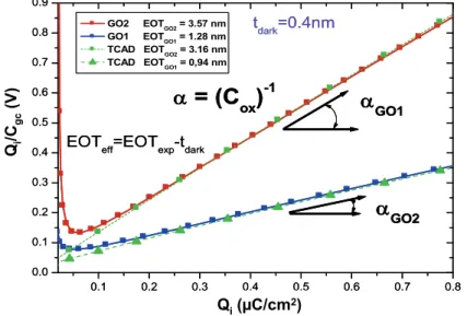
As can be seen from Eq. [1] and reported in Fig. 5, the variations of Qi/Cgc as a function of Qi well follow straight lines and by turn can be used to extract the oxide capacitance from the slope. In this case, Cox is extracted for two technological flavors, namely GO1 and GO2, of the gate oxide and therefore furnishes the corresponding EOT’s after correction of the dark space thickness [MOH 15].
0.1 0.2 0.3 0.4 0.5 0.6 0.7 0.8 0.0 0.1 0.2 0.3 0.4 0.5 0.6 0.7 0.8 0.9
EOTeff=EOTexp-tdark
tdark=0.4nm
GO2 EOTGO2 = 3.57 nm
GO1 EOTGO1 = 1.28 nm
TCAD EOTGO2 = 3.16 nm
TCAD EOTGO1 = 0,94 nm
GO2 GO1 = (Cox)-1 Q in v C gc -1 [V ] Q i n v [ µ C · c m - 2] Qi(µC/cm2) Qi /Cgc (V) 0.1 0.2 0.3 0.4 0.5 0.6 0.7 0.8 0.0 0.1 0.2 0.3 0.4 0.5 0.6 0.7 0.8 0.9
EOTeff=EOTexp-tdark
tdark=0.4nm
GO2 EOTGO2 = 3.57 nm
GO1 EOTGO1 = 1.28 nm
TCAD EOTGO2 = 3.16 nm
TCAD EOTGO1 = 0,94 nm
GO2 GO1 = (Cox)-1 Q in v C gc -1 [V ] Q i n v [ µ C · c m - 2] Qi(µC/cm2) Qi /Cgc (V)
Figure 5. Experimental (symbols) and simulated (lines) variations of Qi/Cgc vs Qi for GO1 and GO2 gate
It should also be mentioned that a better determination of the BOX thickness without any extra fitting can be conducted by directly measuring the back gate-to-channel capacitance characteristic Cbc(Vb) as exemplified in Fig. 6 [MOH 15]. For this case, it should be emphasized that both front and back gate oxide flavors GO1 and GO2 provide in a consistent way the same maximum capacitance equal to Cbox. It should also be noted that no dark space correction is necessary to obtain the buried oxide EOT since the BOX is sufficiently thick (in this case around 21nm).
-8 -6 -4 -2 0.00 0.04 0.08 0.12 0.15 S=104m2 C bc [ 10 -2 F/ m 2 ] Vb [V] GO2 GO1 Vb(V) Cbc (µ F /cm 2) Cbox -8 -6 -4 -2 0.00 0.04 0.08 0.12 0.15 S=104m2 C bc [ 10 -2 F/ m 2 ] Vb [V] GO2 GO1 Vb(V) Cbc (µ F /cm 2) -8 -6 -4 -2 0.00 0.04 0.08 0.12 0.15 S=104m2 C bc [ 10 -2 F/ m 2 ] Vb [V] GO2 GO1 Vb(V) Cbc (µ F /cm 2) Cbox
Figure 6. Experimental Cbc(Vb) characteristics variations for 2 front gate oxide flavors GO1 and GO2. After
[MOH 15].
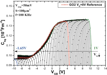
It should be mentioned that a new experimental methodology based on the exploitation of the Cbg(Vgb) characteristics has been developed [MOH 18]. An example of such characteristics is shown in Fig. 7 and enables the whole stack equivalent thickness to be extracted as well as the flat band voltage of the well (see [MOH 18] for details). It should be noted that the Cgb(Vgb) of Fig. 7 has been reconstructed after several measurements of Cgb(Vg) and Cgb(Vb) characteristics with Vb and Vg as parameters, respectively. Then, the envelope of the Cgb(Vgb) curves is exploited to obtained the flat band voltage as on a standard C-V curve [MOH 18].
-10 -8 -6 -4 -2 0 2 4 6 8 10 12 14 0.09 0.10 0.11 0.12 0.13 0.14 0.15 C bg [10 -2 Fm -2 ] VGB [V] Vstep=50mV S=100m2 f=100 KHz GO2 VG=0V Reference -1.65V 1V VG
Figure 7. Cbg versus Vgb characteristics for various Vg varying from 1V to -1.65V obtained by combining
Cgb(Vg) and Cgb(Vb) characteristics. After [MOH 18].
3. MOSFET parameter extraction
The precise extraction of MOSFET parameters is critical for better understanding the device operation and technology optimization, especially for ultra-scaled devices. Several methodologies have been developed for MOSFET parameter extraction but they are mostly restricted to the strong
inversion region and further consider that the inversion charge depends linearly on gate voltage overdrive [KRU 87, GHI 88, TAU 92, KAT 97, ORT 02, TAN 05, FLA 10]. Since the supply voltage Vdd is strongly reduced with device scaling, the strong inversion approximation is becoming less and less accurate and limits the extraction to a small gate voltage range, while losing information from around threshold to sub threshold region.
This is the reason why, new extraction procedure based on the Lambert W (LW) function, enabling the extraction of MOSFET parameters over the whole gate voltage range from 0 to Vdd, has been developed, allowing to fully take advantage of the transition from weak to strong inversion region [KAR 15]. As already mentioned in section 2, the Lambert W function is well adapted to describe the Cgc(Vg) characteristics and, by turn, the Qi(Vg) curves as shown in Fig. 8, for n channel MOS devices from a 14nm FDSOI technology. In fact, the inversion charge is well modeled by Eq. [5] [KAR 15],
nkT t V g V q ox g i V C nkTq LW e Q( ) . [5]
where n is the ideality factor controlling the subthreshold slope.
Qi (µC/cm
2)
0
0.2 0.4 0.6 0.8 1.0
V
g(V)
10
010
-210
-42
1
0
Qi
(
µC
/cm
2)
Qi (µC/cm
2)
0
0.2 0.4 0.6 0.8 1.0
V
g(V)
10
010
-210
-42
1
0
Qi
(
µC
/cm
2)
Figure 8. Experimental (solid lines) and modeled (dashed lines) Qi(Vg) characteristics of n-channel FD-SOI
MOSFETs with channel width W = 10 µm and channel length L = 3 µm. Parameters: Cox = 2.6 x 10⁻⁶ F/cm2, n
= 1.37 and Vt = 0.30 V. After [KAR 15].
In linear operation, the drain current Id of the transistor is given by:
d i eff
d WL µ QV
I [6]
where μeff is the effective mobility and Vd is the drain voltage. Moreover, using the standard degradation of the effective mobility law in strong inversion, μeff can be expressed as function of the inversion charge as:
2 2 1 0 1 i ox i ox eff C Q C Q µ µ [7]
allowing the drain current to be equated to,
2 2 1 0 1 i ox i ox d i d C Q C Q V Q µ L W I [8]
where µ0 is the low field mobility and 1, 2 are the first and second order mobility attenuation coefficients, respectively. It should be recalled that 1=10+RsdꞏGm, with Gm=(W/L)ꞏµ0ꞏCox and Rsd being the source-drain series resistance [KAR 15].
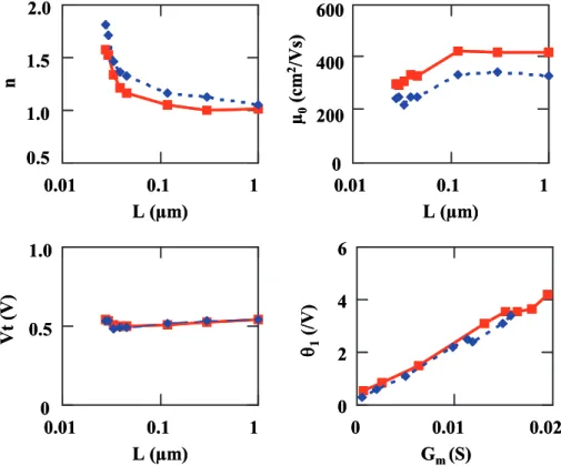
As a consequence, Eqs [5] and [8] can be employed to fit the Id(Vg) characteristics over the full gate voltage range with 5 fitting parameters, namely Vt, n, µ0, 1 and 2 (Cox being extracted separately from Cgc-Vg data as in section 2) using for example a Levenverg-Marquardt non-linear regression. This procedure has been used to fit Id(Vg) characteristics measured on nMOS devices from a 14 nm FDSOI technology and with varying gate lengths (L = 18 nm to 5 µm) as illustrated in Fig. 9. As can be seen, a very good agreement between experimental and modelled results has been achieved with a mean error of 6.5% for all gate lengths and Vg values. The major MOSFET parameters, extracted using this full gate voltage range methodology, are displayed as a function of gate length in Fig. 10. For the sake of comparison, are also reported the MOSFET parameters obtained using the Y-function method, Y(Vg)=Id/gm, which is limited to strong inversion region [GHI 88]. In all cases, the increase of short channel effect below L=30-40nm should be noted.
Id (m A ) 0.2 0.4 0.6 0.8 Vg(V) 1.0 0 0.2 0.3 0.1 0 0.4 L=18nm to 5µm Id (m A ) 0.2 0.4 0.6 0.8 Vg(V) 1.0 0 0.2 0.3 0.1 0 0.4 Id (m A ) 0.2 0.4 0.6 0.8 Vg(V) 1.0 0 0.2 0.3 0.1 0 0.4 0.2 0.4 0.6 0.8 Vg(V) 1.0 0 0.2 0.3 0.1 0 0.4 L=18nm to 5µm L=18nm to 5µm 0.2 0.4 0.6 0.8 Vg(V) 1.0 0 Id (A ) 10-12 10-8 10-6 10-4 10-10 L=18nm to 5µm 0.2 0.4 0.6 0.8 Vg(V) 1.0 0 Id (A ) 10-12 10-8 10-6 10-4 10-10 0.2 0.4 0.6 0.8 Vg(V) 1.0 0 Id (A ) 10-12 10-8 10-6 10-4 10-10 L=18nm to 5µm
Figure 9. Experimental (solid lines) and modeled (dashed lines) Id(Vg) characteristics of n-MOS FD-SOI
devices in linear (left) and logarithmic (right) scales for gate lengths L ranging from 18 nm to 5 µm and gate width W=10µm. After [KAR 15].
µ0 (cm 2/V s) 0 0.1 0.2 0.3 0.4 0 100 200 300 10-2 10-1 100 101 L (µm) Vt (V) µ0 (cm 2/V s) 0 0.1 0.2 0.3 0.4 0 100 200 300 10-2 10-1 100 101 L (µm) Vt (V) 10-2 10-1 100 101 L (µm) 1.0 1.5 2.0 Idea li ty fac to r n 10-2 10-1 100 101 L (µm) 1.0 1.5 2.0 Idea li ty fac to r n 0 0.05 0.1 -5 0 5 10 0.15 Gm (S/V) 1 (/V) Rsd 0 0.05 0.1 -5 0 5 10 0.15 Gm (S/V) 1 (/V) Rsd
Figure 10. Variation of Vt and µ0 (left), ideality factor n (middle) and first order mobility attenuation factor 1 (right) with gate length. Solid lines: parameters extracted from full gate voltage range methodology, dashed
lines: Vt and µ0 extracted using Y-function method. The ideality factor n is also directly extracted from subthreshold slope (dashed line). Gate width W=10 µm.After [KAR 15].
As is usual [GHI 88], the access resistance Rsd can be determined from the slope of the linear variation of 1 with Gm (Fig. 10). In this case, we found Rsd = 840 .µm in n-MOS devices in good agreement with the values extracted from the standard Y-function method.
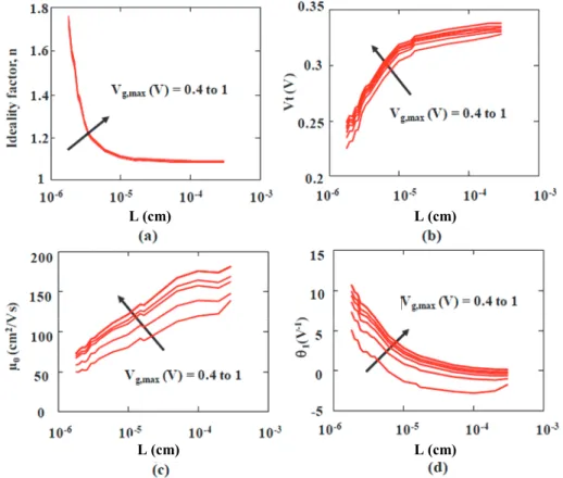
It should be underlined that the advantage of this full range parameter extraction methodology is that it can be employed with lower supply voltage. Indeed, it can be demonstrated that the MOSFET parameters can still be reliably determined down to Vg values getting close to gate voltage where the transconductance passes through a maximum, in this case, down to 0.4-0.5 V as illustrated in Fig. 11.
L (cm) L (cm)
L (cm) L (cm)
L (cm) L (cm)
L (cm) L (cm)
Figure 11. Variation of the ideality factor n (a), threshold voltage Vt (b), low-field mobility µ0 (c) and first order
attenuation factor 1 (d) with the gate length for various gate voltage ranges for nMOS FDSOI devices. After
[KAR 17].
As an alternative to the above-mentioned Lambert function method, a new Y-function based extraction methodology applicable from weak to strong inversion and not limited to above or near threshold region has been developed for MOSFET parameter extraction under low voltage operation [HEN 16]. However, contrary to Lambert W function, it cannot be also used as a compact model for the MOSFET. First, it has been shown that the inversion charge Qi(Vg) and the inversion capacitance Cgc(Vg) characteristics could be described analytically as a function of the Y-function from weak to strong inversion region. Thus, the drain current could be related to the Y-function as [HEN 16],
Y Y q kT n g I I Y m d d 1 2 1 [9]
where =Gm.Vd is the gain factor. Consequently, Eq. [9] indicates that the variation of Y2/Id (=Id/gm) with Y should follow a parabolic behaviour with coefficients providing the three MOSFET parameters n, i.e. µ0 and 1. An example of such fits is illustrated in Fig. 12 as applied to a 28nm FDSOI technology [HEN 16].
0
2
4
6
0
0.5
1
1.5
Y (A
1/2V
1/2)
Id/
gm
(/V
)
L=
1µm
28nm
0
2
4
6
0
0.5
1
1.5
Y (A
1/2V
1/2)
Id/
gm
(/V
)
L=
1µm
28nm
Figure 12. Experimental (solid lines) and modeled (symbols) Id/gm(Y) characteristics for various gate lengths
L=28nm to L=1µm (W=1µm, Cox=1.83x10⁻⁶F/cm2). Gate voltage range Vgmax= 1V. After [HEN 16].
All the MOSFET parameters (µ0, 1, n, Vt), obtained using this new Y-function based method and from the standard Y-function or subthreshold slope methods with maximum gate voltage range Vgmax=1V, are shown as a function of gate length in Fig. 13. Note the consistency of the extracted parameters vs L for µ0,n, Vt and 1. Note also that n is only extracted from new Y-function method and from subthreshold slope method.
0.01 0.1 1 0.5 1.0 1.5 2.0 L (µm) 0.01 0.1 1 0 200 400 600 L (µm) 0.01 0.1 1 0 0.5 1.0 Vt (V ) L (µm) 0 0.01 0.02 0 2 4 6 Gm(S) n µ0 (cm 2/V s) 1 (/ V ) 0.01 0.1 1 0.5 1.0 1.5 2.0 L (µm) 0.01 0.1 1 0 200 400 600 L (µm) 0.01 0.1 1 0 0.5 1.0 Vt (V ) L (µm) 0 0.01 0.02 0 2 4 6 Gm(S) n µ0 (cm 2/V s) 1 (/ V )
Figure 13. Variations of ideality factor n, µ0 and Vt with gate length and 1 with Gm as obtained from new
Y-function method (solid lines) and from standard Y-Y-function or subthreshold slope methods (dashed lines) for a
gate voltage range Vgmax=1V. Here, 100.3/V is constant with gate length.
4. Transport parameters
The carrier mobility is a key parameter determining the MOS device operation. Several techniques can be used to measure or extract the effective mobility in MOSFETs such as from Id(Vg) curves using
e.g. Y-function [GHI 88], as in section III, by split C-V method [SOD 82, ROM 04] or from magneto-transport measurements like Hall effect [NEG 11] or magneto-resistance [MEZ 04].
The low field mobility µ0 extracted from Y-function can be investigated as a function of temperature (T) and channel length in order to identify the main scattering mechanisms in the MOS device channel. Figure 14 gives an example of µ0(T) variations obtained in 14nm FDSOI nMOS devices [SHI 15a], illustrating the huge evolution of the scattering mechanisms with channel length. Indeed, in long channels, µ0 varies typically as T-1, meaning that phonon scattering dominates, whereas in short channels, µ0 is lower in amplitude and nearly independent of temperature, meaning that neutral defect scattering prevails [SHI 15a].
50 100 150 200 250 300 0 300 600 900 1200 Experiments Calculated 0 (c m 2 V -1 s -1 ) T(K) Leff= 15nm L = 10μm W = 1μm
Figure 14. Experimental (symbols) and modeled (lines) variation of low field mobility µ0 with temperature as
obtained on nMOS devices with various gate lengths. After [SHI 15a].
In order to get a quantitative picture of the scattering behaviour with temperature, the mobility can be described by the empirical model [SHI 15a]:
Tµph T µC µnd µ 1 300 1 300 1 1 0 [9]
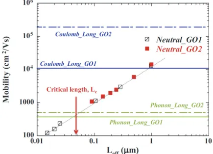
which is based on Mathiessen's rule and composed with different scattering mechanisms such as phonon, Coulomb and neutral defect scattering (μph, μC and μnd, respectively). This mobility empirical model enables a satisfactory fitting of the µ0(T) curves (Fig. 14) and, by turn, allows to extract the variations of the different scattering mechanisms with channel length for room temperature as illustrated in Fig. 15. As can be seen from this figure, both the phonon and Coulomb scattering mobility components are found to be independent of gate length, whereas the neutral scattering mobility µnd is clearly increasing with gate length. This behavior for µnd can be well interpreted by an exponential profile of process-induced neutral defects close to source-drain ends and featuring a critical distance of 10nm and a maximum concentration of about 8×1019cm-3 [SHI 15a]. Note also that the neutral mobility component is independent of the gate oxide thickness (GO1 and GO2), indicating that the neutral defects are located in the channel and not in the gate dielectric, emphasizing the consistency of the interpretation [SHI 15a].
The effective mobility can also be measured by the geometric magnetoresistance effect, which results from the modulation of the local carrier velocity by the Lorentz force. Therefore, after application of a high enough magnetic field B perpendicular to the gate, the channel resistance Rch in a large transistor (W>5-6L) is increased by the amount Rch/Rch=µMR2.B2, where µMR is the so called magnetoresistance mobility. So, µMR can be measured directly without knowing the exact channel
length and is applicable below threshold [MEZ 04]. It should also be noted that µMR is not exactly equal to µeff depending on scattering mechanism and temperature [MEZ 04].
Figure 15. Variation with channel length Leff of the various mobility scattering components (phonons,
Coulomb, neutral) for T=300K as obtained on nMOS devices with two gate oxide flavors. After [SHI 15a].
Figure 16 shows typical variations of the MR mobility as a function of the inversion charge density in the channel of nMOS FDSOI devices for various temperatures [CHA 06]. The mobility at low carrier density is dominated by unscreened Coulomb scattering, then passes through a maximum versus carrier density, around threshold, mainly controlled by phonon scattering, before to decrease at large inversion charge density due to surface roughness scattering [CHA 06].
1011 1012 40 80 120 160 200 240 T = M R Mobi lity (cm 2 V -1 s -1 ) 290 K 200 K 100 K 50 K 25 K NMOS L = 0.6 m, W = 10 m Electron Density (cm-2) Coulomb Phonons SR 1011 1012 40 80 120 160 200 240 T = M R Mobi lity (cm 2 V -1 s -1 ) 290 K 200 K 100 K 50 K 25 K NMOS L = 0.6 m, W = 10 m Electron Density (cm-2) Coulomb Phonons SR
Figure 16. Variation of MR mobility with electron density for various temperatures as obtained on nMOS
FDSOI devices. After [CHA 06].
Interestingly, the magnetoresistance effect can be measured not only in linear region but also as a function of drain voltage Vd up to saturation region as illustrated in Fig. 17 [SHI 15b]. This means that it is possible to extract the MR mobility versus drain voltage and, by turn, to plot the variation of µMR with gate voltage for various drain voltages Vd from linear to saturation region as shown in Fig. 18. It should also be noted that these MR mobility data have been very well interpreted and fitted by a semi-analytical model of drain current relying on Lambert W function. In this context, based on the gradual channel approximation, the drain current is obtained by integration along the channel of the local conductance including MR effect with an inversion charge law given by Eq. [5] and allowing to
reproduce the µMR variations with both gate and drain voltages, as shown by the dashed lines in Fig. 18 [SHI 15b]. 0.0 0.1 0.2 0.3 0.4 0.5 0.6 0.7 0.8 0 50 100 150 200 250
I
d(
A)
V
d(V)
B= 0T B= 11T GO1, L =300nm @300K Vg= 0.9V 0 20 40 60 80 100 120 140 0.00 0.02 0.04 0.06 (I d0 -I dB )/ I dB ( A. U) B2(T2) Vd=0.02V Vd=0.05V Vd=0.1V Vd=0.3V Vd=0.5V Vd=0.7V GO1, L =300nm @300K Vg= 0.9V a) b)Figure 17. a) Output characteristic Id(Vd) at strong inversion (Vg = 0.9V) for different magnetic fields B from
0T to 11T at 300 K for GO1 device (W=1μm, L=0.3μm). b) Relative drain current variation (ΔId/IdB) versus B2 from linear (Vd = 0.02V) to saturation region (Vd = 0.7V). After [SHI 15b].
Figure 18. Experimental (symbols) and modeled (dashed lines) variation of µMR with gate voltage for various
drain voltages as obtained on 14nm FDSOI nMOS devices (GO1 oxide flavor and L=30nm, W=1µm). After [SHI 15b ].
5. Mismatch or Local variability
Device variability is a serious concern for the scaling down of CMOS technologies. It is well known for many years that the threshold voltage Vt and the current gain factor local mismatch are the main sources of local variability in MOS transistors [PEL 89, CRO 02], both impacting analog and logic circuits like SRAM cells. The introduction of undoped channel technologies such as FDSOI or FinFET has significantly lowered the Vt mismatch [MAT 14, RAH 13], but it has raised new issues due to the influence of source-drain series resistance and associated variability [IOA 15, MAR 12, IOA 16].
Figure 19 shows typical set of drain current mismatch characteristics ΔId/Id(Vg) obtained on nMOS paired transistors with nominal geometry from 14nm FDSOI technology. Note the huge Id mismatch below threshold (> 2-3 decades), which requires evaluating the drain current mismatch between pairs using the log difference, Id/Idln(Id1/Id2) instead of linear difference as emphasized in [IOA 15].
‐6 ‐4 ‐2 0 2 4 6 0 0.2 0.4 0.6 0.8 ΔId /Id Vg(V) FDSOI 14nm_(W/L)=(0.06/0.02)μm 170 dies
Figure 19. Typical drain current mismatch characteristics ΔId/Id(Vg) for n-MOS paired devices from 14nm
FDSOI. After [IOA 16].
The local mismatch of the associated Y-function, ΔY/Y(Vg) are shown in Fig. 20. According to [IOA 15], this function allows removing the impact of Rsd in matching analysis.
‐4.0 ‐3.0 ‐2.0 ‐1.0 0.0 1.0 2.0 3.0 0 0.2 0.4 0.6 0.8 ΔY /Y Vg(V) FDSOI 14nm_(W/L)=(0.06/0.02)μm 170 dies
Figure 20. Typical Y-function mismatch characteristics ΔY/Y(Vg) for n-MOS paired devices from 14nm FDSOI.
After [IOA 16].
The standard deviation of the associated drain current (Id/Id) and Y function (Y/Y) mismatch vs gate voltage are shown in Fig. 21. These characteristics can be well fitted with the matching model
given in Eqs [10] and [11] and which accounts for 3 matching parameters i.e. (Vt), (/) and (Rsd) as [IOA 15], 2 sd 2 2 2 2 t 2 2 d d) . ( V) (1 . ) . ( / ) . ( R ) I I ( d sd d d m G R G I g [10] and 2 2 2 2 2 t 2 . ( β/β) 4 1 / . . . 4 ) V ( . ) Y Y ( Y q kT n [11]
where Gd is the channel conductance and =WCoxµ0Vd/L is the gain factor. According to this model, it should be noted that the Y-function variability is dominated by the Vt mismatch below threshold and then decreases to a plateau limited by the mismatch at strong inversion. This behavior is similar for the drain current variability except that there is an additional contribution of Rsd mismatch above threshold, which tends to prevail for large W/L ratios [IOA 15, IOA 16].
1.E‐03 1.E‐02 1.E‐01 1.E+00 1.E+01 0 0.2 0.4 0.6 0.8 1 σ( Δ Id /Id ) Vg(V) (W/L)=(1/0.35)μm_FDSOI 14nm (W/L)=(0.06/0.02)μm_FDSOI 14nm model (W/L)=(0.08/0.03)μm_FDSOI 28nm (W/L)=(1/0.1)μm_FDSOI 28nm 1.00E‐03 1.00E‐02 1.00E‐01 1.00E+00 0 0.2 0.4 0.6 0.8 1 σ( ΔY /Y) Vg(V) (W/L)=(10/1)μm_14nm FDSOI model (W/L)=(0.3/0.35)μm_14nm FDSOI (W/L)=(1/0.1)μm_28nm FDSOI (W/L)=(0.08/0.03)μm_28nm FDSOI
Figure 21. Experimental (symbols) and modeled (lines) σ(ΔId/Id) (left) and vs σ(ΔY/Y) (right) vs Vg curves for
n-MOS devices with various geometries from 14nm FDSOI and from 28nm FDSOI technologies. After [IOA 16].
The corresponding area normalized matching parameters defined as iAVt=(Vt).W.L and iA/=(/). ).W.L are given in Fig. 22 for various geometries and FDSOI technologies [IOA 16]. Overall, these values demonstrate that state-of-the-art variability performances are achieved for advanced FDSOI technologies.
Finally, Fig. 23 shows that the standard deviation of the series resistance mismatch σ(ΔRsd) varies typically as the reciprocal device width. As expected, the average value of Rsd is also scaling as SD/W with SD 400 .µm for 14nm FDSOI technologies. This behavior shows that the normalized series resistance local variability σ(ΔRsd)/Rsd is nearly constant, around 15% within 1.5 times variation, as a function of width for this 14nm FDSOI technology in line with 28nm results [IOA 16].
0.0 1.0 2.0 3.0 4.0 5.0
1.0E‐03 1.0E‐02 1.0E‐01 1.0E+00
iAΔV th (mV .μm ) (W.L)(μm2) 14nm FDSOI 28nm FDSOI 28nm Bulk 20nm Bulk 0.10 1.00 10.00
1.0E‐03 1.0E‐02 1.0E‐01 1.0E+00
iA(Δβ/ β)(% .μ m) (W.L)(μm2) 14nm FDSOI 28nm FDSOI 20&28nm Bulk
Figure 22. a) iAVth vs area W.L and b) iA(/) vs area W.L for 14 and 28nm FDSOI, 28 and 20 nm Bulk
technology nodes. After [IOA 16].
104 103 102 101 100 102 101 100 10-1 10-2 W (µm) Rsd (Rsd) Resistance ( ) FDSOI 14nm 104 103 102 101 100 102 101 100 10-1 10-2 W (µm) Rsd (Rsd) Resistance ( ) FDSOI 14nm
Figure 23. Variation of (Rsd) and Rsd with device width W for 14nm FDSOI. After [IOA 16].
This drain current matching characterization and modelling have been extended to all operation region of FDSOI MOS devices [KAR 17b]. In particular, the drain current mismatch model of Eq. [10] has been generalized to non linear operation region and to include subthreshold slope varaibility through ideality factor n variations [KAR 17b]:
nn I I I I R g g R g g V I g I I D th D th D D SD d m SD d m t D m D D 2 , 2 2 , 2 2 2 2 2 2 2 ln( ) exp( ) 1 2 2 1 [12]This model enabled the fits of the drain current variance both as a function of gate voltage and drain voltage up to saturation region (see Fig. 24).
Figure 24. Experimental results (symbols) and model (lines) of σ2(ΔId/Id) versus gate (a, b) and drain (c, d)
voltage. After [KAR 17b].
6. Conclusions
We have reviewed the main electrical techniques to characterize the important MOS device parameters and illustrated them by typical results obtained on advanced FDSOI technologies. First, the capacitance-voltage measurements have been employed for the vertical stack characterization of FDSOI structures with HK/MG gate, ultra thin film channel, thin box oxide and back plane substrate. Then, the MOSFET parameter extraction methods have been illustrated, as well as the transport and mobility assessment using various techniques (I-V, magneto-transport). Finally, the methodology to study the local variability of the MOSFET electrical characteristics has been discussed.
References
[[BEN 13] I. Ben Akkez, A. Cros, C.Fenouillet-Beranger, F. Boeuf, Q. Rafhay, F. Balestra, G. Ghibaudo, “New parameter extraction method based on split C-V measurements in FDSOI MOSFETs”, Solid State Electronics, vol. 84, 142 (2013).
[CHA 06] W. Chaisantikulwat, M. Mouis, G. Ghibaudo, C. Gallon, C. Fenouillet-Beranger, D.K. Maude, T. Skotnicki, S. Cristoloveanu, “Differential Magnetoresistance Technique for Mobility Extraction in Ultra-Short Channel FDSOI Transistors”, Solid State Elecronics, vol. 50, 637 (2006).
[CRO 02] J. Croon, M. Rosmeulen, S. Decoutere, W. Sansen, H. Maes, “An easy-to-use mismatch model for the MOS transistor”, IEEE Journal of Solid-State Circuits, vol. 37, 1056 (2002).
[FEN 07] C. Fenouillet-Beranger et al, “Fully-depleted SOI technology using high-k and single-metal gate for 32 nm node LSTP applications featuring 0.179 μm2 6T-SRAM bitcell”, Proc. IEDM 2007, p. 267.
[FLA 10] D. Flandre, V. Kilchytska, and T. Rudenko, “gm/Id method for threshold voltage extraction applicable in advanced MOSFETs with nonlinear behavior above threshold,” IEEE Electron Device Lett., vol. 31, 930 (2010). [GHI 88] G. Ghibaudo, “New method for the extraction of MOSFET parameters“, IEE Electronic Letters, vol. 24, 543
(1988).
[GHI 00] G. Ghibaudo, S. Bruyère, T. Devoivre, B. DeSalvo, and E. Vincent, “Improved method for the oxide thickness extraction in MOS structures with ultra thin gate dielectrics”, IEEE Transaction on Semiconductor Manufacturing, vol. 13, 152 (2000).
[HEN 16] J.B. Henry, Q. Rafhay, A. Cros, and G. Ghibaudo, “New Y-function based MOSFET parameter extraction method from weak to strong inversion range”, Solid State Electron., vol. 123, 84 (2016).
[IOA 15] E. G. Ioannidis, C. G. Theodorou, S. Haendler, E. Josse, C. A. Dimitriadis, G. Ghibaudo, “Impact of source-drain series resistance on source-drain current mismatch in advanced Fully Depleted SOI n-MOSFETs”, IEEE Electron Device Letters, vol. 36, 433 (2015).
[IOA 16] E. G. Ioannidis et al, “Characterization and modeling of drain current local variability in 28 and 14 nm FDSOI nMOSFETs”, Solid State Electron., vol. 118, 4 (2016).
[KAR 15] T. A. Karatsori, C. G. Theodorou, E. G. Ioannidis, S. Haendler, E. Josse, C. A. Dimitriadis and G. Ghibaudo, “Full gate voltage range Lambert-function based methodology for FDSOI MOSFET parameter extraction”, Solid State Electronics, vol. 111, 123 (2015).
[KAR 17a] T. Karatsori, “Electrical Characterization and Modeling of Advanced Nano-scale Ultra Thin Body and Buried Oxide MOSFETs and Application in Circuit Simulations”, PhD thesis, University Grenoble Alpes (2017).
[KAR 17b] T. A. Karatsori, C. G. Theodorou, E. Josse, C. A. Dimitriadis, , and G. Ghibaudo, “All operation region characterization and modeling of drain and gate current mismatch in 14nm Fully Depleted SOI MOSFETs”, IEEE Trans Electron Devices, vol. 64, 2080 (2017).
[KAT 97] H. Katto, “Device parameter extraction in the linear region of MOSFET’s,” IEEE Trans. Electron Devices, vol. 18, 408 (1997).
[KRU 87] T. J. Krutsick, M. H. White, H.-S. Wong, and R. V. Booth, “An improved model of MOSFET modeling and parameter extraction,” IEEE Trans. Electron Devices, vol. 34, 1676 (1987).
[MAR 12] S. Markov, Cheng Binjie, A. Asenov, “Statistical Variability in Fully Depleted SOI MOSFETs Due to Random Dopant Fluctuations in the Source and Drain Extensions”, IEEE Electron Device Letters, vol. 33, 315 (2012). MAS 74] J. Maserjian, G. Petersen, and C. Svensson, “Saturation capacitance of thin oxide MOS structures and the
effective surface density of states of silicon,” Solid State Electron., vol. 17, 335 (1974).
[MAT 14] T. Matsukawa, K. Fukuda, Y.X. Liu, K. Endo, J. Tsukada, H. Yamauchi, Y. Ishikawa, S. O'uchi, W. Mizubayashi, S. Migita, Y. Morita, H. Ota, M. Masahara, “Lowest variability SOI FinFETs having multiple Vt by back-biasing”, Symposium on VLSI Technology, 2014, p. 1.
[MEZ 04] Y. M. Meziani, J. Łusakowski, W. Knap, N.Dyakonova, F.Teppe , K. Romanjek, M. Ferrier, R. Clerc, G. Ghibaudo, F. Boeuf and T. Skotnicki, “Magnetoresistance characterization of nanometer Si metal-oxide-semiconductor transistors”, Journal Applied Physics, vol. 96, 5761 (2004).
[MOH 15] B. Mohamad, G. Ghibaudo, C. Leroux, E. Josse, G. Reimbold, “Full Front and Back Split C-V characterization of CMOS devices from 14nm node FDSOI technology”, Proc. IEEE S3S Conference, 2015, p. 1. [MOH 18] B. Mohamad, C. Leroux, G. Reimbold, G. Ghibaudo, “Determination of well flat band condition in thin film
FDSOI transistors using C-V measurement for accurate parameter extraction”, Solid State Electronics, vol. 139, 88 (2018).
[NAV 15] C. Navarro, M. Bawedin, , F. Andrieu, J. Cluzel, S. Cristoloveanu, “Fully Depleted SOI Characterization by Capacitance Analysis of p-i-n Gated Diodes”, IEEE Electron Device Letters, vol. 36, 5 (2015).
[NEG 11] M. A. Negara, D. Veksler, J. Huang, G. Ghibaudo, P.K. Hurley, G. Bersuker, N. Goel, and P. Kirsch, “Analysis of Effective Mobility and Hall Effect Mobility in High-k based In0.75Ga0.25As metal-oxide-semiconductor high-electron-mobility transistors”, Applied Physics Letters, vol. 99, 232101 (2011).
[ORT 02] A. Ortiz-Conde, F. J. Garcia Sanchez, J. J. Liou, A. Cerdeira, M. Estrada, and Y. Yue, “A review of recent MOSFET threshold voltage extraction methods,” Microelectron. Reliab., vol. 42, 583 (2002).
[PEL 89] M. J. M. Pelgrom, Aad C. J. Duinmaijer and Anton P. G. Welbers, “Matching Properties of MOS transistors”, IEEE Journal of Solid-State Circuits, vol. 24, 1433 (1989).
[RAH 13] L. Rahhal, A. Bajolet, C. Diouf, A. Cros, J. Rosa, N. Planes, G. Ghibaudo, “New methodology for drain current local variability characterization using Y function method”, IEEE International Conference on Microelectronic Test Structures (ICMTS), 2013 , p. 99.
[ROM 04] K. Romanjek, F. Andrieu, T. Ernst, and G. Ghibaudo, “Improved split C(V) method for effective mobility extraction in sub 0.1 µm Si MOSFETs”, IEEE Electron Device Letters, vol. 25, 583 (2004).
[SHI 14] M. Shin, M. Shi, M. Mouis, A. Cros, E. Josse, G.-T. Kim and G. Ghibaudo, “Full split C-V method for parameter extraction in Ultra Thin BOX FDSOI MOS devices”, Solid State Electronics, vol. 99, 104 (2014).
[SHI 15a] M. Shin, M. Shi, M. Mouis, A. Cros, E. Josse, S. Mukhopadhyay, B. Piot, G.-T. Kim and G. Ghibaudo, “In depth characterization of electron transport in 14nm FD-SOI CMOS devices”, Solid State Electronics, vol. 112, 13 ( 2015).
[SHI 15b] M. Shin, M. Shi, M. Mouis, A. Cros, E. Josse, S. Mukhopadhyay, B. Piot, G.-T. Kim and G. Ghibaudo, “Experimental and theoretical investigation of magnetoresistance from linear regime to saturation in 14nm FDSOI MOS devices”, IEEE Trans Electron Devices, vol. 62,. 3 (2015).
[SOD 82] C. Sodini, T. Ekstedt, J. Moll, “Charge accumulation and mobility in thin dielectric MOS transistors”, Sol. State Electron., vol 25, 833 (1982).
[SUG 08] N. Sugii et al, “Comprehensive study on Vth variability in silicon on Thin BOX (SOTB) CMOS with small random-dopant fluctuation: Finding a way to further reduce variation”, Proc. IEDM 2008, p. 249.
[TAN 05] T. Tanaka, “Novel extraction method for size-dependent mobility based on BSIM3-like compact model, “Japanese Journal of Applied Physics, vol. 44, 2424 (2005).
[TAU 92] T. Taur, D. S. Zicherman, D. R. Lombardi, P. J. Restle, C. H. Hsu, H. I. Nanafi, M. R. Wordeman, B. Davari, and G. G. Shahidi, “A new ‘shift and ratio’ method for MOSFET channel-length extraction,” IEEE Electron Device Lett., vol. 13, pp. 267-269, 1992.
[WEB 08] O. Weber et al, “High immunity to threshold voltage variability in undoped ultra-thin FDSOI MOSFETs and its physical understanding”, Proc. IEDM 2008, p. 245.


![Figure 14 gives an example of µ 0 (T) variations obtained in 14nm FDSOI nMOS devices [SHI 15a], illustrating the huge evolution of the scattering mechanisms with channel length](https://thumb-eu.123doks.com/thumbv2/123doknet/15034234.689364/10.892.259.650.259.539/figure-example-variations-obtained-illustrating-evolution-scattering-mechanisms.webp)