HAL Id: hal-03012129
https://hal.laas.fr/hal-03012129
Submitted on 18 Nov 2020
HAL is a multi-disciplinary open access
archive for the deposit and dissemination of
sci-entific research documents, whether they are
pub-lished or not. The documents may come from
teaching and research institutions in France or
abroad, or from public or private research centers.
L’archive ouverte pluridisciplinaire HAL, est
destinée au dépôt et à la diffusion de documents
scientifiques de niveau recherche, publiés ou non,
émanant des établissements d’enseignement et de
recherche français ou étrangers, des laboratoires
publics ou privés.
Development of 1 eV InGaAsN PIN subcell for MJSC
integration and space application
Maxime Levillayer, Sophie Duzellier, Hélène Carrère, Inès Massiot, Thierry
Nuns, Stéphanie Parola, Alexandre Arnoult, Christophe Inguimbert, Laurent
Artola, Chantal Fontaine, et al.
To cite this version:
Maxime Levillayer, Sophie Duzellier, Hélène Carrère, Inès Massiot, Thierry Nuns, et al..
De-velopment of 1 eV InGaAsN PIN subcell for MJSC integration and space application.
47th
IEEE Photovoltaic Specialists Conference (PVSC 47), IEEE, Jun 2020, Calgary (virtual), Canada.
�10.1109/PVSC45281.2020.9300570�. �hal-03012129�
Development of 1 eV InGaAsN PIN subcell for
MJSC integration and space application
Maxime Levillayer
ONERA/DPHY, Univ of Toulouse
Toulouse, France [email protected]
Sophie Duzellier
ONERA/DPHY, Univ of Toulouse
Toulouse, France [email protected] Hélène Carrère LPCNO, INSA-UPS-CNRS Toulouse, France [email protected] Inès Massiot LAAS-CNRS Toulouse, France [email protected] Thierry Nuns
ONERA/DPHY, Univ of Toulouse
Toulouse, France [email protected]
Stéphanie Parola
IES, Univ of Montpellier, CNRS
Montpellier, France [email protected] Alexandre Arnoult LAAS-CNRS Toulouse, France [email protected] Christophe Inguimbert
ONERA/DPHY, Univ of Toulouse
Toulouse, France [email protected]
Laurent Artola
ONERA/DPHY, Univ of Toulouse
Toulouse, France [email protected] Chantal Fontaine LAAS-CNRS Toulouse, France [email protected] Corinne Aicardi CNES Toulouse, France [email protected] Guilhem Almuneau LAAS-CNRS Toulouse, France [email protected]
Abstract—This paper reports on the optimization of 1eV
dilute nitride solar cells growth conditions. InGaAsN cells were grown by MBE under different conditions (V/III ratio, substrate temperature, surfactant) and were processed without post-growth annealing. Characterization results suggest that the V/III ratio should be kept above 10 and that using Bi as a surfactant does not improve the cell performances. Our best InGaAsN cells exhibit Jsc and Voc values of 7.9 mA/cm2 and 0.375 V respectively,
under AM0> 870 nm and without ARC.
Keywords—InGaAsN, 1eV cell, MJSC, dilute nitride, space applications
I. INTRODUCTION
Multijunction solar cells (MJSC) based on III-V semiconductors offer today the highest photovoltaic efficiencies as illustrated by the 47.1% record held by a 6-junctions cell under concentration [1]. Consequently, those cells are of prime interest for energy harvesting in space systems where W/kg is the key parameter. However, most efficient MJSC remain at laboratory scale and require complex mechanical processing steps such as substrate report or wafer bonding. These steps are difficult to implement at the industrial scale, which explains the current interest for monolithic growth. Indeed, today’s market for high performance MJSC for space is dominated by GaInP/(In)GaAs/Ge trijunction cells lattice-matched to their substrate, with 28-30% efficiency.
Theoretical calculations of the optimal bandgap combination pointed out the need to develop a 1eV subcell to improve spectral overlapping [2]. This subcell could replace Ge as the bottom cell in the current state-of-the-art trijunction or be integrated within a 4-junctions to tackle the theoretical efficiency limit of 38 and 41%, respectively. Dilute nitrides have been studied as potential candidates for this application as nitrogen induces a high bandgap bowing coefficient for small N concentration [3]. Tuning In and N composition in the InGaAsN quaternary allows then to lower the bandgap while remaining lattice-matched to GaAs or Ge substrates.
However, the growth of dilute nitride semiconductors was proven to be difficult because of the small size and the high electronegativity of the nitrogen anion leading to the formation of N induced defects detrimental to the cell properties [4,5,6]. For molecular beam epitaxy (MBE), a study pointed out the necessity of growing InGaAsN within a 420-480°C temperature window to ensure a high quality two-dimensional growth [7]. The other important growth parameter is the ratio between elements V and III approximated here as the As/III beam equivalent pressure (BEP) ratio. Indeed, As overpressure is reported to have a strong impact on the optical and electrical properties of InGaAsN as it affects the N incorporation rate and the N nearest-neighbour configuration [6,8].
Regarding 1eV subcells, today’s main challenge is to reach short circuit current density (Jsc) values large enough to satisfy
the current matching condition within the MJSC. Jsc higher
than 15 mA/cm2 have been reported for AM0> 870 nm [6] and
AM1.5> 830 nm [9] irradiance but both results were achieved with bandgap lower than 1eV (0.93 and 0.9eV respectively) and FF values were not reported.
Optimization studies were already conducted by varying one growth parameter (T or V/III) while keeping the other parameters fixed [6, 7]. However, we can reasonably assume that the optimum couple (T;V/III) depends on the targeted nitrogen concentration and remains yet to be found for a 1eV dilute nitride. Furthermore, the optimization is usually carried out by considering the properties of the cell after annealing, which can be a complicated step to implement during the MJSC monolithic growth.
Our approach consists then in optimizing the MBE growth of 1eV InGaAsN alloys that does not require a post-growth rapid thermal processing (RTP). In order to identify the best growth parameters, InGaAsN cells were characterized with various techniques such as external quantum efficiency (EQE), photoluminescence (PL) and I(V) under dark and AM0 illumination conditions.
II. EXPERIMENTAL METHOD
InGaAsN p-i-n cells were grown by MBE at LAAS-CNRS on 4-inch n-GaAs (001) substrates in a Riber 412 system equipped with a RF valved plasma nitrogen source. The devices consist in a p-i-n GaAs/InGaAsN/GaAs structure including a n-Al0.4Ga0.6As back surface field (BSF), a
p-Al0.4Ga0.6As front surface field (FSF) and a p+ GaAs cap layer
(Fig. 1a). InGaAsN growth conditions were changed from one sample to the other (see Table 1) while identical conditions were used for the rest of the structure. In composition was calibrated based on the PL signal of InGaAs quantum wells. Nitrogen composition was controlled through a homemade in-situ curvature measurement setup [10] allowing us to tune the N flow into the growth reactor in order to preserve an adequate In/N ratio and remain lattice-matched to GaAs. The composition of the InGaAsN active layer was set to 6.5% for In and ≈ 2.2% N corresponding to the lattice-matched condition.
AuGeNiAu metallization was carried out on the backside by sputtering and TiAu contacts were deposited on the frontside by e-beam evaporation through patterning photolithography and lift-off steps. Wafers were then annealed at 350°C during 90 s in order to achieve good ohmic contacts. Mesa wet etching was performed using H3PO4/H2O2 and the
GaAs cap layer was selectively removed using C6H8O7/H2O2.
No anti-reflective coating (ARC) was deposited. Wafers were finally cleaved in 0.25cm2 and 1cm2 cells with grid densities
ranging from 0 to 10%. The processed cell structure cutview is shown in Fig. 1b.
TABLE I. INGAASN GROWTH CONDITIONS
Sample Surfactant Growth Temperature As/III ratio
A Bi 480°C 12
B Ø 480°C 12
C Ø 460°C 10
D Ø 500°C 10
Fig. 1. Structure of the cell after epitaxy (a) and after processing steps (b)
III. RESULTS AND DISCUSSION A. Effect of the growth conditions
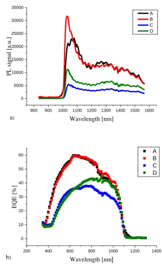
Photoluminescence measurements were performed at 10K on as-grown wafers using a Ti-Sa pulsed 950 nm laser excitation source. Results are shown in Fig. 2a). In addition, we have conducted EQE measurements on solar cells processed from those wafers, as reported in Fig. 2b).
The PL and EQE results show a strong correlation enabling to estimate the InGaAsN bandgap at 1.12eV. Comparing samples A and B, we can see that bismuth used as a surfactant does not improve optical properties. Moreover, slightly larger dark current densities are observed with devices grown with Bi.
Both PL and EQE point out that cells grown with a ratio As/III =12 exhibit better optical properties than those grown with a ratio equal to 10. This difference is likely due to an increase in the density of non-radiative recombination centers in the active layer. The rather large drop in quantum efficiency for lower As/III ratio could originate from degraded carrier collection in the absorbing layer. Indeed, those p-i-n cells rely on a field aided collection regime which can only be guaranteed if the background carrier concentration (BGCC) is low enough in the pseudo-intrinsic layer.
Fig. 2. a) PL spectra of InGaAsN cells, b) EQE of InGaAsN cells
800 900 1000 1100 1200 1300 1400 1500 1600 0 5000 10000 15000 20000 25000 30000 35000 A B C D PL si gnal [a. u.] Wavelength [nm] a) 200 400 600 800 1000 1200 1400 0 10 20 30 40 50 60 A B C D EQ E [%] Wavelength [nm] b)
Relatively high doping concentration can prevent the space charge region to extend within the whole active layer resulting in lower collection efficiency as it was studied in [11]. Reference [12] also reports that under their growth conditions, 900 nm thick absorber cells are fully depleted whereas 1200 nm thick ones are not.
Reducing the As/III ratio is then supposed to promote the formation of defects acting as dopants in the InGaAsN layer. On-going C(V) investigations will provide more details about the BGCC and deep-level transient spectroscopy will be conducted to reveal the electronic nature of the defects.
B. Motivation for processing as-grown cells
RTP at 700°C and 750°C were conducted during 30 seconds on A and B samples. In contrast to a large part of literature reports [7,13,14], we found that RTP does not improve material properties. No change in dark current density was observed and PL signal was found to be higher for unannealed samples. Additionally, the characteristic InGaAsN blueshift usually seen after RTP was not observed in our case suggesting the good homogeneity of the as-grown dilute nitride layer (no N and In rich phases). Moreover, the evolution of the PL signal with temperature does not show an s-shape for the bandgap energy, implying that the exciton localization is not significant. An hypothesis for this positive result is that defect curing may occur during the growth of the GaAs/AlGaAs/GaAs top layers. Indeed, those layers were grown at 600°C, which has already been reported to be a high-enough temperature to induce self-annealing [15].
C. I(V) characteristics of the cells
I(V) measurements were performed under AM0> 870 nm illumination to evaluate the characteristics of the InGaAsN subcell in operating conditions (integrated in a MJSC). Results show that the I(V) curves confirm the results obtained from PL and EQE measurements. The highest values for Jsc, Voc and FF
were measured for samples A and B grown with the highest As/III ratio. No clear conclusions could be drawn regarding the effect of the growth temperature and this point is currently under investigation.
The best I(V) characteristics are obtained for the cells grown with a ratio As/III=12 and without Bi (sample B). We report a Jsc and a Voc equal to 7.94 mA/cm2 and 0.375 V,
respectively, under filtered AM0 illumination and without ARC. Accounting for a reflectance both simulated and measured around 30% in the 870-1300 nm spectral range, and considering no internal reflection within the MJSC, those cells would exhibit Jsc ≈ 11.4 mA/cm2 in operating conditions. To
our knowledge, this constitutes the highest PV performances ever reported for unannealed dilute nitride cells.
IV. CONCLUSIONS AND PERSPECTIVES
We have demonstrated 1.12 eV unannealed InGaAsN cells able to generate ≈ 8 mA/cm² under AM0> 870 nm without ARC. Using Bi as a surfactant and performing a RTP after growth were found not to be useful and even detrimental to some electrical and optical properties. Most importantly, it appears that the As/III ratio has to be kept higher than 10
during InGaAsN MBE growth to ensure a good material quality. Further optimizations have to be carried out and (In;N) content has to be increased to further lower the InGaAsN bandgap towards 1eV. Short-circuit density higher than 15 mA/cm2 will be required to satisfy the current matching
condition in MJSC. Finally, InGaAsN subcell integration within a MJSC needs to be demonstrated to ensure its compatibility with the rest of the structure.
ACKNOWLEDGMENT
We acknowledge the technical support from the LAAS-CNRS micro and nanotechnologies platform, a member of the French RENATECH network. The authors acknowledge F. Pichot from CTM University of Montpellier for the AuGeNiAu metallization.
REFERENCES
[1] J.F. Geisz, M.A. Steiner, N. Jain et al. “Building a six-junction inverted metamorphic concentrator solar cell,” IEEE J. Photovolt. vol. 8, pp. 626-632, 2018
[2] S.R. Kurtz, D. Myers, J.M. Olson “Projected performance of three- and four-junction devices using GaAs and GaInP,” Proceedings of the 26th
IEEE PVSC, p. 875, 1997
[3] M. Weyers, M. Sato, H. Ando “Red shift of photoluminescence and absorption in dilute GaAsN alloy layers,” Jpn. J. Appl. Phys. vol. 31, pp. 853-855, 1992
[4] R. Kaplar, D. Kwon, S.A. Ringel et al. “Deep levels in p- and n-type InGaAsN for high-efficiency multi-junction III-V solar cells,” Sol.
Energy Mater. Sol. Cells vol. 69, pp. 85–91, 2001
[5] A. Khan, S.R. Kurtz, S. Prasad, S.W. Johnston, J. Gou “Correlation of nitrogen related traps in InGaAsN with solar cell properties,” Appl.
Phys. Lett. vol. 90, 2007
[6] V. Polojarvi, A. Aho, A. Tukiainen et al. “Influence of As/group-III flux ratio on defects formation and photovoltaic performance of GaInNAs solar cells,” Sol. Energy Mater. Sol. Cells vol. 149, pp. 213–220, 2016 [7] A. Aho, V. Polojarvi, V.M. Korpijarvi et al. “Composition dependent
growth dynamics in molecular beam epitaxy of GaInNAs solar cells,”
Sol. Energy Mater. Sol. Cells vol. 124, pp. 150–158, 2014
[8] E.M. Pavalescu, T. Hakkarainen, V.D.S Dhaka et al. “Influence of arsenic pressure on photoluminescence and structural properties of GaInNAs/GaAs quantum wells grown by molecular beam epitaxy” J.
Cryst. Growth vol. 281, pp. 249-254, 2005
[9] M.M. Wilkins, J. Gupta, A. Jaouad et al. “Design of thin InGaAsN(Sb) n-i-p junctions for use in four-junction concentrating photovoltaic devices” J. Photonics Energy vol. 7(2), 2017
[10] A. Arnoult and J. Colin, Patent FR1754616, May 2017.
[11] N. Miyashita, N. Ahsan, Y. Okada “Generation and collection of photocarriers in dilute GaInNAsSb solar cells” Prog. Photovolt: Res.
Appl. vol. 24, pp. 28-37, 2016
[12] A.I. Baranov, A.S. Gudovskikh, D.A. Kudryashov et al. “Defect properties of InGaAsN layers grown as sub-monolayer digital alloys by molecular beam epitaxy” J. Appl. Phys. vol. 123, 2018
[13] K. Volz, D. Lackner, I. Nemeth et al. “Optimization of annealing conditions of (GaIn)(NAs) for solar cell applications” J. Cryst. Growth vol. 310, pp. 2222–2228, 2008.
[14] N. Miyashita, Y. He, N. Ahsan, Y. Okada “Anneal mediated deep-level dynamics in GaInNAsSb dilute nitrides lattice-matched to GaAs” J.
Appl. Phys. vol. 126, 2019
[15] E. Pavalescu, T. Jouhti, M. Dimitrescu et al. “Growth-temperature-dependent (self-)annealing-induced blueshift of photoluminescence from 1.3 µm GaInNAs/GaAs quantum wells” Appl. Phys. Lett. vol. 83(8), 2003