Publisher’s version / Version de l'éditeur:
Applied Physics Letters, 89, 11, pp. 113103-1-113103-3, 2006-07-26
READ THESE TERMS AND CONDITIONS CAREFULLY BEFORE USING THIS WEBSITE. https://nrc-publications.canada.ca/eng/copyright
Vous avez des questions? Nous pouvons vous aider. Pour communiquer directement avec un auteur, consultez la
première page de la revue dans laquelle son article a été publié afin de trouver ses coordonnées. Si vous n’arrivez pas à les repérer, communiquez avec nous à [email protected].
Questions? Contact the NRC Publications Archive team at
[email protected]. If you wish to email the authors directly, please see the first page of the publication for their contact information.
NRC Publications Archive
Archives des publications du CNRC
This publication could be one of several versions: author’s original, accepted manuscript or the publisher’s version. / La version de cette publication peut être l’une des suivantes : la version prépublication de l’auteur, la version acceptée du manuscrit ou la version de l’éditeur.
For the publisher’s version, please access the DOI link below./ Pour consulter la version de l’éditeur, utilisez le lien DOI ci-dessous.
https://doi.org/10.1063/1.2347693
Access and use of this website and the material on it are subject to the Terms and Conditions set forth at
Fast three-dimensional nanostructure fabrication by laser-assisted
nanotransfer printing
Le Drogoff, B.; Cui, B.; Veres, T.
https://publications-cnrc.canada.ca/fra/droits
L’accès à ce site Web et l’utilisation de son contenu sont assujettis aux conditions présentées dans le site LISEZ CES CONDITIONS ATTENTIVEMENT AVANT D’UTILISER CE SITE WEB.
NRC Publications Record / Notice d'Archives des publications de CNRC:
https://nrc-publications.canada.ca/eng/view/object/?id=4188600e-2166-4248-825c-bc993f3f0e92 https://publications-cnrc.canada.ca/fra/voir/objet/?id=4188600e-2166-4248-825c-bc993f3f0e92Fast three-dimensional nanostructure fabrication by laser-assisted
nanotransfer printing
B. Le Drogoff,a兲B. Cui, and T. Veres
Institut des Matériaux Industriels, Conseil National de Recherches du Canada (CNRC), Boucherville, Québec J4B 6Y4, Canada
共Received 25 January 2006; accepted 27 July 2006; published online 11 September 2006兲 The authors present a laser-assisted nanotransfer printing technique for transferring metal nanopatterns onto prepatterned substrates. A fused quartz mold covered with an array of chromium nanodots is pressed against the surface of a photolithographically patterned substrate, while a single laser pulse from a quadrupled-frequency solid state Nd:YAG laser is used to melt the thin metal structures. By controlling the laser fluence, selective metal pattern transfer can be realized only on the protruded area of the substrate upon separation of the quartz support. The transferred chromium nanodots are then used as an etch mask to pattern three-dimensional structures. © 2006 American
Institute of Physics. 关DOI:10.1063/1.2347693兴
Three-dimensional structures having nanoscale features are commonly fabricated by multiple lithography steps 关typi-cally involving photolithography and/or e-beam lithography 共EBL兲兴 with alignment or by a single lithography step with multilayer resist stacks. However, besides the low throughput of EBL, performing lithography over topography generated by the previous patterning steps presents many challenges. Among these, the resist thickness may not be uniform across a prepatterned substrate, making critical dimension control difficult, or the coverage of resist may not be conformal with voids near the edge of the previous pattern, which impedes subsequent pattern transfer by etching.
In this letter, we describe a simple laser-based process for fast printing of metal nanofeatures over prepatterned sub-strates, named laser-assisted nanotransfer printing 共LA-nTP兲. The transferred metal nanofeatures are then used as an etch mask to pattern three-dimensional 共3D兲 structures. LA-nTP is a dry-contact printing process which combines into one single step several steps needed for metal nanopatterning, such as lithography 关EBL or nanoimprint lithography 共NIL兲兴, metal deposition, and lift-off processes. This process shares some attributes with laser-induced forward transfer 共LIFT兲 process.1 In LIFT, a thin laser-light absorbing film is irradi-ated with a focused laser pulse through a transparent support, and transferred, in the form of micron-sized dots, onto a suitable substrate facing it. The pattern is created through selective deposition on the substrate by scanning the laser beam. The resolution is hence determined and limited by the laser beam size and by the gap between the two samples 共which determines the lateral spreading兲. In the LA-nTP pro-cess, we use a prepatterned transparent support in close con-tact with a substrate; therefore the resolution is no longer limited by the processing parameters but is determined only by the initial feature size on the transparent support.
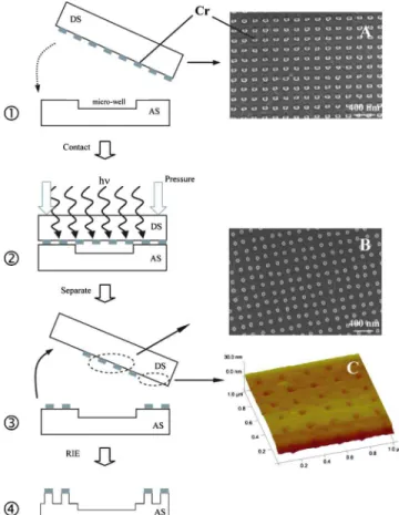
A schematic sequence of LA-nTP leading to the fabrica-tion of 3D nanoscale features is shown in Fig. 1. The first step is the generation on a substrate 共transparent to the laser irradiation兲 of the metal nanopattern to be transferred. In our case, a square chromium nanodot array 关⬃80⫻ 80 nm2,
200 nm period, and 35 nm thick 共see inset A in Fig. 1兲兴 was fabricated on an UV-grade fused quartz substrate using double NIL at orthogonal angle and lift-off. In parallel, we defined, by photolithography and reactive ion etching, the desired pattern into a 500 nm thick thermal SiO2layer. Here,
for the proof of concept, we have arbitrarily chosen an array of microwells with a diameter of 100m, 40 nm deep, and separated from each other by 100m 共edge to edge兲. The two patterned surfaces were then brought into close contact by sandwiching them between two press plates. The top plate
a兲
Author to whom correspondence should be addressed; electronic mail: [email protected]
FIG. 1. 共Color online兲 Schematic sequence of the fabrication process of 3D nanostructures by LA-nTP 共DS: donor support, AS: acceptor substrate兲. The inset pictures show the Cr nanodot pattern on the DS before 共inset A兲 and after 共inset B兲 LA-nTP. The inset C is an AFM image of the quartz support after LA-nTP.
APPLIED PHYSICS LETTERS 89, 113103 共2006兲
0003-6951/2006/89共11兲/113103/3/$23.00 89, 113103-1 © 2006 American Institute of Physics Downloaded 18 Aug 2010 to 132.246.232.2. Redistribution subject to AIP license or copyright; see http://apl.aip.org/about/rights_and_permissions
has an opening to let the laser beam through. The silicon wafer 共the acceptor substrate兲 was placed on the lower plate with the quartz donor support on top of it. Pressure was provided by a set of springs and was estimated from the constant of the springs to be about 0.69 MPa. The transfer printing process was realized when a single pulse from a quadrupled-frequency neodymium-doped yttrium aluminum garnet laser 共 = 266 nm兲 impinged the quartz support with the chromium nanopattern from the back side. The incident Gaussian laser pulse was spatially shaped using a 5 mm dia-phragm and focused to a diameter of 1 mm. At a typical laser fluence of 350 mJ/ cm2, the Cr nanodots are transferred only onto the protruded parts of the acceptor substrate that are in intimate contact with the donor support.
Figure 2 shows the result of the transferred nanopattern after LA-nTP. It can be seen that the transfer follows the topography of the prepatterned acceptor substrate with an excellent control over a large scale. The protruding area around the microwell was totally covered with Cr nanodots, while none was found on the recessed area 共which is only 40 nm deep兲. A close look at the transferred nanodots 共inset of Fig. 2兲 and the ones remaining on the donor support 共inset B of Fig. 1兲 reveals that LA-nTP heats Cr nanodots into a molten state, changing the initially square Cr dots into rounded dot ones due to the very high metal surface tension. The transferred and the nontransferred nanodots have a mean diameter of 95 and 80 nm, respectively, both with the same periodicity as the original pattern. This slight increase 共⬃20% 兲 of the transferred nanodots diameter during the printing transfer can be explained by the applied pressure that squeezed the melted Cr. Atomic force microscope 共AFM兲 measurements also reveal that the height of the trans-ferred nanodots is ⬃45 nm. The difference with the initial thickness of the Cr nanodots 共⬃35 nm兲 might be due to the transfer of some melted silica on top of the Cr nanodots. Indeed, as illustrated in inset C of Fig. 1, we can clearly see in this AFM image the presence of tiny holes 共5 – 10 nm deep兲 on the surface of the quartz plate after LA-nTP, with the same periodicity as the Cr nanodot array that was on the surface before. 关It is worth mentioning that direct irradiation of the bare SiO2substrate at the same fluence did not lead to
any melting damage due to the much larger optical
penetra-tion depth of SiO2 共␣−1⬎1 cm at 0.25m兲. 2
It was also verified that the formation of these holes is not due to the fabrication process of the Cr nanodots array.兴 We also found that using higher fluences 共⬎600 mJ/ cm2兲, the results ob-tained were similar to those observed in other LIFT studies,1 i.e., Cr material was transferred on the protruded areas as well as on the recessed areas of the acceptor substrate with an increasing amount of spatter. At even higher fluences 共⬎1 J / cm2兲, significant chromium vaporization was
ob-served. On the other hand, experiments using laser fluences lower than ⬃200 mJ/ cm2 共i.e., below the melting threshold of a 30 nm Cr thin film3兲 failed to transfer the Cr nanopat-terns. Finally, the transferred Cr nanodots were used as an etch mask to complete 3D structure fabrication. Figure 3 shows the 100 nm high nanopillars on the protruded area of a microwell obtained after etching into SiO2.
In order to understand the underlying physics in the LA-nTP process, a simple two-dimensional numerical model was developed to solve the heat conduction equation using COMSOLMULTIPHYSICS© and evaluate the spatial and tem-poral temperature profiles at the donor support/Cr/acceptor substrate interfaces. The temperature dependences of all the thermal properties of the materials involved in this process were taken into account in the model whenever available. The heat conduction of the surrounding air was also consid-ered. The laser intensity was assumed to have a constant radial profile. Figure 4 shows the simulated transient tem-perature distributions of the interfaces of interest. As ex-pected from the experimental observations, at the end of the laser pulse 共full durationp= 15 ns兲, a maximum temperature of about 3000 K, i.e., the boiling point of Cr, is reached at the irradiated Cr nanodots/quartz interface 共solid line兲 共note that due to the very large latent heat of vaporization of Cr, its vaporization should be negligible兲. Since the optical absorp-tion depth of Cr 共␣−1= 12 nm兲 共Ref. 2兲 is approximately half of the nanodots thickness and its thermal conductivity is high, the temperature within each Cr dot is uniform 共⬃99% 兲. For the metal sandwiched between both surfaces, heat dissipation occurs also via conduction through the ac-ceptor substrate, leading to lower maximum temperatures 共⬃2180 K兲 at both interfaces 共dashed line兲 at the end of the
FIG. 2. Scanning electron microscope 共SEM兲 image of the surface coverage of Cr nanodots around a microwell after LA-nTP. The inset is a zoom in of the transferred Cr nanodots on the acceptor surface.
FIG. 3. SEM image of SiO2100 nm high nanopillars on the raised regions
on the acceptor surface using the transferred Cr nanodots as an etch mask 共note the remaining Cr on top of the pillars兲. The inset is a zoom in view of the edge of a microwell 共40 nm deep兲.
113103-2 Le Drogoff, Cui, and Veres Appl. Phys. Lett. 89, 113103 共2006兲
laser pulse. It can be noted that the direct contact with the very hot molten Cr nanodots causes the silica surfaces to be heated above the SiO2melting temperature 共Tm
quartz兲, up to a
thickness of ⬃20 nm below the surface 共not shown here兲. After the laser pulse is switched off, the temperature at both interfaces drops rapidly below Tm
quartz
within a few tens of nanoseconds. This is in excellent agreement with the experi-mental observations made above.
Based on the experimental results and the simulated tem-perature profiles, we believe that two complementary physi-cal mechanisms are responsible for the transfer of the Cr nanodots using LA-nTP. First, the adhesion strength between the Cr nanodots and the quartz support can be weakened by
the formation of the silica liquid where many silicon-oxygen bonds might be broken. The detachment of the Cr nanodots could also be favored by the large difference between the thermal expansion of Cr and quartz, which can result in me-chanical stress at the donor support/Cr interface. Secondly, chromium thin films are known to adhere well to SiO2
sub-strate and probably react with it to form chemical bonds. Cros et al.4have established that Cr atoms in contact with a strained SiO2 surface 共such as annealed at 800 ° C兲 induce
Si–O bond breakage with release of silicon atoms which tend to segregate towards the free surface forming a Cr-rich inter-mixed layer. Good adhesion of the Cr nanodots via chemical bonding to the less strained acceptor substrate surface might further favor the detachment, while on the noncontact area Cr remains on the donor support.
In conclusion, we have developed a laser-based process for fast printing of nanofeatures, named laser-assisted nan-otransfer printing 共LA-nTP兲. Using this technique, we have transferred chromium nanodot array onto a prepatterned ther-mal SiO2surface and used it as an etch mask to complete the
fabrication of 3D nanostructures. The transfer mechanism, which occurs over only a few tens of nanoseconds 共essen-tially the melting duration兲, is believed to be the result of two complementary mechanisms: weakening of the adhesion strength to the quartz donor support via melting and chemi-cal bonding to the acceptor substrate. Undergoing work aimed to investigate the use of different metals films and substrates in LA-nTP will provide additional information al-lowing to identify the underlying mechanisms for the physi-cal transfer.
1
J. Bohandy, B. F. Kim, and F. J. Adrian, J. Appl. Phys. 60, 1538 共1986兲.
2
M. von Allmen and A. Blattner, Laser-Beam Interaction with Materials:
Physical Principles and Applications, Springer Series in Materials Science Vol. 2, 2nd ed. 共Springer, Berlin, 1995兲, p. 166.
3
S. K. Lee, W. S. Chang, and S. J. Na, J. Appl. Phys. 86, 4282 共1999兲.
4
A. Cros, A. G. Schrott, R. D. Thompson, and K. N. Tu, Appl. Phys. Lett. 48, 1547 共1986兲.
FIG. 4. 共Color online兲 Simulation results of the transient temperature distri-butions at the DS/Cr interfaces, when the Cr nanodots are 共i兲 not in contact with the AS but surrounded by air 共solid line兲 and 共ii兲 sandwiched between the DS and the AS 共dashed line兲 共DS: donor support, AS: acceptor substrate,
Tm
Cr
: melting point of chromium, and Tm
quartz
: melting point of SiO2兲. The laser
pulse is characterized by a duration of 15 ns and a fluence of 350 mJ/ cm2.
113103-3 Le Drogoff, Cui, and Veres Appl. Phys. Lett. 89, 113103 共2006兲