Publisher’s version / Version de l'éditeur:
Vous avez des questions? Nous pouvons vous aider. Pour communiquer directement avec un auteur, consultez la
première page de la revue dans laquelle son article a été publié afin de trouver ses coordonnées. Si vous n’arrivez pas à les repérer, communiquez avec nous à [email protected].
Questions? Contact the NRC Publications Archive team at
[email protected]. If you wish to email the authors directly, please see the first page of the publication for their contact information.
https://publications-cnrc.canada.ca/fra/droits
L’accès à ce site Web et l’utilisation de son contenu sont assujettis aux conditions présentées dans le site LISEZ CES CONDITIONS ATTENTIVEMENT AVANT D’UTILISER CE SITE WEB.
Silicon Photonics V, SPIE Proceedings; Volume 7606, 2010-02-16
READ THESE TERMS AND CONDITIONS CAREFULLY BEFORE USING THIS WEBSITE. https://nrc-publications.canada.ca/eng/copyright
NRC Publications Archive Record / Notice des Archives des publications du CNRC :
https://nrc-publications.canada.ca/eng/view/object/?id=5a748315-86b1-486d-90eb-4158a05969da
https://publications-cnrc.canada.ca/fra/voir/objet/?id=5a748315-86b1-486d-90eb-4158a05969da
NRC Publications Archive
Archives des publications du CNRC
This publication could be one of several versions: author’s original, accepted manuscript or the publisher’s version. / La version de cette publication peut être l’une des suivantes : la version prépublication de l’auteur, la version acceptée du manuscrit ou la version de l’éditeur.
For the publisher’s version, please access the DOI link below./ Pour consulter la version de l’éditeur, utilisez le lien DOI ci-dessous.
https://doi.org/10.1117/12.841022
Access and use of this website and the material on it are subject to the Terms and Conditions set forth at
Applications of subwavelength grating structures in
silicon-on-insulator waveguides
Schmid, Jens H.; Bock, Przemek J.; Cheben, Pavel; Sinclair, William;
García, Jaime; Janz, Siegfried; Lapointe, Jean; Aers, Geoffrey C.; Poitras,
Daniel; Li, Yunhui; Lopinski, Gregory; Delâge, André; Densmore, Adam;
Lamontagne, Boris; Ma, Rubin; Xu, Dan-Xia
Applications of subwavelength grating structures in
silicon-on-insulator waveguides
Jens H. Schmid*
a, Przemek J. Bock
a,b, Pavel Cheben
a, William Sinclair
a, Jaime García
c, Siegfried
Janz
a, Jean Lapointe
a, Geoffrey C. Aers
a, Daniel Poitras
a, Yunhui Li
d, Gregory Lopinski
d, André
Delâge
a, Adam Densmore
a, Boris Lamontagne
a, Rubin Ma
a, and Dan-Xia Xu
aa
Institute for Microstructural Sciences, National Research Council Canada, 1200 Montreal Road,
Ottawa, Ontario, Canada K1A 0R6
b
Centre for Research in Photonics, University of Ottawa, 800 King Edward Avenue, Ottawa,
Ontario, Canada K1N 6N5
c
Valencia Nanophotonics Technology Center, Unversidad Politécnica de Valencia,
Camino de Vera s/n, 46022 Valencia, Spain
d
Steacie Institute for Molecular Sciences, National Research Council Canada, 100 Sussex Drive,
Ottawa, Ontario, Canada K1A 0R6
ABSTRACT
We discuss several applications of both resonant and non-resonant subwavelength gratings (SWGs) for silicon photonics. We present results of evanescent field molecular sensing using the transverse magnetic mode of a 0.22 µm thick silicon slab waveguide with a resonant SWG, which couples a free space laser beam to the silicon waveguide mode. The optical readout of this configuration is almost identical to the established surface plasmon resonance sensing technology. Using calibrated sucrose solutions, we demonstrate a bulk refractive index sensitivity of 111 nm/RIU in good agreement with rigorous coupled wave analysis calculations. The binding of a monolayer of streptavidin protein on the waveguide surface is monitored in real time with a signal-to-noise ratio of ~500. In another application, non-resonant SWGs are used to create effective dielectric media with a refractive index that can be tuned between the values of silicon (3.48) and SU-8 polymer used for the cladding (1.58). For example, we present SWG waveguides with an effective core index of approximately 2.65, which exhibit lower propagation loss than photonic wire waveguides of similar dimensions. We use these SWG waveguides to demonstrate highly efficient fiber-chip couplers.
Keywords: Subwavelength gratings, silicon-on-insulator, silicon photonics, photonic wire, guided mode resonance, effective medium, fiber-chip coupling, waveguide crossing.
1.
INTRODUCTION
Subwavelength gratings (SWGs) are periodic dielectric structures with a periodicity shorter than the wavelength of light. SWGs in silicon-on-insulator (SOI) waveguides can be non-resonant, with a periodicity small enough to suppress all diffraction effects, or resonant, with a periodicity that couples the first diffraction order of an incident beam to a guided mode of the silicon waveguide. The concept of using non-resonant SWGs to create new effective dielectric media with useful and interesting optical properties has been known for many years1,2. Such structures have found applications, for example, as an alternative to antireflective (AR) optical thin film coatings on bulk dielectric surfaces. The case of a one-dimensional SWG is illustrated in Fig. 1. The structure is comprised of alternating slabs of dielectric materials with refractive indices n1and n2 and a periodicity Λ. For a non-resonant SWG, Λ < λ/n1,2 and hence diffraction is suppressed. Light propagating through the structure behaves as in a homogeneous medium with an averaged dielectric permittivity. For the case of light incident parallel to the dielectric slabs with a wavevector kx, as indicated in Fig. 1, the effective index of the SWG depends on the polarization of the light. According to effective medium theory (EMT)3, the effective refractive index is given by
2 2 2 1 || fn (1 f)n n = + − (1) and
2 2 2 1 ) 1 ( 1 n f n f n − + = ⊥ (2)
for a wave with the electric field parallel and perpendicular to the slabs, respectively, where f = a/Λ is the volume fraction of the material with index n1. The effective index is thus a polarization dependent weighted average of the indices of the constituent materials. The optical properties of the structure shown in Fig. 1 for light incident perpendicular to the dielectric slabs with wavevector kz, are well-known from the study of photonic crystals4. Usually photonic crystals are used in a regime where the periodicity is comparable to the wavelength of light and band gaps exist in the dispersion relation; however, in the long wavelength limit, which corresponds to an SWG, photonic crystals exhibit linear dispersion, consistent with the concept of an effective homogeneous medium. Surprisingly, this property has remained largely unexplored. Generally, SOI waveguides are designed using two materials with a high refractive index contrast, namely silicon (n=3.48 at λ=1.55 µm) and silicon dioxide (n=1.44). As we demonstrate, the use of non-resonant SWGs makes designs possible that include effective dielectric materials with a continuous range of intermediate refractive indices, which can be fabricated by standard nanofabrication techniques.
Fig. 1: One-dimensional subwavelength grating comprised of two materials with refractive indices n1 and n2.
A schematic of a resonant SWG in SOI is shown in Fig. 2. Here, an SiO2 surface grating is used to couple a laser beam incident on the sample surface with a free space wavevector k0 to a guided mode of the silicon waveguide with a propagation constant β =neff k0, where neff is the mode effective index. Coupling occurs at resonance
β = k0 sinθ + mkg (3)
where θ is the incident angle (Fig. 2), kg= 2π/Λ is the grating vector and m = ±1, ±2,…is an integer. For a given angle of incidence, coupling is achieved for the resonant wavelength. At this wavelength a peak is observed in the specular reflectivity spectrum. Depending on the parameters of the structure the linewidth of this guided mode resonance can be very narrow with a peak reflectivity close to 100%. For this reason, resonant SWGs have found applications as narrow band wavelength filters5. Similar structures are also used for fiber chip grating couplers6; however, in this case broadband operation with minimal reflected power is generally aimed at.
Fig. 2: Resonant SiO2 subwavelength grating on SOI substrate.
In this paper, we discuss several applications of both resonant and non-resonant SWG structures in SOI. In section 2 we will present new experimental results on a resonant grating evanescent field molecular sensor. Section 3 contains several examples for novel applications of non-resonant SWGs. Among them are SWG waveguides with low propagation loss, which can be used as basic building blocks for integrated photonic circuits and efficient in-plane SWG fiber-chip couplers.
2.
RESONANT SUBWAVELENGTH GRATING EVANESCENT FIELD SENSOR
We have recently reported an SOI evanescent field molecular sensor based on a resonant SWG7. Such sensors can be used for label-free detection of molecular binding reactions on a functionalized waveguide surface. The surface sensitivity of evanescent field sensors is maximized by using the TM mode of a 0.22 µm thick SOI waveguide8. We have previously used this fact to demonstrate extremely sensitive silicon photonic wire evanescent field sensors in Mach-Zehnder interferometer and ring resonator configurations9,10 with a detection limit as low as ~160 fg/mm2 of protein mass density on the waveguide surface. Resonant SWG sensors exploit the sensitivity of thin silicon waveguides with fabrication and packaging requirements that are relatively simple compared to silicon photonic wire sensors.
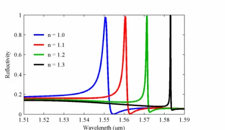
The configuration of a resonant SWG sensor is as shown in Fig. 2, but with the laser beam incident from the back side of the wafer. Backside illumination is advantageous because the front sensing surface is exposed to liquid analyte during operation. To suppress substrate Fabry-Pérot fringes in the reflection spectra, an antireflective coating is deposited on the backside. Figure 3 shows the reflectivity spectra of a resonant SWG sensor calculated by rigorous coupled wave analysis (RCWA)11 for four different values of the refractive index of the analyte liquid covering the grating surface. A structure consisting of a 200 nm thick SiO2 grating with a periodicity Λ = 1.24 µm and a duty ratio of 50% on a 0.22 µm thick silicon layer and a 3 µm thick buried oxide (BOX) layer was assumed. Reflectivity was calculated for p-polarized light incident from the back with an angle θ =45° (in air). The guided mode resonance features are well defined with a reflectivity approaching unity. A variation of the analyte index causes a change of the mode propagation constant of the TM mode in the silicon slab waveguide, as predicted by Eq. (3), resulting in a shift of the resonance wavelength. The induced resonance wavelength shifts shown in Fig. 3 correspond to a sensitivity of 110 nm per refractive index unit (RIU).
Fig. 3: Resonant subwavelength grating sensor reflectivity spectra calculated by RCWA for four different values of analyte liquid refractive index n.
Resonant SWG sensors were fabricated from commercial SOI substrates with 0.22 µm thick silicon and 3 µm thick BOX layers. The SiO2 gratings with a size of 5 mm × 7 mm, a thickness of 180 nm and various pitches around 1.24 µm were fabricated by plasma enhanced chemical vapor deposition (PECVD) of a SiO2 layer and subsequent patterning by optical lithography and plasma etching. A 150 mm diameter wafer with 112 gratings is shown in Fig. 4a. The backsides of the samples were polished and coated with a 9-layer AR coating consisting of alternating films of SiO2 and Nb2O5. A scanning electron microscope (SEM) image of a fabricated grating is shown in Fig. 4b.
Fig. 4: a) Photograph of a 150 mm diameter wafer with 112 resonant subwavelength grating sensors chip of size 5×7 mm2. b) SEM image of a SiO2 grating.
To confirm the predicted sensitivity of the resonant SWG sensors, we measured the resonance shift induced by flowing sucrose solutions of varying concentrations (and correspondingly varying refractive indices) over the sensor surface. For these measurements a plastic flow cell was attached to the sample surface by mechanical pressure and sealed with an O-ring. Suction from a syringe pump was used to deliver the various sucrose solutions to the flow cell volume. Reflectivity spectra were measured by scanning the wavelength of a tunable laser source over the spectral range of interest. An InGaAs photodetector was used to monitor the reflectivity as a function of wavelength. The angle of incidence of the laser beam was set in the optical setup at θ = 45°. To excite the TM mode of the slab waveguide, p-polarized light was used. Figure 5 shows the reflectivity spectra obtained for using de-ionized water (DIW) and three concentrations of sucrose as analyte. Changing the sucrose concentration by 1% corresponds to a refractive index change of 1.5×10⁻³. The total shift of approximately 0.5 nm observed in Fig. 5 for a 3% change in sucrose concentration thus corresponds to a sensitivity of 111 nm/RIU. This experimental result is in excellent agreement with the RCWA calculations discussed above.
Fig. 5: Bulk refractive index measurement using sucrose solutions of varying concentrations. The shift of the guided mode resonance is ~111 nm/RIU.
Fig. 6: Real-time sensing of streptavidin attachment to the waveguide surface.
We also carried out a protein sensing experiment using the prototypical biotin-streptavidin binding system. Results of the spectral shift of the guided mode resonance caused by the attachment of a monolayer of streptavidin measured in an air ambient were reported in ref [7]. The magnitude of this shift was found to be approximately 1 nm. In Fig. 6 we show a real time binding curve of streptavidin to a biotinylated SWG sensor surface. The sensor surface was prepared and functionalized as described in ref. [7] and, as in the sucrose solution measurements a flow cell was used to deliver phosphate buffer saline solution (PBS) and streptavidin to the sensor. The wavelength shift induced by the streptavidin attachment was measured by repeatedly scanning the tunable laser across the resonance and acquiring one reflectivity spectrum every 25 seconds. The shift as a function of time plotted in Fig. 6 was determined by tracking the peak position of each spectrum. The flow of the 0.05 mg/ml streptavidin in PBS solution was initiated at time t = 1350 s, followed by flushing with PBS for t > 2000 s. After the fast initial rise the peak shift saturates and then decreases slightly during the PBS rinse. The maximum peak shift, which we interpret as corresponding to the attachment of a complete monolayer of streptavidin, is 0.55 nm. This is smaller than the shift observed in air because the index contrast of the protein layer (n ~
1.5) and the ambient that it replaces is lower for measurements in water. The signal to noise ratio for this measurement is approximately 500, suggesting that the attachment of 0.2% of a monolayer of streptavidin is detectable.
3.
NON-RESONANT SUBWAVELENGTH GRATINGS
3.1 SWG waveguides
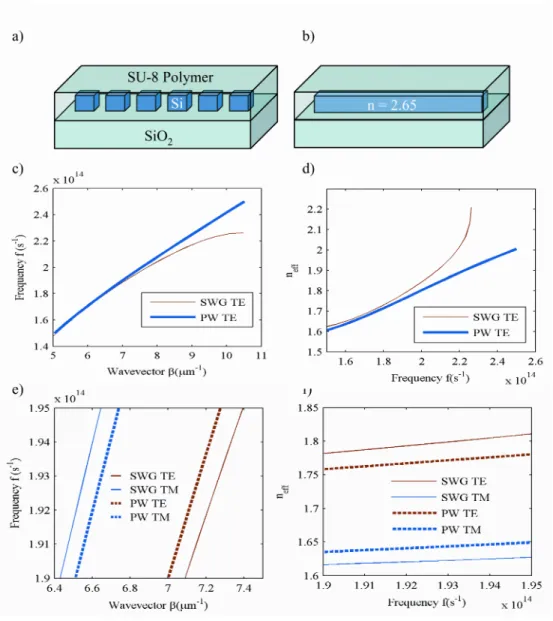
Silicon waveguides, the fundamental building blocks of silicon photonics, have been made with a wide range of cross-sectional sizes and geometries and with different cladding materials; however, the core refractive index of the waveguide is constant, i.e. the bulk material index of silicon. Effective medium theory, as discussed in the introduction, suggests that the core index can be tuned by subwavelength patterning of the waveguide, thus introducing a new degree of freedom in the design of silicon waveguides. As an example, an SWG waveguide structure is shown in a schematic view in Fig. 7a. The waveguide consists of a periodic array of rectangular segments of silicon on the BOX layer, covered by a cladding of SU-8 polymer with a refractive index of 1.58. The lateral size of each segment is 0.45 µm width × 0.26 µm height. The periodicity of the SWG is 0.3 µm, well below what would be required for a Bragg grating, and the duty cycle is 50%. According to effective medium theory one would expect this waveguide to behave optically like a 0.45 µm × 0.26 µm large photonic wire with a longitudinally averaged core refractive index, as shown in Fig. 7b. We have calculated the dispersion relation (frequency f versus wavevector β) and from it, the mode effective index, given by neff = cβ/(2πf) for both an SWG waveguide and a photonic wire with a core material index of 2.65. This particular core index was chosen to achieve an optimal match between the dispersion relations of the SWG and photonic wire waveguides for both polarizations at the operating wavelength of 1.55 µm, as shown below. The SWG waveguide dispersion was calculated using the MIT photonic bands software package12, while a commercial finite element mode solver was used for the photonic wire dispersion. The results are shown in Figs. 7c – 7f. In Fig 7c the dispersion relation for the TE mode of an SWG waveguide and a photonic wire are shown over a wide range of wavevectors. For β→ 10.5 cm-1 the SWG waveguide dispersion becomes flat, as the band gap of the periodic photonic structure is approached. The lower frequency cut-off of the stop band is f ≈ 226 THz corresponding to a vacuum wavelength λ = 1.33 µm. For the subwavelength region β << 10.5 cm-1 the dispersion of the SWG and photonic wire wavguides become closely matched. Fig. 7d shows the mode effective indices derived from the dispersion relation in Fig. 7c. An enlarged view of the dispersion relation and effective indices for both TE and TM polarized light around the operating wavelength of λ =
1.55 µm (f ≈ 193.5 THz) is shown in Figs. 7e and 7f. Clearly, there is a good correspondence between the SWG waveguide and its photonic wire equivalent, verifying the concept of core index tuning by subwavelength patterning. As one might expect, the agreement between SWG waveguide and effective photonic wire becomes even better when a smaller periodicity with the same duty cycle is chosen for the SWG. The effective core index of 2.65 is close to the value of 2.70 predicted by Eq. (1) using the indices of silicon and SU-8 for the SWG constituents.
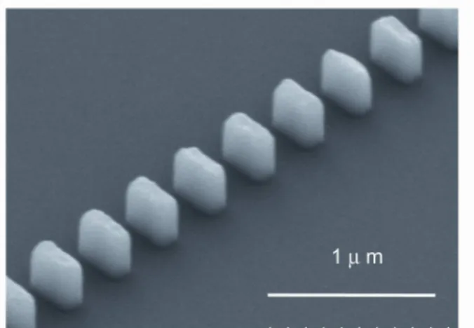
An SEM micrograph of a fabricated straight SWG waveguide is shown in Fig. 8. Samples were fabricated from commercial SOI substrates with 0.26 µm thick silicon and 2 µm thick BOX layers. We used electron beam lithography to define waveguide patterns in hydrogen silsesquioxane (HSQ) resist, which forms SiO2 upon electron beam exposure. The patterns were then transferred into the silicon layer by inductively coupled plasma reactive ion etching (ICP-RIE) using a mixture of SF6 and C4F8 gases. We coated the samples with a 2-µm-thick SU-8 polymer layer by a standard spin and bake procedure and finally cleaved them into individual chips. The facets were polished to an optically smooth finish.
We have found that the propagation loss of SWG waveguides with a cross section of 0.3 µm width × 0.26 µm height is approximately 2-3 dB/cm for both TE and TM polarized light. These values are lower than the loss of our standard photonic wire waveguides, which are typically in the 5-8 dB/cm range. We believe that the lower losses of the SWG waveguides are a consequence of the effectively lower index contrast between the core and the cladding, leading to mode delocalization and reduced light scattering efficiency of sidewall imperfections.
Fig. 7: a) SWG waveguide. b) Corresponding effective photonic wire waveguide with spatially averaged core material index. c) Comparison of dispersion relation for SWG and photonic wire (PW) waveguides (TE polarization). d) Corresponding effective mode indices. e) and f) Like c) and d) but for both polarizations and over a limited range of frequencies around 193.5 THz (corresponding to a free space wavelength of 1.55 µm).
Fig. 8: SEM micrograph of an SWG waveguide.
3.2 SWG waveguide fiber-chip couplers
SWG waveguides can be used for making efficient fiber-chip coupler structures for photonic wire waveguides. Compared to the now standard inverse taper coupling structures13 the tunability of the waveguide core index of SWG waveguides provides an additional parameter that can be used to optimize the mode matching between fiber and planar waveguide modes. SWG coupler structures, such as shown in the SEM micrograph in Fig. 9, were first proposed in ref. [14] and a first experimental demonstration was given in ref. [15]. This structure provides an adiabatic transition from a photonic wire waveguide (right side in Fig. 9) to an SWG waveguide (left). Recently we have further improved the coupler design. A more adiabatic transition is achieved by inserting silicon bridging elements in the center of the SWG waveguide, which increase gradually in width towards the photonic wire waveguide. The SWG waveguide is tapered and the duty cycle and period are chirped toward the chip edge to achieve an optimal match with the optical fiber mode. With this new design we have obtained significant improvements over the coupling efficiency reported in ref. [15]. For example, the TE coupling loss, which was measured to be approximately 6.5 dB in the previous design, is now estimated to be below 1 dB. Furthermore we have found that the SWG couplers have better fabrication tolerance with respect to waveguide width fluctuations. For example, a change in tip width from 350 nm to 300 nm leads to an excess loss of less than 0.1 dB for both polarizations.
Fig. 9: SEM micrograph of a photonic wire-SWG waveguide coupling structure. For fiber-chip coupling the SWG waveguide on the bottom left is extended to the chip edge with chirping of the grating parameters (period, duty cycle and width).
4.
SUMMARY AND CONCLUSIONS
In this paper we have described applications of both resonant and non-resonant silicon photonic SWG structures. A resonant SWG on the surface of an SOI waveguide couples the first diffraction order of an incident free space laser beam
to a waveguide mode, leading to a guided mode resonance in the specular reflectivity spectrum. We have used this effect to exploit the superior sensitivity of the TM mode of a 0.22 µm thick silicon waveguide for evanescent field sensing in a comparably simple optical configuration similar to established surface plasmon resonance sensing technology. We have demonstrated both bulk refractive index sensing using calibrated sucrose solutions and real-time sensing of protein attachment on a functionalized waveguide surface using the prototypical biotin-streptavidin binding system. We measured a bulk sensitivity of 110 nm/RIU, which is in good agreement with RCWA calculations and a wavelength shift of the resonance of ~0.55 nm for attachment of a monolayer of streptavidin with a signal to noise ratio of ~500 in the current optical setup.
We discussed applications of non-resonant SWGs. SWG waveguides consist of a periodic array of rectangular silicon segments. We have shown that the optical properties of these periodic waveguides are similar to photonic wire waveguides with a core refractive index averaged longitudinally along the structure as predicted by EMT. We have found that SWG waveguides have lower propagation losses compared to photonic wires. SWG coupler structures can be used at the chip edge as efficient fiber-to-photonic wire couplers with losses of less than 1 dB.
REFERENCES
[1] Mait, J. N. and Prather, D. W., Editors, “Selected papers on subwavelength diffractive optics,” SPIE Milestone Series volume MS 166 (2001).
[2] Kikuta, H., Toyota, H. and Yu, W., “Optical elements with subwavelength structured surfaces,” Opt. Review 10, 63-73 (2003).
[3] Rytov, S. M., “Electromagnetic properties of a finely stratified medium,” Sov. Phys. JETP 2(3), 466-475 (1956). [4] Joannopoulos, J. D., Johnson, S. G., Winn, J. N. and Maede, R. D., “Photonic crystals: Molding the flow of light”,
2nd edition, Princeton University Press, Princeton and Oxford (2008).
[5] Wang, S. S., Magnusson, R. and Bagby, J. S., “Guided mode resonances in planar dielectric-layer diffraction gratings,” J. Opt. Soc. Am. A 7(8) 1470-1474 (1990).
[6] Van Laere, F., Claes, T., Schrauwen, J., Scheerlinck, S., Bogaerts, W., Taillaert, D., O’Faolain, L., Van Thourhout, D. and Baets, R., “Compact focusing grating couplers for silicon-on-insulator integrated circuits”, IEEE Photon. Technol. Lett. 19(23), 1919-1921 (2007).
[7] Schmid, J. H., Sinclair, W., García, J., Janz, S., Lapointe, J., Poitras, D., Li, Y., Mischki, T., Lopinski, G., Cheben, P., Delâge, A., Densmore, A., Waldron, P. and Xu, D.-X., “Silicon-on-insulator guided mode resonant grating for evanescent field molecular sensing,” Opt. Express 17(20) 18371-18380 (2009).
[8] Densmore, A., Xu, D.-X., Waldron, P., Janz, S., Cheben, P., Lapointe, J., Delâge, A., Lamontagne, B., Schmid, J. H. and Post, E., “A silicon-on-insulator photonic wire based evanescent field sensor,” IEEE Photon. Technol. Lett. 18(23) 2520-2522 (2006).
[9] Densmore, A., Xu, D.-X, Janz, S., Waldron, P., Mischki, T., Lopinski, G., Delâge, A., Lapointe, J., Cheben, P., Lamontagne, B. and Schmid, J. H., “Spiral-path high-sensitivity silicon photonic wire molecular sensor with temperature-independent response,” Opt. Lett. 33(6) 596-598 (2008).
[10]Xu, D.-X., Densmore, A., Delâge, A., Waldron, P., McKinnon, R., Janz, S., Lapointe, J., Lopinski, G., Mischki, T., Post, E., Cheben, P. and Schmid J. H., “Folded cavity SOI microring sensors for high sensitivity and real time measurement of biomolecular binding,” Opt. Express 16(19), 15137–15148 (2008).
[11]Moharam, M. G. and Gaylord, T. K., “Rigorous coupled-wave analysis of planar-grating diffraction”, J. Opt. Soc. Am. 71(7), 811-818 (1981).
[12]http://ab-initio.mit.edu/wiki/index.php/MIT_Photonic_Bands.
[13]Almeida, V. R., Panepucci, R. R. and Lipson, M., “Nanotaper for compact mode conversion”, Opt. Lett. 28(15), 1302-1304 (2003).
[14]Cheben, P., Xu, D.-X., Janz, S. and Densmore, A., “Subwavelength waveguide grating for mode conversion and light coupling in integrated optics”, Opt. Express, 14(11) 4695-4702 (2006).
[15]Schmid, J. H., Cheben, P., Janz, S., Lapointe, J., Post, E., Delâge, A., Densmore, A., Lamontagne, B., Waldron, P., Xu, D.-X.,” Subwavelength grating structures in silicon-on-insulator waveguides,” Adv. Opt. Technol. volume 2008, Article ID 685489, doi:10.1155/2008/685489 (2008).