Block Copolymer Self-assembly and Templating Strategies
By
Wubin Bai
B.S., Physics (2011)
University of Science and Technology of China
Submitted to the Department of Materials Science and Engineering in
Partial Fulfillment of the Requirement for the Degree of
Doctor of Philosophy in Materials Science and Engineering
at the
Massachusetts Institute of Technology
June 2016
© 2016 Massachusetts Institute of Technology
All rights reserved
Signature of Author………...
Department of Materials Science and Engineering
May 2, 2016
Certified by……….
Caroline A. Ross
Professor of Materials Science and Engineering
Thesis Supervisor
Accepted by………
Donald Sadoway
Professor of Materials Chemistry
Chair, Department Committee on Graduate Student
Block Copolymer Self-assembly and Templating Strategies
By
Wubin Bai
Submitted to the Department of Materials Science and Engineering on
May 2, 2016 in Partial Fulfillment of the Requirement for the Degree of
Doctor of Philosophy in Materials Science and Engineering
Abstract
Block copolymers microphase separate to form periodic patterns with period of a few nm and above without the need for lithographic guidance. These self-assembled nanostructures have a variety of bulk geometries (alternating lamellae, gyroids, cylinder or sphere arrays, tiling patterns, core-shell structures) depending on the molecular architecture of the polymer and the volume fraction of its blocks. And in thin films, surface interaction and commensurability effect influence the self-assembly and result in more diverse morphologies including hexagonal-packed perforated lamellae, square array of holes. The progress of self-assembly can be tracked in situ using Grazing Incidence Small Angle X-ray Scattering, and the annealed morphology can be revealed in 3D using TEM tomography.
Moreover, non-bulk morphologies can be produced, the ordering of the microdomains can be improved and their locations directed using various templates and processing strategies. The blocks can themselves constitute a functional material, such as a photonic crystal, or they can be used as a mask to pattern other functional materials, functionalized directly by various chemical approaches, or used as a scaffold to assemble nanoparticles or other nanostructures. Block copolymers therefore offer tremendous flexibility in creating nanostructured materials with a range of applications in microelectronics, photovoltaics, filtration membranes and other devices.
TABLE OF CONTENTS
1 Introduction ···
11
1.1 Overview and Contents···11
1.2 Block Copolymer Thermodynamics···11
1.3 Nanolithography
···14
1.4 Conclusion
···17
2 Functional nanostructured materials based on
self-assembly of block copolymers
···21
2.1 Abstract
···21
2.2 Introduction
···21
2.3 Block Copolymers for Nanolithography
···22
2.4 Pattern transfer from 2D block copolymer films
···28
2.5 Block copolymer-based routes to 3D nanostructured
materials···29
2.6 Functional materials made from BCPs
···32
2.7 Summary
···36
3 Thin Film Morphologies of Bulk-Gyroid
Polystyrene-block-Polydimethylsiloxane
under
Solvent
Vapor
Annealing
···50
3.1 Abstract
···50
3.2 Introduction
···50
3.3 Materials and Methods
···51
3.4 Bulk morphology
···52
3.5 F i l m m o r p h o l o g y a s a f u n c t i o n o f a s - c a s t f i l m
thickness···53
3.6 S C F T M o d e l i n g o f f i l m t h i c k n e s s e f f e c t s o n
morphology···55
3.7 Film morphology as a function of solvent vapor composition
and swelling ratio···58
3.8 The effect of drying rate
···60
3.9 Defect analysis
···61
3.10
Self-consistent field theory simulations
···62
3.12 Pattern transfer using self-assembled nanostructure as a
mask
···70
3.13 Conclusions
···72
4 In Situ Characterization of the Self-assembly of a
Polystyrene-Polydimethylsiloxane
Block
Copolymer
during Solvent Vapor Annealing
···77
4.1 Abstract
···77
4.2 Introduction
···77
4.3 Experimental Methods
···79
4.4 Results and Discussion
···81
4.5 GISAXS data analysis
···96
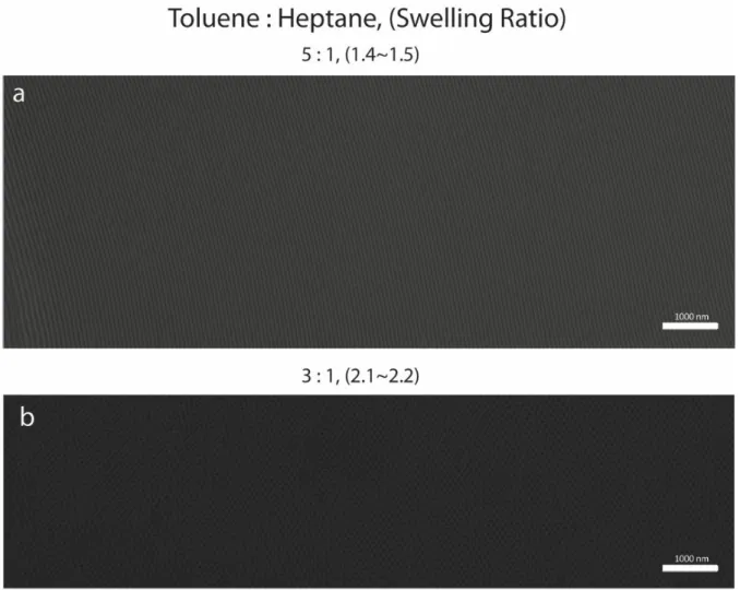
4.6 The Swelling Behavior of PS-PDMS in vapor from a Toluene:
Heptane 5:1 volumetric liquid mixture···97
4.7
Conclusion ···103
5 Templating Strategies to enable Orientation Control of
BCP Microdomains
···109
5.1 Abstract
···109
5.2 Introduction
···109
5.3 Experimental Methods
···110
5.4 Results and Discussion
···112
5.5 Other templating strategies
···123
5.6 Conclusion
···127
6 Conclusions and Future Works
6.1 Conclusions
···147
6.2 Future works
···149
LIST OF FIGURES
1. Introduction
Figure 1.1. Schematics of Block Copolymer self-assembly···12 Figure 1.2. Bulk morphology and Phase diagram of diblock copolymer···13 Figure 1.3. Schematic illustration of main steps of photolithography···15 Figure 1.4. Schematic illustration of main steps of imprinting lithography··162. Functional nanostructured materials based on
self-assembly of block copolymers
Figure 2.1. Representative SEMs of thin film self-assembled block copolymer structures···23 Figure 2.2. Directed self-assembly of BCPs···25 Figure 2.3. Controlling the orientation of microdomains···27 Figure 2.4. Pattern transfer from a BCP film···28 Figure 2.5. Sequential Self-assembly Processes···30 Figure 2.6. Functional materials made using block copolymers···333. Thin Film Morphologies of Bulk-Gyroid
Polystyrene-block-Polydimethylsiloxane
under
Solvent
Vapor
Annealing
Figure 3.1. SD75 Gyorid PS-PDMS Bulk Morphology···52Figure 3.2. Representative SEM images of PDMS microdomains formed in thin films with differing initial thickness at the same solvent vapor annealing condition···55
Figure 3.3. SCFT calculation of equilibrium film morphology of a bulk-gyroid block copolymer···57
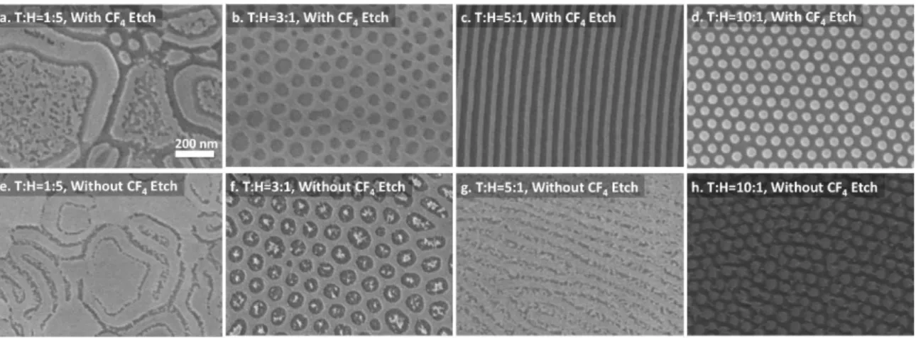
Figure 3.4. Representative SEM images of oxidized PDMS nanostructures with differing toluene: heptane (T:H) volumetric ratio in solvent annealing···58
Figure 3.5. Morphologies observed for as-spun film thickness = 45 nm under different solvent vapor annealing conditions···60
Figure 3.6. Fingerprint pattern, spiral pattern, and morphology after fast quench···61
Figure 3.7. Simulated SCFT equilibrium structures of the nanostructures formed in the bulk state. ···63
Figure 3.8. (a) A large area of cylinders. (b) A large area of Perforated Lamellae with initial as-cast film thickness 45 nm···64 Figure 3.9. (a), (c), Nearest Neighbor distance distribution; (b), (d), Pair-correlation function; (a), (b), Sphere phase; (c), (d), Hexagonal Perforated Lamellae phase···65 Figure 3.10. BCP films with films of thickness of ~90 nm annealed under vapor pressure (Ptol = 2.055 kPa, Phep =0.673 kPa) from a toluene: heptane 3:1 volumetric mixture at room temperature. ···66 Figure 3.11. AFM image of mixed morphologies (a, L and C, b, HPL and L). The interface between two phases (left: C+L, right HPL+L) corresponds to a terrace edge···67 Figure 3.12. Optical microscopy images of the unetched films with cylinder-lamella coexistence. ···68 Figure 3.13. Cylinder-Lamella coexistence observed at different solvent annealing conditions with swelling ratio around 1.5, as-cast film thickness 45 nm, 3-hour annealing. ···68 Figure 3.14. SD75 BCP films with initial film thickness 45 nm were annealed in various solvent mixtures. ···69 Figure 3.15. (a)Spheres observed for film thickness = 65 nm under 10:1 toluene: heptane volumetric ratio.(b)Top view SEM image of SD75 BCP with a region of cylinders at the left and interconnected structures at the right··70 Figure 3.16. The surface topography of ion beam patterned cobalt nanodots and nanowires imaged by scanning probe microscopy···80
4. In Situ Characterization of the Self-assembly of a
Polystyrene-Polydimethylsiloxane
Block
Copolymer
during Solvent Vapor Annealing
Figure 4.1. Process A: Solvent Vapor Annealing of a film of SD16 with as-spun thickness of 241 nm under solvent vapor produced from a toluene:heptane 5:1 volumetric mixture. ···83 Figure 4.2. GISAXS during the solvent absorption stage for three different solvent vapor pressures achieved by varying the gas flow through the bubbler or adding additional solvent into sample cell. ···85 Figure 4.3. SEM of final etched morphologies of films with different thickness···87 Figure 4.4. Evolution of the fractions of in-plane and out-of-plane oriented cylinders and the film swelling ratio with time in SD16 films···89 Figure 4.5. GISAXS measurements during solvent desorption for as-cast film thickness of 241 nm and solvent vapor evaporated from a Toluene: Heptane 5:1 volumetric mixture. ···91
Figure 4.6. Quantitative analysis of evolution of swelling ratio, microdomain spacing, and correlation length or grain size as function of time. ···94 Figure 4.7. In Situ GISAXS experimental set-up for block copolymer solvent vapor annealing···95 Figure 4.8. Swelling ratios of PS, PS-PDMS, and PDMS for different mole fraction of toluene in a toluene and heptane vapor mixture. ···99 Figure 4.9. GISAXS at the solvent-BCP concentration equilibration stage, in PS-b-PDMS films with as-cast film thickness 28 nm, 101 nm, 241 nm, 392 nm, 478 nm, 1141 nm, annealed under solvent vapor from a reservoir of Toluene: Heptane 5:1 volumetric mixture. ···100 Figure 4.10. In Situ swelling ratio of SD16 PS-b-PDMS thin film with as-cast film thickness 28 nm (process F) under solvent vapor produced from Toluene:Heptane 5:1 volumetric mixture. ···101 Figure 4.11. In situ swelling ratio of SD16 PS-b-PDMS thin film with as-cast film thickness 496 nm (process G) under solvent vapor produced from a Toluene:Heptane 5:1 volumetric mixture···102 Figure 4.12. GISAXS of a solvent-annealed SD16 PS-PDMS block copolymer film with as-cast thickness 241 nm. ···103
5. Perpendicular Block Copolymer Microdomains in High
Aspect-Ratio Templates
Figure 5.1. High Aspect-ratio Trenches Fabrication Process Flow···111 Figure 5.2. PDMS-brushed templates, solvent anneal···114 Figure 5.3. Templates with Pt base, solvent anneal···116 Figure 5.4. SEMs of perpendicular PS-PDMS lamellae in High Aspect-ratio···118 Figure 5.5. Thermal annealing···119 Figure 5.6. Free energy difference between vertical and horizontal lamellae···121 Figure 5.7. SCFT results···122 Figure 5.8. Self-assembled concentric BCP nanotubes···123 Figure 5.9. He-Ion microscope images of PS-b-PDMS after solvent vapor annealing···124 Figure 5.10. Directed Self-assembly of cylinder-forming BCp on cross-shape trenches···125 Figure 5.11. Directed Self-assembly of cylinder-forming BCP on multiple trenches···126
Acknowledgement
Thank you, our mentor Professor Caroline Ross for allowing me to be part of the journey with you. Your vision and inspiration make me excited about what I am doing everyday. You made every challenge in this journey a joyful adventure and a great opportunity for your students to grow. You introduced me to the wonderful community and gave me the chance to work with world-class researchers. I love doing research but I never thought I could be doing research at MIT and learning important life skills by doing or by trying. I am grateful for every interaction with teachers, labmates, collaborators, classmates, teammates, and friends both inside and outside MIT.
I would like to express my thankfulness to my other two thesis committees Professor Alfredo Alexander-Katz and Professor Niels Holten-Andersen, who have been supporting and guiding me in my PhD study. Thank you very much for opening the opportunity for collaborations, discussion in research ideas, and sharing the passion and wisdom about science and life! I truly appreciate the collaborations with Dr. Kevin Yager at Brookhaven National Lab, who hosted my every single visit to the synchrotron, one of the world most powerful research facilities. Your sharp mind and strong enthusiasm in science inspire me in designing experiments and solving challenging problems.
Thank you, all the members in Professor Caroline Ross’s group, for making Ross group such dynamic, collaborative and friendly place to explore interesting scientific questions. Karim Aissou, Kevin Gotrik, Adam Hannon, thank you for sharing your research experience and teaching me techniques and skills when I just joined the group. Karim Raafat Gadelrab, Christine Kathrein, Hyung Wan Do, Li-Chen Cheng, Kun-Hua Tu, Saman Safari Dinachali, Yi Ding, Thomas Lam, Hong Kyoon Choi, Jinshuo Zhang, Keehong Lee, Melissa Kreider, Nicolas Aimon, Dong Hun Kim, Astera Tang, Shuchi Ojha, Chen Zhang, Enno Lage, Pin Ho, Andy Quindeau, Eduardo Martin, Shuai Ning, I feel fortunate to have chance standing with you shoulder to shoulder. Thank you for bringing your incredible talents and maximum efforts into the projects and events organizing. Tim Savas, James Daley, Mark Mondol, Charlie Settens, Kurt Broderick, Patrick Boisvert, Shiahn Chen, Yong Zhang, Charlotte Stewart-Sloan, Mike Tarkanian, Ike Feitler, Alan Schwartzman, and Geetha Berera, thank you for giving me research facility trainings and helping me get through challenges. Thank you, Gabrielle, for your heartwarming care and tremendous help on our life and research.
It is my privilege to collaborate with famous pioneers from different fields. Professor Apostolos Avgeropoulos, George Liontos , Konstantinos Ntetsikas from University of Ioannina, Greece, Professor Ian Manners, Jessica Gwyther from University of Bristol, UK, thank you for keeping providing new synthesized materials for us to explore. Professor Alexander Böker, Dr. Larisa Tsarkova from RWTH Aachen University, Germany, Dr. J. Alexander Liddle from NIST, Professor
Karl Berggren from EECS MIT, Dr. Charles Black from BNL, Professor Carl Thompson, thank you for putting tremendous efforts in exploring new ideas and raising our work to a higher level. And I also would like to thank my undergrad advisor, Professor Tzay-Ming Hong, and Professor Shih-Lin Chang, who give me guidance, support and encouragement in my career development. I love you my family. Mom and dad, thank you for everything you do for your boy, thank you for supporting me with unconditional love and care. You let me do what I do and always encourage me to be better. You always set a great example for me in my career and my life. Xiaochen, thank you for always being there for me. The time with you is and will always be the best moments of my life. Wubin Bai
Chapter 1
Introduction
1.1 Overview and Contents
Synthesis of the nanoscale architectures with controlled chemical composition is essential in nanotechnology.1 Integrated fabrication is moving towards devices with
more computational power for less energy consumption.2 Memory storage media is
not only focusing on scaling down but also the design of device architecture, physical mechanism, and novel materials.3–5 Micro/Nanoelectromechanical systems
(MEMS or NEMS), and Biosensors require nanostructures with desired mechanical or biological properties.6,7 Battery cells, photovoltaics, photonic crystals and
filtration membranes also demand 3-dimensional nanostructures with controlled chemistry.8,9 Nanostructure fabrication strategies therefore need to become more
diverse to fit these different technologies.10,11 Among those fabrication routes, block
copolymer (BCP) self-assembly can form periodic nanostructures spontaneously with low cost and high efficiency,12,13 and directed self-assembly of BCPs can
produce device-oriented nanostructures with feature size from a few nanometers to hundreds of nm.14
This thesis focuses on fundamental understanding of the BCP self-assembly behavior and exploring templating strategies in order to fabricate device-oriented nanostructures. Chapter 1 briefly introduces thermodynamics of block copolymer and several nanofabrication techniques that are widely used. Chapter 2 generally reviews block copolymer self-assembly and its use for fabrication of functional nanostructures. Chapter 3 focuses on a Si-containing BCP thin film self-assembly using solvent vapor annealing and using it for pattern transfer into other functional materials such as metals. Chapter 4 discusses an in situ observation of the solvent vapor annealing and structural orientation control associated with annealing process. Chapter 5 shows the templating strategies in order to fabricate device-oriented nanostructure. Chapter 6 concludes the thesis and suggests future works.
1.2 Block Copolymer Thermodynamics
Block copolymers are macromolecules in which two or more chemically distinct repeat units are joined together in covalent bond. For example, a polystyrene-block-polymethylmethacylate (PS-b-PMMA) BCP consists of a PS chain covalently bonded to a PMMA chain. If the blocks are immiscible, the BCP can self assemble into periodic nanostructures with dimensions ranging from a few nm to several 100 nm.13,15–21 The
microphase-separated structure consists of “microdomains” of each block whose geometry depends on the volume fraction of the block and whose periodicity depends on the length of the polymer chain.12,22
The periodicity of the structure can range from a few nm to over 100 nm. A rich variety of nanostructures can be self-assembled based on the intrinsic properties of the blocks and the microdomain geometry, which is influenced by the polymer architecture, the annealing process (e.g. annealing by exposure to a solvent vapor environment or to an elevated temperature), and constraints such as those imposed by a patterned substrate.23–25
BCPs with two (e.g. diblock copolymers, Figure 1.1, or triblock copolymers) or three (e.g. triblock terpolymers) chemically distinct blocks are most commonly used, but incorporating further blocks and various architectures such as linear, star, cyclic or brush copolymers brings more diversity to both the properties and the morphology of the resulting self-assembled structure.26,27
Figure 1.1. Schematics of Block Copolymer self-assembly. (a) Self-assembled
morphology of a diblock copolymer, and the morphology revealed after etching one block. (b)-(d) Representative structures from block copolymer self-assembly. (b) lamellae; (c) cylinders, both from a diblock copolymer; (d) Archimedean tiling from a star terpolymer.
The phase behavior of a linear-shape diblock copolymer is governed by three experimentally controllable factors: the degree of polymerization N, the volume fraction of one block f, and the Flory-Huggins interaction parameter χ.13 N and f are
regulated through the polymerization stoichiometry and influence the translational and configurational entropy. The magnitude of χ is determined by the selection of chemically distinct monomers, contribute to the enthalpic part, and is dependent on the temperature 𝜒 ≈ 𝛼𝑇!!+ 𝛽, where 𝛼 > 0 and 𝛽 are constants for given values of
f. At equilibrium, a dense collection of monodisperse diblock copolymer chains will
be arranged in minimum free energy configurations. Increasing the interaction parameter 𝜒 (i.e. lowering the temperature) favors a reduction in contacts of distinct blocks. If N is sufficiently large, this may be accomplished with some loss of translational and configurational entropy by local compositional ordering (Figure 1.1). Such local segregation is referred to as microphase separation, and the local segregated domains are referred to as microdomains. Alternatively, if either 𝜒 or N is decreased enough, the entropic factors will dominate, leading to a compositionally disordered phase. Since the entropic and enthalpic contributions to the free energy density scale as N-1 and 𝜒, respectively, it is the product 𝜒𝑁 that determines the
linear-shape diblock copolymer phase state. Depending on the magnitude of 𝜒𝑁, the microphase separation can be weak segregation limit ( 𝜒𝑁~10) , or strong segregation limit (𝜒𝑁 ≫ 10).13 The phase diagram of a typical linear-shape diblock
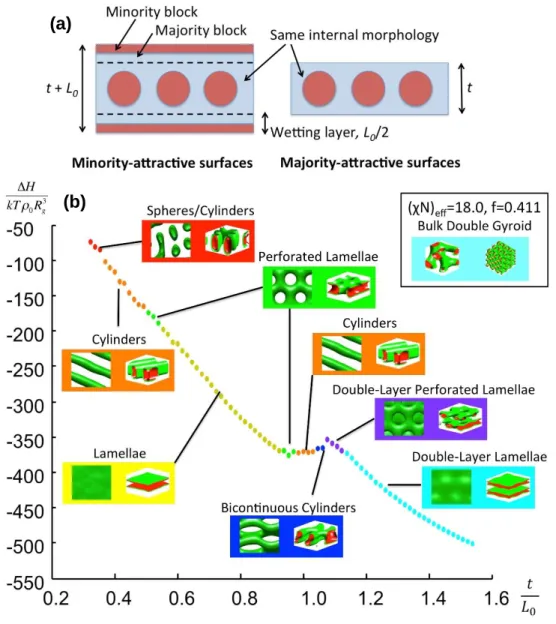
copolymer can be described by the “incompatibility degree” 𝜒𝑁 and the one independent composition variable (fA in Figure 1.2a), and consists of structures like spheres, cylinders, lamellae and gyroid. More details of BCP thermodynamics can be found in Ref. 13. Figure 1.2. Bulk morphology and Phase diagram of diblock copolymer. (a)
=body-centered-cubic spheres, C and C’ =hexagonally packed cylinders, G and G’ =bi-continuous gyroids, and L= lamellae. (b) Theoretical phase diagram of linear-shape diblocks predicted by the self-consistent mean field theory, depending on volume fraction (f) of the blocks and the segregation parameter, 𝝌𝑵, where 𝝌 is the Flory-Huggins segment-segment interaction energy and N is the degree of polymerization; CPS and CPS’ =closely packed spheres. (c) Experimental phase portrait of polyisoprene-block-polystyrene copolymers, in which fA represents the volume
fraction of polyisoprene, PL= perforated lamellae. Reproduced with permission from AIP, Ref. 12.
1.3 Nanolithography
Many applications are based on thin films of BCPs, and one of the most widely studied applications of thin film BCPs is in nanoscale lithography, where one block is removed by etching and the other is used as a mask to define features in a microelectronic device (Figure 1.1). More advanced BCP nanolithography techniques are realized based on combining BCP self-assembly with other widely-used lithography methods. Some of the lithography methods were briefly introduced here.
1.3.1
Photon-based Lithography
Photon-based lithography uses photon to transfer the space profile of photon intensity into a physical profile of a photoresist.28,29 Photon-induced chemistry
changes in the photoresist result in a solubility change of the resist when immersed in a specific solution which is called a developer, so that the developer can dissolve the region that was exposed to photons (Positive Tone Photoresist) or the unexposed regions (Negative Tone Photoresist) depending on the property of the photoresist. The basic steps in photolithography are illustrated in figure 1.3: (i) Exposure; (ii) Development; (iii) Etching.
Figure 1.3. Schematic illustration of main steps of photolithography. (i)
Exposure; (ii) Development; (iii) Etching.
In the exposure step (figure 1), the space profile of light intensity can be created by inserting a photomask between the light source and the sample. The photomask can be in physical contact with sample (Contact Printing), which results in high resolution, but damage of the mask and defects in the pattern can be induced by trapped fragments between the resist and the mask. To avoid this damage of the mask and the pattern, usually a small gap is kept between the mask and the sample (Proximity Printing), or projection lenses are inserted to both avoid the mask damage and achieve high resolution and uniformity (Projection Printing).
Interference lithography is a type of photolithography without using mask. In interference lithography, the space profile of light intensity is created by the interference between two or more coherent light waves.30–32 Typically, a coherent
laser beam passes through a spatial filter and interferes with a second coherent beam which is reflected from a mirror (Lloyd’s Mirror). A standing wave pattern is thus generated at which two beams intersect and record a grating image in the photoresist. The periodicity of the exposed grating can be tuned usually from 100 nm to 1500 nm by varying the wavelength of light (λ) and the half angle between the two beams (θ), as the equation: 𝑃 = λ (2sin ( θ)). More details on Interference Lithography can be found in Ref. 33.
There are many factors to influence the resolution of patterned features.34 Among
those factors, the wavelength of the light used has a critical effect because diffraction limits resolution. Therefore, the wavelengths of the light continue to decrease from ultraviolet (UV) to extreme UV or X-ray in order to fabricate denser integrated circuits in semiconductor industry.
1.3.2
Electron/Ion-based Lithography
Electron-beam or Ion-beam lithography can fabricate customized pattern with resolution as small as a few nm, which is far beyond the resolution of traditional
photolithography. In electron-beam lithography, a resist such as PMMA is used which is sensitive to electron. And cascades of secondary electrons cross-link resist or cause chain scission.35–37 Similarly, ion-beam lithography uses accelerated ion
beam to expose the resist on the substrate. In ion sculpting, the physical bombardment from the heavy ion removes materials from the film creating nanostructure.38 Furthermore, ion-beam lithography can also be employed for
depositing materials such as carbon, platinum, and tungsten.
1.3.3
Imprint and Scanning Probe Lithography
Imprint lithography utilizes a stamp to imprint a solution of molecules (ink) onto a substrate for pattern transferring.39–41 The stamp or mold can be soft material (such as cross-linked PDMS) or hard material (such as SiO2). Heating or UV curing may be adopted into imprinting lithography in order to facilitate the viscosity transition of the patterned film after the mold is applied. A schematic of the mechanism is illustrated in figure 1.2. Using a mold enables the large area patterns.
Scanning probe lithography uses the sharp probe in atomic force microscope to heat, scratch, oxidize or transfer substances to the surface of a substrate in order to produce nanostructures. Among these techniques, dip-pen nanolithography is widely used to create patterns directly on a range of substances with a variety of inks.42,43 Figure 1.4. Schematic illustration of main steps of imprinting lithography. (i) Apply Mold; (ii) Molding; (iii) Release Mold.
1.3.4
Self-Assembly Lithography
Self-assembly is a process in which structure formation is driven by internal interaction among the components themselves within the system.44–47 Meanwhile
structure. Self-assembly phenomena are found at all scales from the universe to a single atom. In nanolithography where interests are currently focused towards shrinking fabricated feature sizes, self-assembly is found particularly useful. In nanoscale fabrication, the idea of “building small hands in order to build small things” finds its limitation, as “smaller hands” become difficult to build. Following the mechanism of how nature multiplies herself, the idea of “structure builds itself” or self-assembly is attractive to explore.
Among those self-assembled systems which includes colloids, lipid bilayers, crystals, phase-separated polymers, and self-assembled monolayers, self-assembly of block copolymer became a classical system to study self-assembly mechanism and a promising material in nanostructure fabrication. A block copolymer is a polymer that covalently unites two or more different monomers, and its molecular architecture can be varied from linear, star-shape, or brush-shape, etc. If the blocks in the block copolymer are immiscible with each other, the block copolymer material tends to phase separate into microdomains to form periodic self-assembled structure. More details on BCP nanostructure fabrication and its application are explained in Chapter 2.
In this thesis work, a Si-containing BCP, polystyrene-block-polydimethylsiloxane
(PS-b-PDMS), is used to explore the self-assembly behavior. PS-b-PDMS is useful for
nanolithography applications due to the high etch selectivity between the PS and PDMS blocks,48–50 the etch resistance of the PDMS block, and the high χ parameter (χPS-PDMS ~
0.14-0.27 at room temperature).48,51 Self-consistent mean field theory simulation is used to predict the phase behavior of PS-b-PDMS self-assembly under different processing conditions or at different templating environment.
1.4 Conclusion
Block copolymer is a classical model to study the mechanism of self-assembly and also a promising material in application of nanolithography, in which other lithography methods could be integrated together with block copolymer lithography. But still, many challenges are remained to explore. Understanding the mechanism of self-assembly both experimentally and theoretically is essential to control the self-assembled nanostructure and lower its defects. Directed self-assembly of BCP is a key to produce device-oriented nanostructure, while templating strategies are still in the necessity of diversification both from fundamental mechanism and from advanced characterization. This thesis is trying to address those challenges by exploring the thin film behavior of a Si-containing BCP, the progress of its self-assembly using in situ observation method, and its templating effect using photon or electron beam patterned substrates or using electric field.
Reference
(1) Handbook of Nanostructured Materials and Nanotechnology, Five-Volume Set; Academic Press, 1999. (2) Mallik, A.; Ryckaert, J.; Mercha, A.; Verkest, D.; Ronse, K.; Thean, A. Maintaining Moore’s Law: Enabling Cost-Friendly Dimensional Scaling. In SPIE Advanced Lithography; Wood, O. R., Panning, E. M., Eds.; International Society for Optics and Photonics, 2015; p 94221N. (3) Mun, B. H.; You, B. K.; Yang, S. R.; Yoo, H. G.; Kim, J. M.; Park, W. I.; Yin, Y.; Byun, M.; Jung, Y. S.; Lee, K. J. Flexible One Diode-One Phase Change Memory Array Enabled by Block Copolymer Self-Assembly. ACS Nano 2015, 9 (4), 4120– 4128. (4) Wong, H.-S. P.; Raoux, S.; Kim, S.; Liang, J.; Reifenberg, J. P.; Rajendran, B.; Asheghi, M.; Goodson, K. E. Phase Change Memory. Proc. IEEE 2010, 98 (12), 2201–2227. (5) Wong, H.-S. P.; Lee, H.-Y.; Yu, S.; Chen, Y.-S.; Wu, Y.; Chen, P.-S.; Lee, B.; Chen, F. T.; Tsai, M.-J. Metal–Oxide RRAM. Proc. IEEE 2012, 100 (6), 1951–1970. (6) Rebeiz, G. M. RF MEMS: Theory, Design, and Technology; John Wiley & Sons, 2004. (7) Kirsch, J.; Siltanen, C.; Zhou, Q.; Revzin, A.; Simonian, A. Biosensor Technology: Recent Advances in Threat Agent Detection and Medicine. Chem. Soc. Rev. 2013, 42 (22), 8733–8768. (8) Goodenough, J. B.; Park, K.-S. The Li-Ion Rechargeable Battery: A Perspective. J. Am. Chem. Soc. 2013, 135 (4), 1167–1176. (9) Fahrenbruch, A.; Bube, R. Fundamentals Of Solar Cells: Photovoltaic Solar Energy Conversion; Elsevier, 2012. (10) Xia, Y.; Rogers, J. A.; Paul, K. E.; Whitesides, G. M. Unconventional Methods for Fabricating and Patterning Nanostructures. Chem. Rev. 1999, 99 (7), 1823– 1848. (11) Liddle, J. A.; Gallatin, G. M. Nanomanufacturing: A Perspective. ACS Nano 2016. (12) Bates, F. S.; Fredrickson, G. H. Block Copolymers—Designer Soft Materials. Phys. Today 1999, 52 (2), 32. (13) Bates, F. S.; Fredrickson, G. H. Block Copolymer Thermodynamics: Theory andExperiment. Annu. Rev. Phys. Chem. 1990, 41, 525–557. (14) Darling, S. B. Directing the Self-Assembly of Block Copolymers. Prog. Polym. Sci. 2007, 32 (10), 1152–1204. (15) Fasolka, M. J.; Mayes, A. M. BLOCK COPOLYMER THIN FILMS: Physics and Applications1. 2003. (16) Segalman, R. a. Patterning with Block Copolymer Thin Films. Mater. Sci. Eng. R Reports 2005, 48 (6), 191–226. (17) Park, C.; Yoon, J.; Thomas, E. L. Enabling Nanotechnology with Self Assembled Block Copolymer Patterns. Polymer (Guildf). 2003, 44 (22), 6725–6760. (18) Cheng, J. Y.; Ross, C. A.; Smith, H. I.; Thomas, E. L. Templated Self-Assembly of Block Copolymers: Top-Down Helps Bottom-Up. Adv. Mater. 2006, 18 (19), 2505–2521. (19) Bang, J.; Jeong, U.; Ryu, D. Y.; Russell, T. P.; Hawker, C. J. Block Copolymer Nanolithography: Translation of Molecular Level Control to Nanoscale Patterns. Adv. Mater. 2009, 21 (47), 4769–4792. (20) Ross, C. A.; Berggren, K. K.; Cheng, J. Y.; Jung, Y. S.; Chang, J.-B. Three-Dimensional Nanofabrication by Block Copolymer Self-Assembly. Adv. Mater. 2014, 26 (25), 4386–4396. (21) Nunns, A.; Gwyther, J.; Manners, I. Inorganic Block Copolymer Lithography. Polymer (Guildf). 2013, 54 (4), 1269–1284. (22) Hillmyer, M. Block Copolymer Synthesis. Curr. Opin. Solid State Mater. Sci. 1999, 4 (6), 559–564. (23) Chavis, M. A.; Smilgies, D.-M.; Wiesner, U. B.; Ober, C. K. Widely Tunable Morphologies in Block Copolymer Thin Films Through Solvent Vapor Annealing Using Mixtures of Selective Solvents. Adv. Funct. Mater. 2015, 25 (20), 3057–3065. (24) Tavakkoli K G, A.; Hannon, A. F.; Gotrik, K. W.; Alexander-Katz, A.; Ross, C. A.; Berggren, K. K. Rectangular Symmetry Morphologies in a Topographically Templated Block Copolymer. Adv. Mater. 2012, 24 (31), 4249–4254. (25) Sinturel, C.; Vayer, M.; Morris, M.; Hillmyer, M. A. Solvent Vapor Annealing of Block Polymer Thin Films. Macromolecules 2013, 46 (14), 5399–5415. (26) Bates, F. S.; Hillmyer, M. A.; Lodge, T. P.; Bates, C. M.; Delaney, K. T.; Fredrickson, G. H. Multiblock Polymers: Panacea or Pandora’s Box? Science 2012, 336 (6080), 434–440. (27) Börner, H. G.; Beers, K.; Matyjaszewski, K.; Sheiko, S. S.; Möller, M. Synthesis of Molecular Brushes with Block Copolymer Side Chains Using Atom Transfer Radical Polymerization. Macromolecules 2001, 34 (13), 4375–4383. (28) Willson, C. G.; Dammel, R. R.; Reiser, A. Photoresist Materials: A Historical Perspective. In Microlithography ’97; Tarascon-Auriol, R. G., Ed.; International
(29) Seisyan, R. P. Nanolithography in Microelectronics: A Review. Tech. Phys. 2011, 56 (8), 1061–1073. (30) Savas, T. a; Shah, S. N.; Schattenburg, M. L.; Carter, J. M.; Smith, H. I. Achromatic Interferometric Lithography for 100-Nm-Period Gratings and Grids. J. Vac. Sci. Technol. B (The 38th Int. Symp. electron, ion, Phot. beams) 1995, 13 (6), 2732– 2735. (31) Savas, T. A. Large-Area Achromatic Interferometric Lithography for 100 Nm Period Gratings and Grids. J. Vac. Sci. Technol. B Microelectron. Nanom. Struct. 1996, 14 (6), 4167. (32) Savas, T. A.; Farhoud, M.; Smith, H. I.; Hwang, M.; Ross, C. A. Properties of Large-Area Nanomagnet Arrays with 100 Nm Period Made by Interferometric Lithography. J. Appl. Phys. 1999, 85 (8), 6160. (33) Lu, C.; Lipson, R. H. Interference Lithography: A Powerful Tool for Fabricating Periodic Structures. Laser Photon. Rev. 2009, 4 (4), 568–580. (34) Harriott, L. R. Limits of Lithography. Proc. IEEE 2001, 89 (3), 366–374. (35) WATT, F.; BETTIOL, A. A.; VAN KAN, J. A.; TEO, E. J.; BREESE, M. B. H. ION BEAM LITHOGRAPHY AND NANOFABRICATION: A REVIEW. Int. J. Nanosci. 2005, 04 (03), 269–286. (36) Pease, R. F. W. Electron Beam Lithography. Contemp. Phys. 2006, 22 (3), 265– 290. (37) Tseng, A. A.; Chen, C. D.; Ma, K. J. Electron Beam Lithography in Nanoscale Fabrication: Recent Development. IEEE Trans. Electron. Packag. Manuf. 2003, 26 (2), 141–149. (38) Li, J.; Stein, D.; McMullan, C.; Branton, D.; Aziz, M. J.; Golovchenko, J. A. Ion-Beam Sculpting at Nanometre Length Scales. Nature 2001, 412 (6843), 166– 169. (39) Chou, S. Y.; Krauss, P. R.; Renstrom, P. J. Imprint of Sub-25 Nm Vias and Trenches in Polymers. Appl. Phys. Lett. 1995, 67 (21), 3114. (40) Resnick, D. J.; Sreenivasan, S. V.; Willson, C. G. Step & Flash Imprint Lithography. Mater. Today 2005, 8 (2), 34–42. (41) Rogers, J. A.; Nuzzo, R. G. Recent Progress in Soft Lithography. Mater. Today 2005, 8 (2), 50–56. (42) Ginger, D. S.; Zhang, H.; Mirkin, C. A. The Evolution of Dip-Pen Nanolithography. Angew. Chem. Int. Ed. Engl. 2004, 43 (1), 30–45. (43) Piner, R. D. “Dip-Pen” Nanolithography. Science (80-. ). 1999, 283 (5402), 661–663. (44) Hawker, C. J.; Russell, T. P. Block Copolymer Lithography: Merging “Bottom-Up” with “Top-Down” Processes. MRS Bull. 2011, 30 (12), 952–966. (45) Black, C. T.; Ruiz, R.; Breyta, G.; Cheng, J. Y.; Colburn, M. E.; Guarini, K. W.; Kim, H.-C.; Zhang, Y. Polymer Self Assembly in Semiconductor Microelectronics.
IBM J. Res. Dev. 2007, 51 (5), 605–633. (46) Black, C. T. Polymer Self-Assembly as a Novel Extension to Optical Lithography. ACS Nano 2007, 1 (3), 147–150. (47) Yan, H.; Park, S. H.; Finkelstein, G.; Reif, J. H.; LaBean, T. H. DNA-Templated Self-Assembly of Protein Arrays and Highly Conductive Nanowires. Science 2003, 301 (5641), 1882–1884. (48) Nose, T. Coexistence Curves of Polystyrene/ Poly(dirnethylsiloxane) Blends. Polymer (Guildf). 1995, 36 (11), 2243–2248. (49) Jung, Y. S.; Ross, C. A. Orientation-Controlled Self-Assembled Nanolithography Using a Polystyrene-Polydimethylsiloxane Block Copolymer. Nano Lett. 2007, 7 (7), 2046–2050. (50) Son, J. G.; Gotrik, K. W.; Ross, C. A. High-Aspect-Ratio Perpendicular Orientation of PS- B -PDMS Thin Films under Solvent Annealing. ACS Macro Lett. 2012, 1 (11), 1279–1284. (51) Kennemur, J. G.; Yao, L.; Bates, F. S.; Hillmyer, M. A. Sub-5 Nm Domains in Ordered Poly(cyclohexylethylene)- Block -Poly(methyl Methacrylate) Block Polymers for Lithography. Macromolecules 2014, 47 (4), 1411–1418.
Chapter 2: Functional nanostructured materials based on
self-assembly of block copolymers
2.1 Abstract
In this chapter, we review the self-assembly of block copolymer in thin films and in bulk and discuss the self-assembly strategies to fabricate functional
nanostructures. Block copolymers microphase separate to form periodic patterns with period of a few nm and above without the need for lithographic guidance. These self-assembled nanostructures have a variety of bulk geometries
(alternating lamellae, gyroids, arrays of cylinders or spheres, tiling patterns, core-shell structures) depending on the molecular architecture of the polymer and the volume fraction of its blocks. Moreover, non-bulk morphologies can be produced, the ordering of the microdomains can be improved and their locations directed using various templates and processing strategies. The blocks can themselves constitute a functional material, such as a photonic crystal, or they can be used as a mask to pattern other functional materials, functionalized directly by various chemical approaches, or used as a scaffold to assemble nanoparticles or other nanostructures. Block copolymers therefore offer tremendous flexibility in
creating nanostructured materials with a range of applications in microelectronics, photovoltaics, filtration membranes and other devices. This work was published in Ref. [1]
2.2 Introduction
Block copolymers can be used in a wide range of applications,2,3
constituting functional materials themselves by virtue of the properties of the blocks, or by selectively etching4,5
one block to form masks or templates for the synthesis of functional materials. BCPs can include organic coil-like blocks, liquid crystalline blocks, Si- or metal-containing blocks, biological blocks, and/or conductive blocks providing a multitude of properties.6–9
The BCP nanostructure can be altered by several chemical methods such as sequential infiltration synthesis (SIS) which introduces metals or oxides from a precursor as in chemical vapor
deposition;10,11
by salt complexation;12,13
or by nanoparticle incorporation.14,15 In this review, we will first discuss the applications of thin film BCPs in
required. We will then discuss three-dimensional BCP assemblies. We show that BCP nanostructures have applications in fabrication of integrated circuits,16,17 magnetic storage media,18–20
sensors,21–24
photonic crystals,25–27
photovoltaics28–30 and separation membranes,31,32
as well as for making 3-dimensional nanostructures.33
2.3 Block Copolymers for Nanolithography
In nanolithography, a film of a BCP is prepared on a substrate and one of the blocks is removed. The remaining structure serves as a mask for pattern transfer into a metal, dielectric or other material. This can be carried out using the
microdomain pattern made from an untemplated block copolymer film, producing a dense array of dots, holes or lines. However, the greatest efforts have been expended in developing BCP nanolithography for nanoscale electronic devices, where precise registration and reproducibility of the self-assembled
nanostructures and low defect levels are essential. Conventional 193 nm wavelength photolithography feature sizes are limited by diffraction, although sub-lithographic feature sizes may be obtained by complex double or quadruple patterning processes. However, 193 nm lithography is unlikely to produce features below about 20 nm dimensions, and directed self-assembly (DSA) of block copolymers has become a candidate planar process for semiconductor device nanofabrication, according to the International Technology Roadmap for Semiconductors.
The period of the microphase-separated BCP structure is governed by the polymer chain length and hence the degree of polymerization, N (the number of monomers constituting the chain) but the driving force for self-assembly is governed by the product χN where χ is the Flory-Huggins interaction parameter quantifying the incompatibility between the blocks. Therefore, high χ is desirable to obtain features with small period from BCPs with low N. BCPs which yield feature period below 10 nm can microphase-separate at room temperature if χ is high enough,34–36
or by design of the macromolecular architecture (such as brush BCPs). This makes BCP lithography an attractive path to continued device
miniaturization.
BCP thin films can be spin-coated from solution like a resist layer, annealed using a hotplate at moderate temperatures or by placing them in a solvent vapor, and etched by reactive ion etching, making them compatible with conventional semiconductor fabrication technology.37–39
Diblock copolymer films on
closepacked spheres, in-plane or out-of-plane-oriented cylinders or lamellae, perforated lamellae, or gyroids, by controlling the block volume fraction40
and the annealing process.11,13,41–45
More diverse morphologies can be produced from triBCPs (or multi-BCPs),14,46,47
mixtures of diBCPs,48
or multi-BCPs blended with homopolymer. 18,46
For example, square arrays were achieved by using triblock terpolymer/homopolymer blends, 18,49
Archimedean tiling patterns were produced from a 3-miktoarm star terpolymer (a star-shaped polymer where 3 different polymer arms emanate from a core),46
and blended morphologies between spheres and perforated lamellae were demonstrated by blending a Si-containing BCP with an iron-containing BCP.48
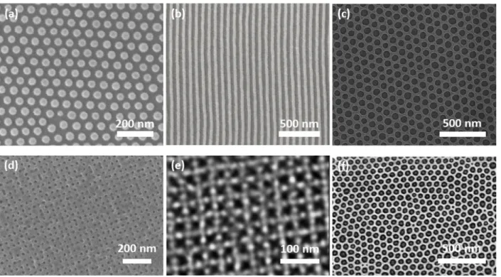
Examples of thin film BCP morphologies are given in Figure 2.1. Figure 2.1. Representative SEMs of thin film self-assembled block copolymer structures. (a) Monolayer of spheres; (b) cylinders; (c) perforated lamellae; (a), (b), (c) are from a bulk gyroid-forming polystyrene-block-polydimethylsiloxane (PS-b-PDMS) with molecular weight 75.5 kg/mol, and volume fraction fPDMS=0.415; (a), (b) (c) Reproduced with permission.41 Copyright 2014, ACS Publications; (d) Square array of holes, from a linear triblock terpolymer polyisoprene-b-polystyrene-b-polyferrocenylsilane (PI-b-PS-b-PFS) with volume fractions of 25%, 65%, and 10%, respectively, and total molecular weight 82 kg/mol, blended with Polystyrene homopolymer; Reproduced with permission.47 Copyright 2012 ACS Publications; (e) Archimedeam tiling pattern, from a 3-
miktoarm star terpolymer (polyisoprene-arm-polystyrene-arm-polyferrocenylethylmethylsilane with volume fractions of 39%, 35%, 26%, respectively, and total molecular weight 66 kg/mol) blended with polystyrene homopolymer; Reproduced with permission.46 Copyright 2013, ACS Publications; (f) Hierarchical nanostructure, from blend of a polydimethylsiloxane-b- polystyrene (PDMS-PS, MW=45.5 kg/mol, fPDMS=33.7%) and a polystyrene-b-polyferrocenyldimethylsilane (PS-PFS, MW=35 kg/mol, fPFS=11.5%). Reproduced with permission.48 Copyright 2013, Nature Publishing Group.
The microdomain patterns formed in thin films of BCPs possess short-range order but lack long-range order, as seen in some of the images of Figure 2. A top-down method can be employed to guide BCP self-assembly, providing registration and alignment with features in the substrate, and minimizing the defectivity.
Graphoepitaxy and chemoepitaxy are the two main templating strategies for DSA50–55
using confinement-induced structural frustration and interfacial interactions respectively to control BCP self-assembly. This can produce well-ordered periodic arrays as well as aperiodic structures not found in bulk.56–60 Topographical templates include small posts fabricated by electron-beam lithography, functionalized to be attractive to one block,61
or trenches fabricated by photolithography or interference lithography;62–65
whereas chemoepitaxy templates consist of chemically distinct regions of the substrate that are attractive to one or other block, such as stripes, bends, dots and other features 66–68
. In both graphoepitaxy and chemoepitaxy, pattern multiplication has been demonstrated, i.e. the density of templating features can be less than the final density of the BCP pattern.51,66,78
To optimize the templates in order to produce desired self-assembled BCP geometries, inverse design algorithms combined with self-consistent field theory (SCFT) simulations have been developed, in which SCFT can predict the BCP morphologies at conditions of film thickness, topographic confinements, and surface energy.16,69–72
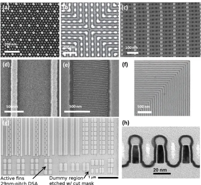
Figure 2.2 shows examples of BCP films templated by graphoepitaxy (Fig. 2.3a-e,g,h) and chemoepitaxy (Fig. 2.3f). Scaleup of these processes to wafer level using templates made by photolithography has been demonstrated.73–75
Figure 2.2. Directed self-assembly of BCPs. (a) SEM of ordered BCP spheres formed within a sparse 2D lattice of HSQ posts (brighter dots). The substrate and post surfaces were functionalized with a PS brush layer; Reproduced with permission.51 Copyright 2008, AAAS. (b) By using an array of dashes oriented in the x- and y- directions, nested-elbow structures form with a cross-point junction in the center; Reproduced with permission.76 Copyright 2010, Nature Publishing Group; (c) SEM of an etched 3D bilayer structure on a substrate. The bright dots and the light gray linear features represent HSQ and oxidized-PDMS, respectively; Reproduced with permission.61 Copyright 2012, AAAS; (d) SEM of parallel cylinders on a trenched substrate with narrow mesas (width Wmesa=125 nm and Wtrench= 875 nm) annealed under a high vapor pressure of toluene. (e) SEM of perpendicular cylidners in a wide mesa pattern (Wmesa=270 nm and Wtrench=730 nm) at a lower vapor pressure. (d), (e) reproduced with permission.77 Copyright
2007, ACS Publications (f) Top-down SEM of 90o-angled lamellae from chemoepitaxy of a ternary PS-b-PMMA/PS/PMMA blend. Reproduced with permission.78 Copyright 2005, AAAS (g) Directed self-assembly of lamellar phase PS-b-PMMA BCP to form line-space circuit patterns in order to fabricate Si fin features; (h) A transmission electron microscope image of 29 nm pitch silicon on insulator fins formed by BCP directed self-assembly. (g), (h) reproduced with permission.63 Copyright 2014, ACS Publications.
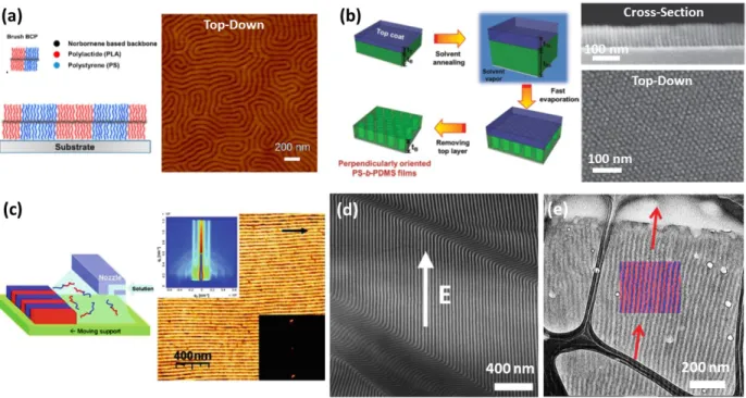
As mentioned above, a high χ is desirable to obtain microdomains with small period. However, high-χ BCPs usually exhibit large differences in surface energy between the blocks, leading to the formation of a layer of the lower surface energy block at the air interface, and favoring in-plane orientation of lamellar or cylindrical microdomains. Perpendicularly-oriented microdomains provide higher aspect ratio features that facilitate pattern transfer, and can be promoted by a neutral coating,79,80
a comb-like polymer architecture, 81
and processing under external conditions including electric field, 82–84
magnetic field,85 temperature gradient, 86–88 solvent gradient, 80,89,90 shear, 91,92,93 zone casting,94 Electrohydrodynamic Jet Printing95
or electrospray deposition96
. Figure 2.3 shows examples of the alignment of BCP microdomains perpendicular to the substrate. In contrast to the precise and intricate structures formed by DSA, some
applications only require short-range-ordered nanostructures with or without a common orientation. This is straightforward to accomplish by BCP thin film self-assembly. Examples include porous dielectrics97,98
such as the IBM Airgap,99 filtration membranes or water desalination membranes,100
some photovoltaic membranes,101,102 and electrodes for batteries.103,104
Figure 2.3. Controlling the orientation of microdomains. (a) Lamellar microdomains oriented perpendicular to the substrate from the self-assembly of a brush BCP, Left: schematic, Right: AFM; Reproduced with permission.81 Copyright 2013, ACS Publications; (b) The solvent annealing process of block copolymer thin films with a top coat layer to produce a perpendicular orientation of the microdomains. Top coats were carefully chosen for solvent permeability during solvent annealing and were simply removed with a non-solvent for both blocks of the BCP. Left: schematic, Right: SEM of cross-section and top-down view; Reproduced with permission.80 Copyright 2014, Wiley-VCH; (c) Zone casting method to direct the self-assembly of BCPs; Left: semicrystalline lamellar poly(octadecyl methacrylate)-b-Poly(t-butyl acrylate)-b-Poly(octadecyl methacrylate) (PODMA-b-PtBA-b-PODMA) system above and below melting point. Right: AFM images and GISAXS patterns of aligned microdomains. Arrow indicates casting direction. Reproduced with permission.94 Copyright 2011, ACS Publications; (d) Electric-field-induced alignment of block copolymer microdomains. TEM image of lamellar-forming polystyrene-block-polyisoprene (SI) BCP morphology after electric-field alignment. Reproduced with permission.105 Copyright 2002, APS; (e) The electrospray process of polystyrene-b-polybutadiene-b-polystyrene (SBS) triBCP. Small droplets containing SBS are generated from a charged atomizer and transported onto heated substrate. Arriving SBS particles equilibrate with the substrate and adopt out-of-plane morphology dictated by the strong evaporation of solvent. Crosslinking of PB
occurs simultaneously with ordering as the film undergoes thermal annealing, preserving the vertical alignment of the film. Reproduced with permission.96
Copyright 2015, Wiley-VCH.
2.4 Pattern transfer from 2D block copolymer films
In some applications the BCP film itself forms the functional material, such as a porous dielectric formed by etching a BCP film, but in many cases the BCP film is used as a sacrificial mask for patterning another material.33,106–109
Monolayers of in-plane cylinders or spheres, perpendicular cylinders and lamellae, and
perforated lamellae are particularly suitable for pattern transfer. Pattern transfer takes advantages of the methods developed for planar processing, including additive (e.g. liftoff) and subtractive (etching) methods. Figure 2.4 shows how these processes were applied to pattern dots of Co using a polystyrene-block-polydimethylsiloxane (PS-b-PDMS) BCP. Figure 2.4. Pattern transfer from a BCP film. (a) Left: Schematic of liftoff from a BCP mask using a sacrificial PMMA underlayer, Right: SEM of cobalt nanodots fabricated by lift-off process. Inset: tilted views illustrate edge tapering; (b) Left: Schematic of Damascene pattern transfer process from BCP to metal nanostructure. Right: SEM of cobalt nanodots transferred from a PS-b-PDMS perforated lamellar structure; (c) Left: Schematic of subtractive pattern transfer process from BCP self-assembled mask by ion-beam etch process. Right: Plan view and cross-sectional SEM showing the cobalt nanodots transferred from a
perforated lamellar pattern using a hard mask of tungsten. Reproduced with permission.108 Copyright 2015, IOPscience
Etching an underlying material through a BCP mask allows pattern transfer into many materials including multilayers or epitaxial structures that cannot be grown on top of the BCP mask.108,110,111
The success of the etching process depends on the etch contrast between the BCP mask and the material, the aspect ratio of the mask, the relative thicknesses of the layers, and available etch chemistries for the material. Reactive ion etching or ion-beam etching are typically used, and the BCP pattern may first be transferred into a hard mask such as a heavy metal (Ta, W, etc.) or hard carbon which has greater durability than the BCP film during the etch of the functional material.
Additive patterning has also been widely applied including electrodeposition, lift-off and damascene processes.18,112
Lift-off involves depositing the functional material onto a soluble BCP pattern with vertical or undercut pores using a collimated vapor deposition process such as evaporation to produce well-defined edge morphologies of the deposited material. Dissolving the BCP pattern removes the material on top of it, leaving only the material that was deposited on the substrate at the bottom of the pores. The solubility of the BCP can be improved, and the pore aspect ratio and sidewall undercut enhanced, by using a sacrificial layer such as PMMA inserted between the BCP film and the substrate, which is etched through to the substrate in the locations of the BCP pores. In a damascene process,111
the functional material is deposited over BCP topographical features then etched back and planarized by, for example, reactive ion etching. Etching is stopped once it has reached the BCP features, leaving the functional material within the pores of the BCP film. The remaining BCP can then be selectively removed.113
2.5 Block copolymer-based routes to 3D nanostructured materials
So far we have discussed 2D or planar processing where a layer of BCP microdomains is used to pattern a film or surface. BCPs can also produce 3D structures which can be built up from 2D layers, or which can be formed in one step from thick film or bulk BCPs with multiple layers of microdomains. One class of synthetic routes involves building a 3D functional material from stacks of 2D layers or by repeatedly templating one BCP on another.33
Independent BCP layers can be stacked by separating them, for example using a graphene or silicon layer in between the layers.114,115
The orientation of microdomains in different layers can be controlled independently by shear alignment induced by a laser pulse, solvent incorporation, a thermal gradient, or direct mechanical shear. This has been used to make lattice structures with arbitrary symmetries from a cylinder-forming BCP.116,117
Sequential self-assembly processes use the etched self-assembled BCP microdomains of a lower layer as a new template for an upper layer of the same or different BCP, which can result in a wide range of novel 3D nanostructures.118
The orientation of one layer of cylinders on another one can be controlled by the substrate chemistry and topography.119
Meshed structures consisting of two layers of cylinders at an angle to each other can also be made in one step by suitable templating.71,120
Figure 2.5 shows examples of these structures.
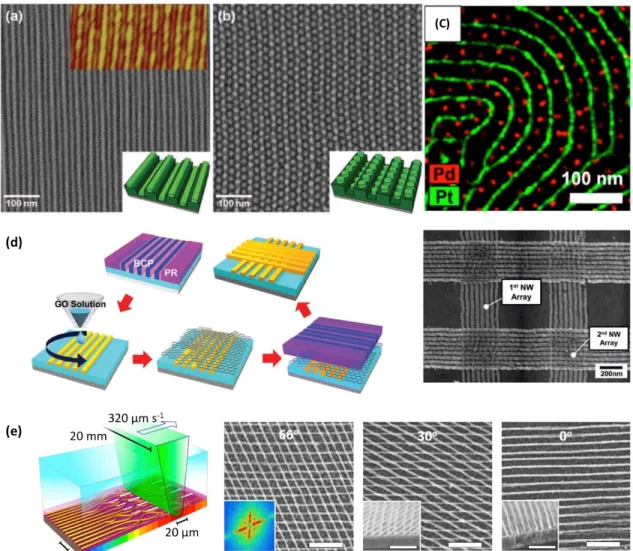
Figure 2.5. Sequential Self-assembly Processes. (a) Hierarchical line-on-line structures made from 16 kg mol-1 PS-b-PDMS line patterns on 45 kg mol-1 line
patterns. (b) Self-assembly of 16 kg mol-1 PS-PDMS dot patterns on 45 kg mol-1 PS-b-PDMS line patterns forming a dots-on-line structure. (a), (b) reproduced with permission.118 Copyright 2011, Wiley-VCH; (c) Multicomponent nanopatterning and elemental mapping of Pt nanowire-Pd nanodot array made using sequential BCP self-assembly. Reproduced with permission.121 Copyright 2013, ACS Publications; (d) Left: Schematic showing independent control of a double layer of BCP microdomains by inserting a graphene layer in between the BCP layers. Right: Al nanowire crossbar array made from double layers of orthogonally directed self-assembly; Reproduced with permission.114 Copyright 2013, Wiley-VCH; (e) Soft-shear laser zone annealing (SS-LZA). SS-LZA is used to produce aligned BCP templates for nanowire synthesis. Experimental schematic: a focused laser line is absorbed by a layer of germanium underlying a BCP film, inducing local heating and high thermal gradients. At the same time the thermal expansion of an overlaid PDMS sheet shears and aligns the BCP. Reproduced with permission.117 Scale bars 200 nm. Copyright 2015, Nature Publishing Group.
3D BCP structures can be obtained from bulk BCPs or from films thick enough to show periodic structures in the out of plane direction. BCPs confined in pores with cylindrical or spherical shape show a diversity of non-bulk 3D
structures,57,122–124
for example helical, toroidal or concentric cylindrical morphologies.123
Converting these 3D morphologies into functional materials can be done by a variety of methods. One block can be replaced by another material, for example by etching it and backfilling by electrodeposition,116,125 or by selectively
depositing material by SIS10
or chemical reduction. SIS uses precursors such as those used in chemical vapor deposition: TiCl4, AlCl3, Al(CH3)3, etc.
126
Chemical reduction of precursors took place in the poly(ethylene oxide) microdomains of a cylinder-forming polystyrene-block-poly(ethylene oxide) (PS-b-PEO) BCP, which tuned the material chemistry of the resulting self-assembled nanostructure and changed the microdomain orientation.12
Nanoparticles such as Au can be formed within poly-4-vinylpyridine blocks by reduction of salts.127
Alternatively nanoparticles can be synthesized separately and blended with the BCP during casting to produce a co-assembled structure.27,28,128
The nanoparticles can be located within the microdomains or at the interfaces. As an example a blend of Au nanoparticles capped with 1-dodecanethiol and a cylinder-forming
polystyrene-block-poly-4-vinylpyridine (PS-b-P4VP) BCP hydrogen-bonded to
hexagonally packed 3D structures in which the Au nanoparticles were selectively located at the interstitial sites in the P4VP matrix.129
2.6 Functional materials made from BCPs
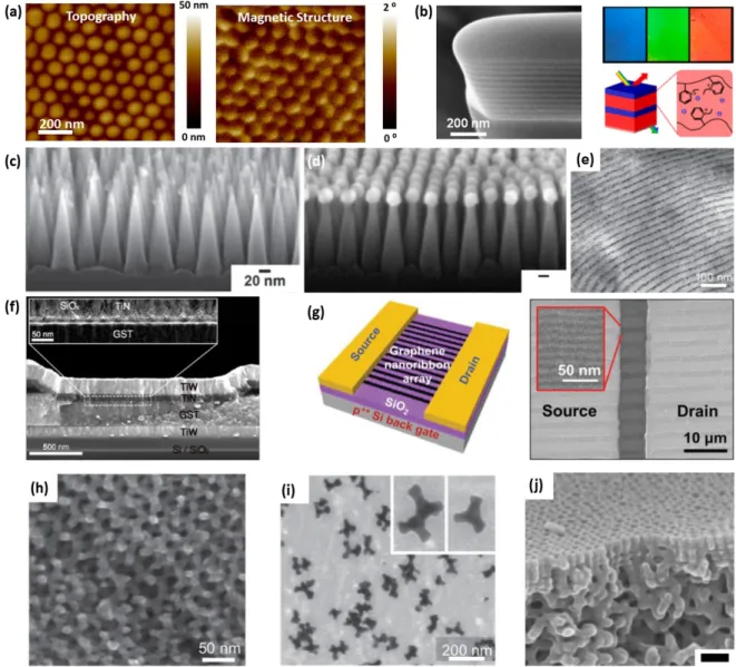
Nanostructured films made by pattern transfer from a BCP layer using planar processing have exhibited a wide range of interesting and useful properties.130 Some examples of these structures are given in Fig. 2.6. For example,
considerable effort has been applied to patterning of magnetic films for patterned media applications. The magnetic anisotropy, magnetic domain structure and reversal process are dominated by the shape and size of the features as well as the material properties. Arrays of magnetic dots, rings or pores have been made from various magnetic alloys. 33,131–133
A recent study compared the properties of Co dots made by additive and subtractive methods using the same BCP, determining that etching produced the smallest switching field distribution.108
Bit patterned media with area density beyond 1.5 teradot/inch2
was achieved by pattern transfer from an ordered BCP.133
Figure 2.6. Functional materials made using block copolymers. (a) Left: The surface topography of ion-beam etched cobalt nanodots imaged by scanning probe microscopy, Right: The corresponding magnetic structure of the patterned nanodots showing in-plane magnetization; Reproduced with permission.108 Copyright 2015, IOPscience; (b) Left: Cross-Sectional SEM (52o tilt) of a focused ion beam milled dry PS-b-QP2VP lamellar film. To enhance the layer contrast, the films were exposed to iodine vapor for a selective staining of the QP2VP layers, resulting in brighter layers. Right: Schematic representation of the mechanism for color change in a PS-b-QP2VP photonic lamellar gel by a direct exchange of counterions leading to swelling. Reproduced with permission.134 Copyright 2012, ACS Publications; (c) Side-view SEM of a silicon superhydrophobic surface textured with nanocones; Reproduced with permission.135 Copyright 2014, Wiley-VCH; (d) Side-view SEM of silicon nanotextured surface that exhibits antireflective properties; Reproduced with permission.136 Copyright 2015, Nature Publishing
Group; (e) Co-assembly: TEM image of CdSe nanorods co-assembled with PS-b-P4VP /(pentadecylphenol (PDP))1 film. Reprinted with permission.137 Copyright 2012, American Chemical Society. (f) Cross-sectional SEM images of a phase-change memory device. The inset shows a TEM image of the interface between TiN and GeSbTe, where the self-assembled nanostructures are incorporated; Reproduced with permission.138 Copyright 2013, ACS Publications; (g) Schematic of a FET based on graphene nanoribbon arrays patterned by BCP lithography and the corresponding SEM image. Reproduced with permission.139 Copyright 2013, Wiley-VCH; (h) Chiral plasmonic structure made from Au templated in a gyroid triblock terpolymer. Reproduced with permission.125 Copyright 2011, Wiley-VCH. (i) Branched Au plasmonic structures from seeded electrodeposition in a gyroid BCP. The inset shows an enlarged area. Reproduced with permission.140 Copyright 2013, Wiley-VCH. (j) filtration membrane, cross-section near the surface showing ordered pores extending for about 100 nm vertically into the film above a disordered porous network. Reproduced with permission.141 Copyright 2011, ACS Publications.
Several microelectronic devices such as nanowire transistors,142
capacitors,143 phase change memories, 138,144
resistive memories,145
or triboelectric generators146 have been made using BCPs. Sub-10 nm wide graphene nanoribbon array field-effect transistors were fabricated by using PS-b-PDMS as a etch mask.139
In phase-change memory, an insulating silica nanostructure produced from the self-assembly of PS-b-PDMS, incorporated between the phase change material and the heater electrode reduced the switching volume of the phase change material in order to resolve the chronic issue of power consumption.138
Bulk BCP structures such as gyroids,147 lamellae or cylinders are attractive in applications such as batteries, photovaltics and photonics. In the field of photonics, reflective iridescent colors can be produced from optical microstructures with periodic microdomains of alternating refractive index.26,27 Well-ordered BCP microdomain arrays can produce photonic bandgaps spanning the entire visible spectrum and with large tunability by swelling. 37,38,39,134,148
As shown in Fig 2.6b, the tunable BCP photonic gels were well-ordered self-assembled lamellae of polystyrene-block-poly(2-vinylpyridine) with the P2VP layers quaternized (QP2VP). The total dry film thickness is 1 μm, which is around 20 times the PS-b-QP2VP periodicity. The swelling of the PS-b-PS-b-QP2VP lamellae induced by exposure to aqueous solvent vapor showed full-color tunability.134
Superhydrophobic surfaces have self-cleaning, antireflection and anti-bacterial functions and can be produced from nanostructured films of block copolymers. For example, nano-cone textures transferred from sphere-forming PS-b-PMMA have shown advancing water contact angle exceeding 160˚. 135
A moth eye nanostructure fabricated from the self-assembly of PS-b-PMMA has shown broadband antireflection properties.163
Amphililic block copolymers have been used as building blocks for the preparation of micellar drug carriers. Typical BCPs for drug delivery include a poly(ethylene oxide) (PEO) block, because of its hydrophilicity that can form a tight shell entrapping the micellar drug core
enabling transport at concentrations that can exceed the intrinsic water-solubility of the drug.149
BCPs have also been used to make detectors for biomolecules24 as well as for solvent vapors.34
Nanoporous membranes produced from BCP films can generate a high density of uniform pores with diameter from 10 nm to below 200 nm, and are treated as promising materials for tunable filtration with high permeability and selectivity.150 Typical BCP filtration membranes preparation methods include spin casting or bulk casting and thinning with a doctor blade directly on a macroporous substrate; or an indirect method by first coating on a nonporous substrate and then
transferring to a macroporous substrate. Nanoporous structures with graded pore sizes were demonstrated using PS-b-P4VP in a tetrahydrofuran and
dimethylformamide solvent system.151
A film made from a blend of PMMA homopolymer with cylinder-forming PS-b-PMMA with its microdomains oriented normal to the surface was floated onto a macroporous support to demonstrate virus filtration.152
A simple nanoporous structure fabrication process used PS-b-PEO with oligomeric PEO (o-PEO) as the additive. After thermal annealing, the film was immersed in a protic solvent (e.g., water, methanol, or ethanol) to dissolve and remove the o-PEO while the PS is still in a frozen state, producing pores in the locations of the o-PEO.151
Roll-to-roll cold zone annealing realized the mass production of thin films with vertically-oriented BCP
microdomains which can be used as filtration membranes.153
Nanoparticle inclusion within BCPs can produce a well-ordered morphology in which the orientation and spatial arrangement of the nanoparticles, and thus their anisotropic physical properties, can be controlled.27,28,132,154–156
For example, localized surface plasmon resonance and surface-enhanced raman scattering from nanorods with ordered arrangement and common orientation can be used for photonics or for sensing.157,158
A self-assembled BCP nanostructure can be treated as a 3D template after one block is removed, and back-filling of nanoparticles such as those made of transition metal oxide particles can provide unique