Analysis, Design, Fabrication, and Testing of a MEMS Switch
for Power Applications
by
Jo-Ey Wong
B.S., National Chiao Tung University (1990)
S.M., Massachusetts Institute of Technology (1993)
SUBMITTED TO THE DEPARTMENT OF MECHANICAL ENGINEERING IN
PARTIAL FULFILLMENT OF THE REQUIREMENTS FOR THE DEGREE OF
DOCTOR OF PHILOSOPHY
at the
MASSACHUSETTS INSTITUTE OF TECHNOLOGY
June 2000
MASSACHUSETTS INSTITUTE OF TECHNOLOGY
SEP 2
0 2000
© Massachusetts Institute of Technology 2000. All rights reserved.
LIBRARIES
Signature of A uthor...K.
...
...
,Apepartment oj-vechAnic
ngineering
/May
22, 2000
C ertified by ...
...
Nam. P. Suh
Professor and Head of Mechanical Engineering Department
Thesis Supervisor
C ertified by...
... .7
/-TJffrey H. Lang
Professor of Electrical Engineering and Computer Science
Thesis $upervisor
C ertified by...
Professor of Electrical Engineering
Martin A. Schmidt
and
ence
C ertified b y ...
Ain A. Sonin
Chairman, Department Committee on Graduate Students
Analysis, Design, Fabrication, and Testing of a MEMS Switch
for Power Applications
by
Jo-Ey Wong
SUBMITTED TO THE DEPARTMENT OF MECHANICAL ENGINEERING IN
PARTIAL FULFILLMENT OF THE REQUIREMENTS FOR THE DEGREE OF
DOCTOR OF PHILOSOPHY
ABSTRACT
This thesis reports an electrostatic MEMS switch for power applications. The proposed switching system consists of an array of single-switch cells, and a parallel transistor-based protection circuit
for arcless switching. Such a system design enables the switch development to focus on a
normally-open single-pole-single-throw modular MEMS switch cell, which operates under cold-switching conditions. This leaves arcing-related issues, integration with of control/protection electronics, and more complicated switch configurations to higher system-level design.
Achievable off-state standoff voltages of a switch cell are investigated through experimental measurements of electrical breakdown in micron-sized air gaps. Breakdown voltages exceeding
300 V are demonstrated across clean air gaps as small as 0.5 pm. Based on this, design theories
and criteria are discussed for power switching applications. The goals for this application are low on-state resistance, low power consumption, high current capacity, and high off-state standoff voltage. Common geometries and actuation mechanisms for MEMS actuators are compared and the electrostatic actuation of a diaphragm switch cell is chosen because of its low actuation voltage and power, its compatibility with mainstream CMOS processing technologies, and its good thermal performance. Pneumatic actuation is used as a secondary tool for the validation of diaphragm integrity. The mechanical analysis of axisymmetric thin plates is studied and two diaphragm designs are proposed: a single-crystal silicon diaphragm of uniform thickness and a highly-tensile-stressed LPCVD nitride diaphragm. Switch prototypes employing vertically-moving bulk-micromachined single-crystal silicon or LPCVD nitride diaphragms with highly-doped poly-silicon actuation electrodes and metal contacts are fabricated with an 8-mask IC-friendly process.
Mechanical and electrical models of the MEMS switch cells are established analytically and are validated experimentally. Various characterization tests are executed to understand the behavior and the performance of the prototype switch cells. The switch cells can be switched electrostatically with 20 V or less, pneumatically with 1200 Pa, or through combined actuation. Metal-to-metal contact resistance measurements, performed using a four-point-probe technique, are normally below 50 mQ and sometimes approach 15 mQ while the current capacity in excess of 400 mA per switch cell in either current direction is demonstrated. An off-state resistance greater than 30 MQ is achieved. The lowest un-damped resonant frequency of one of the diaphragm designs is calculated to be 19.8 kHz. The effects of the compressible air in the gap dominate the device switching speed as the squeeze-film characteristic time constant of this high radius-to-separation ratio gap is calculated to be 54 ms. Switching time are found to be on the order of 20-50 ms, which agrees with the squeeze-film characteristic time. Cyclic operation of the device is demonstrated without significant performance degradation. The switch cells exhibit
essentially zero power consumption during stead state because of the nature of electrostatic actuation.
Thesis Supervisor: Jeffrey H. Lang
Title: Professor of Electrical Engineering and Computer Science
Associate Director of Laboratory for Electromagnetic and Electronic Systems
Thesis Supervisor: Martin A. Schmidt
Title: Professor of Electrical Engineering and Computer Science Director of Microsystems Technology Laboratories
ACKNOWLEDGEMENT
As they say, one has to go through adversity to get better. Then I guess I am leaving MIT a little better than when arrived, only maybe too much betterment than I was looking for. I was really fortunate in having an enormous amount of support, encouragement, and patience from my family, advisors, friends, and colleagues along my journey of graduate study at MIT. I couldn't have done it without them. These two pages belong to you.
I would like to first acknowledge Professor Jeffrey Lang for his extraordinary level of support and patience. I will always remember those countless hours he spent with me in the trenches debugging hardware problems, deciphering experimental data, or just offering words of wisdom. I would also thank Professor Martin Schmidt for his encouragement, inspiration and positive thinking when I needed them the most. In this roller coaster ride to my doctorate, his helping and dependable hands have kept things from derailing many a time. Thank you Marty and Jeff for your intellectual guidance and moral support over the past five years. I would like to also take this opportunity to thank Professor Nam Suh for agreeing to serve as the chairman of my thesis committee and for his insightful comments over the course of this thesis.
This project was supported mainly by C. P. Clare Corporation and Packard Electric Division of General Motors Corporation. I am thankful to Scott Jones, Nestor Polce, and Robert Andosca from Clare for intriguing discussions we had together and the fabrication support on the bottom wafers of the final switch design.
A warm thank you goes to fellow Schmidt Group members residing in the northwest corner on the fifth floor of Building 39: Christine Tsau, Samuel Schaevitz, Joel Voldman, Dye-Zone Chen, Chi-Fan Yung, Samara Firebaugh, Rebecca Braff and Xue'en Yang. They have been there for me through thick and thin. Your pat-on-the-backs and high-fives in the dugout meant a lot to me. The joint work I did with Christine in the development of smooth gold deposition and in the wafer-level packaging project has been rewarding and pleasurable. Joel has made the Schmidt Group Lab a pleasant work place where I spent innumerate nights. I am particularly grateful for Zony's support on computer-related issues. It is a shame that I could not attend as many MEMS Salons, which are made possible thanks to Samara, as I would like to.
My association with other fellow graduate students and research staff members has been a great learning experience. Steven Nagle, Arturo Ayon, Ravi Khanna, Luc Frechette, Tom Takacs, Amitav Mehra, Joyce Wu, Xin Zhang and Hanqing Li were nice enough to share their invaluable knowledge and experience with me and to be my lab buddies from time to time. I would like to acknowledge Steve, who indirectly influenced my career decision (see you in a month), and Arturo, from whom I learned a great deal on deep RIE and align-bonding. My discussions with Mathew Varghese, Yao-Joe Yang, and Kuo-Shen Chen on various subjects were very
informational and I very much appreciated them.
Former Schmidt Group members, Aravind Padmanabhan, Ravi Srinivasan, Lalitha Parameswaran, Errol Arkilic, Charles Hsu, Chuang-Chia Lin, Roberto Devoto and Kei Ishihara all have helped me while we were together. Especially I would like to thank Lalitha and Charles for being the go-to persons whenever I had questions. I am still amazed that more often than not they would have exactly the answers to the unusual questions I was asking.
I would like to thank my Taiwanese buddies, especially Kuang-Han Chen, Henry Hwu, Tza-Jing Gung, and Chien-Ning Yu. The memories we had together through numerous championship pursuits in sports events have left permanent marks in my heart.
Thanks also go to all MTL staff for their assistance and support in the cleanrooms. Vicky Diadiuk, Paul Tierney, Kurt Broderick, Joe DiMaria, Bernard Alamariu, Joe Walsh, Dan Adams, Wayne Price, Ron Stoute, and Patricia Burkhart all have made my MTL experience a memorable one. Particularly I wish to thank Octavio Hurtado, who retired two years ago, for his incredible patience in answering my not-so-smart questions.
I would like to thank Professor Stephen Senturia for my initiation into MEMS, otherwise I would probably become just an unhappy control engineer somewhere else.
I would like to thank Professor Anuradha Annaswamy, Professor David Trumper, and Professor Lionel Kimerling, having teaching experiences in different MIT courses with them is not only enlightening but also enjoyable. A warm thank you goes to Anne Wasserman, Patricia Varley, Karin Janson-Strasswimmer, and Kiyomi Boyd for making a seamless connection between MIT bureaucracy and graduate students.
I want to thank my parents for their understanding and support to let their only son be thousands of miles away from home. Their love and sacrifices will not be forgotten. I can never repay what they have given me and will make sure my future children feel the same way about me. And I am very thankful for the love and the long-distance professional medical advises I got from my sister.
CONTENTS
Acknowledgem ent...5 C o n te n ts...7 List of Figures ... 10 List of Tables...13 Chapter 1 Introduction ... 15 1. 1 Background ... 151.2 Other M icro Relays/Switches... 17
1.3 Power M EM S Switches: M otivation and Goal... 18
1.4 System V iewpoint ... 19
1.4.1 A rcless Switching Schem e... 19
1.4.2 Switch Cell Array Configuration ... 20
1.4.3 Quick Sum m ary on Device Perform ance ... 20
1.5 Thesis Overview ... 21
Chapter 2 Electrical Breakdown in N arrow Air Gaps... 23
2.1 Introduction...23
2.2 Electrical Breakdown in Gases ... 24
2.2.1 Paschen's Law ... 25
2.2.2 Townsend M echanism ... 26
2.2.3 Stream er M echanism ... 28
2.2.4 Sum m ary of Breakdown Theories... 28
2.3 D iscussion of Electrical Breakdown in N arrow Air Gaps... 29
2.4 Fabrication and Testing of Breakdown Test D evice ... 33
2.5 Sum m ary and Future W ork on Electrical Breakdown ... 37
2.5.1 Breakdown Test Results Summ ary ... 37
2.5.2 Suggestions on Future Breakdown Strength Study ... 38
Chapter 3 Theory and D esign... 41
3.1 Introduction...41
3.2 Actuation Schem e ... 42
3.2.1 Piezoelectric actuation schem e... 43
3.2.2 Therm al actuation...43
3.2.3 M agnetostatic Actuation ... 45
3.2.4 Pneum atic Actuation ... 46
3.2.5 Shape-M em ory Alloy Actuation ... 47
3.2.6 Electrostatic Actuation ... 48
3.2.7 Actuation Schem e of Choice: Electrostatics ... 49
Pull-in voltage ... 49
Release voltage...50
3.3 D esign of M echanical Structure... 50
3.3.1 Overview ... 50
E la stic ity ... 5 1 Bulk M icrom achining ... 51
Surface M icrom achining ... 52
Circular or Rectangular Diarphagm Design?...53
3.3.2 Bossed Circular Diaphragm ... 54
Tim oshenko Plate Theory ... 55
3.3.3 Uniform -Thickness Circular Diaphragm ... 59
Tim oshenko Plate theory... 60
3.4 Electrical Breakdown Strength... 67
3.4.1 Off-state breakdown strength across contacts ... 68
3.4.2 Breakdown strength associated with actuation ... 68
3.5 Contact Resistance ... 69
3.5.1 Contact surface...71
3.5.2 Constriction resistance ... 74
3.6 Switching speed ... 76
3.6.1 Resonant frequency ... 76
Stress dom inant case (m em brane)... 77
Bending dominant case (plate)... 78
3.6.2 Squeeze-film effects...78
3.7 Design of electrostatic M EM S switch... 80
3.7.1 Actuation Schem e ... 80
3.7.2 Actuation voltages... 81
3.7.3 M icrom achining technologies ... 82
3.7.4 M echanical structure ... 82
3.7.5 Breakdown ... 83
3.7.6 On-state Resistance ... 83
Constriction resistance, Rconstriction... 84
Resistance of the m etal film s, R eneal ... 85
Resistance of the m etal-sem iconductor contact interface, Rcontact...85
Resistance in the bulk of the silicon substrates, Rbnlk ... 85
Resistance within the diaphragm structure, Rdiaphragm ... ... ... 85
Film resistance, Rfim ... 85
3.7.7 Switching speed...85
3.7.8 Prototype Design/Perform ance... 86
Chapter 4 Device Fabrication... 87
4.1 Introduction...87
4.2 Earlier Generations...87
4.2.1 The Bottom W afer...88
4.2.2 Generation 1 Top W afer... 89
4.2.3 Generation 2 Top W afer... 90
4.2.4 Generation 3 Top W afer... 91
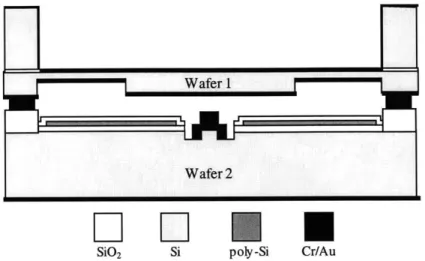
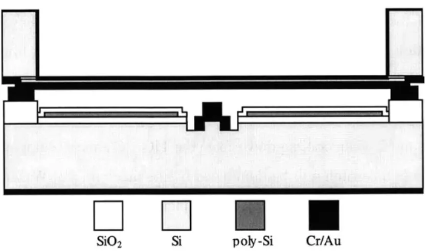
4.2.5 Final Generation Top W afer... 93
4.3 Process Flows...94 4.3.1 Bottom wafer...95 4.3.2 Top wafer ... 98 Silicon diaphragm ... 98 Nitride diaphragm ... 99 4.4 Fabrication Issues...100
4.4.1 Die-level therm ocom pression bond...100
4.4.2 Diesaw ... 101
4.4.3 Gold evaporation...102
4.4.4 M iscellaneous Issues ... 103
Gold agglom eration...103
Stress gradient of diaphragm ... 104
Packaging ... 104
Deep RIE etch non-uniformity...104
4.5 Sum m ary and suggestions...104
Use of wet etchant for diaphragm m icrom achining ... 105
Reduction in device density ... 105
Chapter 5 Testing and Characterization...107
5.1 Introduction...107
5.2 Instrum entation ... 107
5.2.1 W hy dual actuation schem es? ... .. . . .. . . .. . . . .. . . .. . .. . . .. . . . .. . . .. .108
5.2.2 Packaging issues for pneum atic actuation...108
5.2.3 Software ... 111
5.2.4 H ardware ... 111
5.3 Electrical M odel...116
5.4 M echanical M odel...123
5.4.1 D iaphragm deflection profile (Scenario-I)...123
"A pproaching" phase ... 126
"Spreading" phase...129
"Conform ing" phase...132
5.4.2 Pressure-capacitance m odel and discussions (Scenario-I) ... 136
5.4.3 D iaphragm deflection profile (Scenario-II)...139
5.5 Pneum atic Actuation ... 143
5.6 Electrostatic Actuation ... 145
5.7 Com bined Actuation ... 146
5.8 Contact resistance...150
5.9 Switching tim e ... 153
5.9.1 Electrostatic switching ... 154
5.9.2 Pneum atic switching ... 155
5.10 Current capacity ... 157
5.11 Cyclic Operation ... 158
Insulation oxide breakdown ... 159
5.12 Sum m ary ... 161
Chapter 6 Sum m ary, Conclusions, and Suggestions for Future W ork...163
6.1 Sum m ary ... 163
6.2 Conclusions ... 165
6.3 Recom m endations for Future W ork...166
6.3.1 U ltra-high standoff voltage ... 167
6.3.2 Protection arcless-switching circuit...167
6.3.3 Switch cell array...168
6.3.4 Thicker insulation oxide...168
6.3.5 Other design possibilities ... 168
Appendix A D iaphragm buckling ... 171
Appendix B Detailed Process Travelers...173
Appendix C M ask Layouts...191
Appendix D Test fixture design ... 199
Appendix E Poly-silicon surface roughness measurem ent ... 201
Appendix F LabV IEW ® program s ... 203
Appendix G MATLAB* Script for Circular Clamped diaphragms ... 209
LIST OF FIGURES
Figure 1.1 A rcless sw itching schem e... 20
Figure 1.2 Four-by-four switch cell array configuration... 20
Figure 2.1 Typical Paschen curves for hydrogen and air [36]...25
Figure 2.2 V-I plot of two parallel plates (Townsend electrical breakdown mechanism [33])...27
Figure 2.3: The effect of electrode material on breakdown in argon [36]...30
Figure 2.4: Device for Measuring Electrical Breakdown in Narrow Air Gaps...33
Figure 2.5: Process flow for upper and bottom wafers of Breakdown Test Device...33
Figure 2.6: Circuit for measuring electrical breakdown...34
Figure 2.7: Breakdown voltage v.s. Gap separation... 36
Figure 2.8 Charging/breakdown transient curves of different devices: {pedestal #, pedestal diameter, air gap} = (a) {1, 100 pm, 0.5 ptm}, (b)
{1,
100 gm, 1 gm}, (c){19,
200 pm, 1.5 pm }, (d) {19, 200 pm , 1.5 m }. ... 36Figure 3.1 A schematic drawing of a micro electromagnetic actuator...45
Figure 3.2 A schematic drawing of a micro electrostatic actuator...48
Figure 3.3 Typical process flow of bulk-micromachining a diaphragm...52
Figure 3.4 Typical process flow of surface-micromachining a beam...53
Figure 3.5 Drawing of annular diaphragm with central boss ... 55
Figure 3.6 Plot of deflection correction factor due to stress, g, as a function of e [57]. See Equations (3.28) and (3.29). (a) e in linear scale, and (b) e in log scale. ... 59
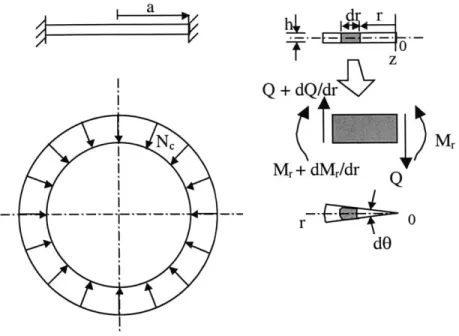
Figure 3.7 Moment equilibrium of a plate element (vertical deflection and slope not shown)...61
Figure 3.8 Diaphragm deflection in a thick-film model...65
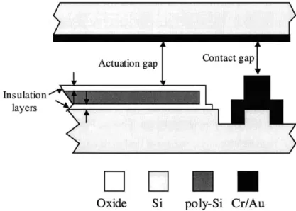
Figure 3.9 Contact gap, actuation gap, and insulation layers of the MEMS switch ... 69
Figure 3.10 Contact areas (apparent, load-bearing, and conducting)...72
Figure 3.11 Asperity-based rough surface model. (a) Geometry model of rough contact surfaces, (b) Elastically deformed asperity (e 5 o)), and (c) Partially plastically deformed asperity (, > w )...7 2 Figure 3.12 Effects of spreading out a-spots on constriction resistance [42]...75
Figure 3.13 Schematic drawing of a circular clamped diaphragm under electrostatic actuation and pneum atic actuation . ... 77
Figure 3.14 M EM S switch design (not to scale)... 80
Figure 3.15 Lumped model for electrostatic actuation: Electrostatic forces (dotted lines) and m echanical force (solid line) vs. gap ... 81
Figure 4.1 First modification on bottom substrate ... 88
Figure 4.2 Second modification on bottom substrate...89
Figure 4.3 MEMS switch design - Generation 1... 90
Figure 4.4 MEMS switch design - Generation 2... 91
Figure 4.5 MEMS switch design - Generation 3... 92
Figure 4.6 Micrograph of a Generation 3 top wafer... 92
Figure 4.7 Latest MEMS switch design -silicon diaphragm... 94
Figure 4.8 Latest MEMS switch design - nitride diaphragm...94
Figure 4.9 Bottom wafer process sequence... 96
Figure 4.10 Micrograph of sixteen i-pedestals in a ring of 300 pm-radius...97
Figure 4.11 Micrograph of a close-up of a 3 pm-pedestal contact...97
Figure 4.12 Top wafer process sequence (silicon diaphragm)...98
Figure 4.13 Top wafer process sequence (nitride diaphragm)...99
Figure 4.14 Crack propagation in overly dried photoresist...102
Figure 5.1 Top view of the test device. Testing window needs to be open and circular diaphragm
needs to be completely sealed after packaging. ... 109
Figure 5.2 Packaging schem e (side view )...109
Figure 5.3 Packaging procedure (perspective view) ... 110
Figure 5.4 Pressure control schem e...112
Figure 5.5 Four-point-probe resistance measurement...113
Figure 5.7 Device cross-section drawing of one single switch cell (electrical model)...116
Figure 5.8 Distributed system circuit model of a single switch cell ... 116
Figure 5.9 Further simplified electrical model of a single switch cell. ... 117
Figure 5.10 Generalized representation of the simplified electrical model...117
Figure 5.11 Electrical model for impedance analyzer: A resistor and a capacitor in parallel...118
Figure 5.12 Low-frequency circuit model of a single switch cell in OFF-state...118
Figure 5.13 Apparent air-gap capacitance Car, gp vs. variable Cai,-gap and apparent resistance R' vs. variable Caigap as computed numerically...119
Figure 5.14 Apparent resistance (R') and apparent capacitance (C'): Measurement data vs. Model sim u latio n ... 12 0 Figure 5.15 Low-frequency circuit model of a single switch cell in ON-state ... 121
Figure 5.16 Discontinuity in capacitance measurement: An indication of change in switch state ... 1 2 2 Figure 5.17 The three proposed phases as diaphragm deflecting downward onto a bottom contact pedestal, (1) "approaching", (2) "spreading", and (3) "conforming". (Scenario-I) ... 125
Figure 5.18 Clamped circular thin plate under uniformly distributed pressure...126
Figure 5.19 Plate deformation profile in "approaching" phase. Each curve represents a 0.05psi pressure in crem en t. ... 12 8 Figure 5.20 Incremental capacitance between deformed plate and ground ... 129
Figure 5.21 Capacitance-pressure curve in "approaching" phase ... 129
Figure 5.22 Dimension definitions in "spreading" phase... 130
Figure 5.23 Plate deformation profile in "spreading" phase...131
Figure 5.24 Capacitance-pressure curve in "spreading" phase (solid line) and "approaching" phase (d ash -dot line)...132
Figure 5.25 Dimension definitions in "conforming" phase...133
Figure 5.26 Plate deformation profile in "conforming" phase. Each curve represents a 0.05psi pressure in crem en t. ... 135
Figure 5.27 Capacitance-pressure curve in "conforming" phase. ... 136
Figure 5.28 Complete capacitance-pressure plot in Scenario-I...137
Figure 5.29 Pressure-capacitance curve comparison: Experimental data (solid lines) vs. Scenario-I m odel (d ash ed line)...137
Figure 5.30 The two phases of diaphragm deflecting downward onto a bottom contact pedestal, (1) "approaching", (2) and "spreading". (Scenario-II)...139
Figure 5.31 Plate deformation in Scenario-Il. "Approaching" phase (dashed): each curve represents 0.05psi increment. "Spreading" phase (solid): each curve represents 50ptm increm ent in touchdow n radius...142
Figure 5.32 Pressure-capacitance curve comparison: Experimental data (solid lines) vs. Scenario-I m od el (d ashed lin e)...14 3 Figure 5.33 Pneum atic actuation test result...144
Figure 5.34 Electrostatic actuation: capacitance vs. actuation voltage ... 145
Figure 5.35 Actuation current of the switch...146
Figure 5.36 E lectrostatic test result...146
Figure 5.37 Combined actuation: Simulated Vp,u- (squares) vs. measured Vp,1u- (diamonds)... 148 Figure 5.38 Pneumatic pressure, electrostatic pressure, and total pressure under combined a c tu a tio n ... 14 9
Figure 5.39 Resistance measurements of a device with insufficient metal height...150
Figure 5.40 Contact resistance vs. pressure ... 152
Figure 5.41 Contact resistance vs. current (positive current flows from bottom to top)...153
Figure 5.42 Hardware setup for switching time test ... 154
Figure 5.43 Switching time (device switching electrostatically) ... 155
Figure 5.44 Switching time (device switching pneumatically)...156
Figure 5.45 Current capacity for one single switch cell...157
Figure 5.46 C ontact resistance vs. cycles...158
Figure 5.47 First 30 cycles in cyclic operation test...159
Figure 5.48 Insulation oxide breakdown test (350'C, 2min. thermal treatment)...160
Figure 5.49 Insulation oxide breakdown test (no thermal treatment) ... 160
Figure 6.1 Other MEMS switch design: A vertically-moving structure deflects down and electrically connects with two pedestal contacts...168
Figure A. 1 Buckling of thin bossed silicon diaphragms...171
Figure A.2 Buckling of thin bossed silicon diaphragms coated with nitride film...172
Figure C .1 M ask ID : B TM -N I...191
Figure C .2 M ask ID : BTM -N D ... 192 Figure C .3 M ask ID : BTM -N B ... 193 Figure C.4 M ask ID : B TM -N G ... 194 Figure C.5 M ask ID : BTM -N M ... 195 Figure C .6 M ask ID : TO P-N B ... 196 Figure C .7 M ask ID : TO P-N M ... 197
Figure C.8 Mask ID: TOP-NI...198
Figure D. 1 Drawing for the sealing fixture design...199
Figure D.2 Drawing for the alignment jig design...200
Figure E. 1 Surface condition of bottom substrate (measured by WYKO surface profiler)...201
Figure E.2 Surface roughness of the toE surface on poly-silicon actuation electrode...202
Figure F. 1 Front panel of a LabVIEW program used for device characterization while sweeping actuation voltage at biased pressures...203
Figure F.2 Block diaphragm of the LabVIEW® program shown in Figure F. 1. (1 of 5)... 204
Figure F.3 Block diaphragm of the LabVIEW® program shown in Figure F. 1. (2 of 5)...205
Figure F.4 Block diaphragm of the LabVIEW® program shown in Figure F. 1. (3 of 5)...206
Figure F.5 Block diaphragm of the LabVIEW* program shown in Figure F. 1. (4 of 5)...207
LIST OF TABLES
Table 1.1 Advantages of switching devices: Solid-state transistor vs. Electromagnetic relays...17
Table 1.2 Specification requirements of switching devices: Signal switching vs. Power switching ... 1 7 Table 1.3 Selected micro switching devices published recently ... 18
Table 1.4 Summary on device performance...21
Table 2.1: Breakdown voltage measurements... 35
T able 3.1 G old properties...83
Table 3.2 Derivation of constriction resistance... 84
Table 3.3 Design and target specifications... 86
Table 4.1 Comparison of anisotropic silicon etchant systems ... 105
Chapter
1 INTRODUCTION
This thesis presents a MEMS electrostatic actuator for power switching applications. This normally-open SPST2
switch prototype employs a vertically moving bulk-micromachined diaphragm structure, features metal-to-metal electrical contact, and can be alternatively actuated with pneumatic pressure. The underlying physics in key aspects of a power switch are investigated and the results are used as general design guidelines for the MEMS switch. The design theories are realized through fabricated devices with good agreement between the theory prediction and the experimental data. Our design of a MEMS power switch employs a two-wafer stack structure with a clamped circular diaphragm as the moving structure. This hockey-puck power paradigm also possesses favorable features such as good heat dissipation and easy
packaging.
Section 1.1 contains the historic background of micro switching devices, the device attributes, and applications. In Section 1.2, other micro switch/relay works published recently are surveyed and listed in for a side-by-side comparison. Section 1.3 briefly describes the project motivation and goal. In Section 1.4, a system viewpoint is provided to explain why SPST switch cell under cold-switching scenario will be considered in the thesis. Finally, Section 1.5 outlines the framework structure of the thesis.
1.1 Background
Relays and switches are often regarded as interchangeable terms for electromechanical devices that alternate, under a controlled fashion, between two (sometimes more) configurations of electrical connections. Generally, a relay is a four-terminal device having two isolated ports. A pair of the terminals, or port, is powered to control the state of the device. The other port makes
1 Micro-Electro-Mechanical Systems
or breaks its connectivity, depending on the state of the device. Therefore, it is possible to control high power flows using a relay driven by relatively low actuation power. The most commonly seen relays are magnetically driven and the simplest magnetic relay consists of an electromagnet, an armature, a mechanical spring, and a set of electrical contacts.
In other switching devices, one of the control terminals and one of the line terminals share a common electrical potential and merge into one, and the three-terminal switching device is conventionally called a switch. The first appearance of an electronic device of this kind in history dates back in early twentieth century when the audion (triode) was invented [1]. The audion was encapsulated in a vacuum and made up of a heated wire (the filament) that emitted electrons, a closely separated metallic plate, and a third electrode (the grid) inserted in between the filament cathode and the plate. The grid voltage controls the charge flow between plate and cathode. The invention of such grid-controlled vacuum-tube rectifiers marked the dawn of the vacuum tube era spanning over the first half of the twentieth century. Bipolar and field-effect semiconductor switching devices, which operate without heatedfilaments and do not need to reside in a vacuum, were invented in the 1940-50's and soon gained popularity to open the transistor era that lasts to date. The initial applications of the electronic devices were to telephone and radio communication. Nowadays, information processing and signal transmission remain the dominant applications of electronics but the technological breakthroughs have also benefited power engineering whose major concerns are power processing and power transmission. Basic semiconductor power switching devices include diodes (bipolar and Schottky), transistors (BJT3 and MOSFET4), and thyristors5 [2] [3]. The success of microelectronics is empowered by the advancements of semiconductor fabrication technologies that continuingly make possible smaller and better devices. Silicon, the most popular semiconductor material and probably the most exhaustively studied material on Earth, with the availability of a complete machining tool set for selective material addition/subtraction and planar pattern definition on a substrate on a greatly reduced yet precise dimension scale, has made itself a legitimate structural material for micro-machines [4]. Similar to what miniaturization of silicon electronic devices has brought to the world, silicon micro-machines can lead to technological revolutions of unprecedented magnitude. Such micro-machines are often referred to as MEMS devices.
3 Bipolar .unction Transistor
4 Metal-Oxide-Semiconductor Field-Effect Transistor
Solid-state transistors and conventional electromagnetic relays have been extensively used in various industrial applications as switching devices to make or break circuits. The advantages of each type of the switching devices are listed in Table 1.1.
Solid state transistors Magnetic relays
Small size Low on-state resistance
Mass Producibility High off-state blocking voltage Easy on-chip integration High current capacity
Fast switching speed Good control/signal isolation Low actuation power
Table 1.1 Advantages of switching devices: Solid-state transistor vs. Electromagnetic relays
The choice of one type of switching device over the other depends on application-specific requirements. The two most prevalent applications of the switching devices are signal routing and power routing. In addition to common requirements, such as long lifecycle, robust operation, high open-contact and control-to-contact breakdown voltages, and minimal bouncing effects, etc., the two major applications of the switching devices, signal and power redirectioning, also call for fairly distinct specifications on the switches as illustrated in Table 1.2.
Signal switching (High-fidelity) Power switching (High-efficiency) Low insertion loss Low on-state voltage drop
Wide frequency bandwidth High current capacity
Low signal cross-talk Low off-state leakage current
Low parasitic impedance
-Table 1.2 Specification requirements of switching devices: Signal switching vs. Power switching
1.2 Other Micro Relays/Switches
The emergence of MEMS technologies has brought global attention to the possibility of merging conventional macroscopic relay attributes with MEMS device attributes into a new family of switching devices: MEMS based relays/switches. One of the earliest MEMS devices is an electrostatic switch developed two decades ago [5]. Electrostatic actuation remains the most popular actuation scheme, but other methods of actuation have also been broadly investigated. Most MEMS relay/switch studies found in the literature either focus on signal switching applications, such as automatic test equipment [6-10], telecommunications [11-18], and logic
operation [19], or are oriented toward technology demonstration [5, 20-25]. Few [26] have addressed the need for a MEMS-based relay/switch tailored for power applications, and that is the gap this thesis is trying to fill. In Table 1.3, a selected collection of recent publications on micro switches/relays is illustrated. Cronos Integrated Microsystems Inc.6 has unveiled a thermally actuated micro relay as the company's first commercial product. However, not much device detail has been revealed to the public so far.
Year Organization Actuation Act Pwr/Volts Contact Current Speed Application Cycles Ref.
1979 IBM Electric - 5 Q - 40 ts AC signal - [5]
1994 Neuchatel Electric 50-75V - - 4 js Signal le9 [27]
1995 EG&G Electric 50-100 V 3 Q - 20 ps ATE le8 [6]
1995 NTT TCMA' >300mA 3 Q - loms -_- [21]
1995 CWRU Electric 35-150V <20Q 150mA 5-40kHz - - [23]
1995 Rockwell Electric 28V, 1.4uW 0.22Q 200mA 30 ps Telecomm. - [12]
1996 TI Electric 50-300V - - -8s Microwave - [28]
1997 Omron Thermal 27V, 25mA - - - 1-- [29]
1997 GA Tech Magnetic 180mA,33mW 2-3Q 2 1.2A 1-5ms Automotive 3e5 [30]
1997 NEU Electric 30-400V 50mQ 5mA - ATE le9 [7]
1998 CSEM Magnetic 8mA, 14mW 0.42 - 0.2-0.3ms Signal >1.5e7l[8]
1998 UCLA Electric 35V lkQ 10mA 4 Hz - - [25]
1998 NJIT Thermal 12mW + 10mW 2.1-35.6Q - 0.1-0.5ms Signal le5 [31]
1999 NTT Electric 15V 5Q - 10kHz Signal - [19]
1999 CSEM Magnetic 2V, 16mW 0.4Q - ims Signal 1e7 [10]
Table 1.3 Selected micro switching devices published recently 1 Thermally Controlled Magnetization Actuation
2 Minimum resistance measurement: 0.85Q
3 Resistance measurement made with manual contact closure.
1.3 Power MEMS Switches: Motivation and Goal
One of the promising high power applications of MEMS switches is automotive relay replacement. Fifteen million automobiles are manufactured per year in the U.S. and an average car uses approximately 15 relays which is increasing rapidly to as many as 50 per car. This puts the automotive relay market at 225 million relays per year in the U.S. alone. Thus, one important target application for a MEMS switch would be in the replacement of the conventional relay block in an automobile. The intent there is to embed MEMS switches at the point of use instead of running wire harnesses across the engine compartment to a relay block. Embedding relays at
the point of use reduces car weight and power line loss, and improves fuel economy and automobile performance. Another equally promising market for the power MEMS switch is application in residential circuit breakers.
The goal of this thesis is the development of a MEMS switching device for automotive, residential, and/or other power distribution applications. The power MEMS switching device should possess the key attributes of a power switch, such as high current-carrying capacity and low on-state resistance for efficient power transmission with low loss. Unlike signal switches that need to deliver/receive information with high data transmission rate and high fidelity, requirements on switching speed, on-state insertion loss, off-state parasitic capacitive coupling, signal cross-talking noises, and so on are not major issues for the power switches to be studied in this thesis. As with signal switches, the power MEMS switches call for high off-state resistance and high standoff voltage.
1.4 System Viewpoint
It is believed that the lifetime of the mechanically moving MEMS switch is dictated more by the wear of its contacts than by the failure of the moving member itself. Since arcing is a well-known cause of contact wear, we propose a protective circuit to parallel the power MEMS switch device as described in Section 1.4.1. This scheme enables us to focus on cold switching in the study of the MEMS power switch behavior. Moreover, to scale up the current capacity and to facilitate different switch configurations with SPST switch cells at the packaging level, Section 1.4.2 proposes a four-by-four switch cell array design.
1.4.1 Arcless Switching Scheme
The protective switching scheme is shown in Figure 1.1 where the MEMS switch is paralleled with a solid-state-transistor based circuit and the circuit turns on before and turns off after the MEMS switch. In this way, the contacts of the MEMS switch are protected from being brought into close vicinity with a high potential difference across them thereby preventing arcing due to hot switching. Moreover, any inductive energy stored behind the switch is dissipated by the protective circuit thereby protecting the thermally vulnerable switch contacts. This protective circuit can be incorporated with the MEMS switches via on-chip integration or off-chip packaging and will be the subject of future investigation.
Protective Circuit MEMS Switch tn mn On -IDEff time 1
Figure 1.1 Arcless switching scheme
1.4.2 Switch Cell Array Configuration
The purpose of the switch cell array design is two-fold: in addition to the apparent current capacity boost, such switch cell arraying permits a simple SPST switch cell design and leaves more complicated switch configurations to packaging-level connections. Furthermore, if the protective/control circuit mentioned in Section 1.4.1 is to be implemented off chip, it can realized by replacing one of the cells in the array with a circuit cell. Figure 1.2 shows the cell array
schematically.
Figure 1.2 Four-by-four switch cell array configuration
1.4.3 Quick Summary on Device Performance
To put the device in perspective with other micro relay/switch work, and with the power switch requirements discussed earlier, this section tabulates in Table 1.4 an upfront summary of the performance of the power MEMS switch investigated in the thesis. This device exhibits on-state characteristics among the best of its kind and, more significantly, the current capacity per cell appears promising for power applications.
Actuation Scheme Electrostatic Zero actuation power during steady state. Actuation Voltage Turn-on: 20 V Turn-off: 14 V Lowest turn-on voltage: 15 V.
Mechanical Design 2.4-mm diameter diaphragm Good heat dissipation.
One Switch
Rcontact Generally < 50 mQ Lowest resistance: 14 mQ.
Current Capacity 400mA Current/actuator area: 90 mA/mm
2 . With 4x4 array design: > 6 A.
Vbreakdown > 300 V Sufficiently high for automotive applications.
tswitch Turn-on: 5 ms Limited by squeeze-film damping; can Turn-off: 20 ms be improved.
Not much performance degradation
Cyclic Operation > 4000 operations oserved.
observed.
Table 1.4 Summary on device performance
1.5 Thesis Overview
The remainder of the thesis is organized as follows. Chapter 2 investigates theories and experimental results of electrical breakdown in narrow air gaps. This work establishes guidelines for the MEMS switch design Chapter 3 analyzes various switch designs and settles on a promising candidate design. Chapter 4 addresses the fabrication techniques of different device generations and their behavior. Chapter 5 discusses various device performance characterizations, how tests are implemented, and their results. Finally, a summary, conclusions, and suggestions for future work are given in Chapter 6.
Chapter 2
ELECTRICAL BREAKDOWN IN
NARROW AIR
GAPS
2.1 Introduction
This chapter focuses on two main subjects. First, the underlying physics of electrical breakdown phenomena in micron-scale air gaps are summarized. Second, an empirical study of the standoff
voltages achievable in such narrow air gaps is presented. Acquiring the knowledge of electrical breakdown through experimental results on actual devices, along with the experience gained in the course of design, fabrication, and experimentation of breakdown test devices is an important step toward the design of actual MEMS switches. Therefore, an investigation of electrical breakdown in narrow air gaps is chosen to be the first challenge of this thesis.
Various factors must be taken into account in an in-depth study of the electrical breakdown in gases. They include gas pressure, gas temperature, gap spacing between electrodes, electrode shape, electrode surface condition, material of electrodes, composition of the gas, radiation in the space, and uniformity of electrical field. The atomic, molecular, electronic, ionic, and photon collision processes in the gas and at the electrodes, which can be involved in the various mechanisms of breakdown, are themselves of fundamental physical interest. A full-scale study of electrical breakdown in micron-scale gaps can make up a doctoral thesis in fundamental physics in its own right and is impossible to carry out here. Our simplified experimental approach will consider only gap separation and contact patterns as variables. Also, issues such as how fast gases respond to the electrical field and break down, and how fast gases recover from a heavy current carrying state back to their original insulating state after an applied potential is removed are not addressed in this thesis.
In what follows, Section 2.2 develops a basic understanding of the electrical breakdown in air gaps from our everyday observations and some existing theories of electrical breakdown found in
the literature such as [32-35] are discussed. These references are good introductory reading for
readers interested in much more detail than can be presented here. Section 2.3 comments on the electrical breakdown theories especially in the case of very narrow air gaps. Section 2.4 discusses the fabrication of breakdown test devices employed here, the test hardware as well as the test results. Lastly, Section 2.5 concludes what we learn from the electrical breakdown test and presents the author's suggestions for further studies in improving the breakdown strength of
MEMS devices.
2.2
Electrical Breakdown in Gases
Our perception of gas has always been a nearly perfect insulator and it is generally true in our everyday life experience. Under certain conditions, however, when an electric field of sufficient intensity is applied across two electrodes, the gas could suddenly become relatively conductive. The transition from insulating to conducting states is a physical change often referred as the electrical breakdown of the gas. This transitional process occurs in very short times varying from milliseconds to nanoseconds.
The most commonly seen occurrences of electrical breakdown are lightning, fluorescent lamps, and sparks between hands and doorknobs in dry winter days. Electrical breakdown in gases is a very involved phenomenon and, in general, requires electron avalanche. It has to do with a sudden and dramatic change of gas dielectric property as the collision of sufficiently high-energy particles ionizes material molecules and produces a large number of free current carriers. To achieve a self-sustaining discharge, any ionization on average must produce some means for at least one new ionization to occur. The condition under which such transition takes place is a function of a variety of parameters as briefly described in Section 2.1. The following section will describe the typical process of electrical breakdown and provide an introduction to electrical breakdown theories.
Scientists have studied the electrical breakdown of gases for over a hundred years in order to answer two main questions. Firstly, is it possible to explain and to predict, from our understanding of collision processes, the lowest voltage at which electrical breakdown will occur for a given set of electrodes at a given gap separation in a given gas at a given pressure? In other words, is it possible to elucidate a mechanism of breakdown and derive a criterion for the breakdown voltage? Secondly, is it possible to establish a theoretical explanation, based on collision processes, to account for the breakdown process from the first few electrons that must always be present to initiate breakdown to the final form of the discharge? The following sections
will describe, in a very simplified way, the breakdown phenomenon and summarize the generally accepted theories that have been established to answer these questions.
2.2.1 Paschen's Law
As mentioned earlier, there are various factors that must be taken into account in studying the breakdown in gases, such as gas temperature, gas pressure, the shape, surface condition, and material of electrodes, the gap spacing between electrodes, the composition of the gas, radiation, and the uniformity of the electrical field. An empirical criterion found by Paschen in 1889 [32] states that over a certain pressure and temperature range in a static uniform field, using parallel plate electrodes, the breakdown voltage of a gas depends on the product of gas pressure and gap separation. Thus,
V, =
f'(pd)
(2.1)where V, is the sparking potential, or breakdown voltage, p is the gas pressure at a given temperature, d is the gap spacing, and
f
is a function of pd only. This criterion has been shown to hold for a wide range of conditions up to a pressure of about 150 psi and is now known as Paschen's Law. Sometimes, Paschen's Law is also stated asV, =
f(Nd)
(2.2)where N is the gas density in molecule number per unit volume. This latter form of the law is useful when considering a sealed system where pressure increases with temperature but N remains constant, so the breakdown strength remains unchanged. The breakdown voltages for gases decrease as the product of p and d is reduced, and reach a minimum at a value of pd on the order of 1 to 10mm-Hg x cm [34, 35]. 112 1600 Air 1200-a' 800--400 -.0 4 8 12 16 20 24 28 pd (rnm-torr)
At present, two fundamental breakdown mechanisms have been established to account for this relationship. The first is a relatively slow mechanism, which needs a large number of generations to produce breakdown. This is referred to as the Generation Mechanism or Townsend Mechanism. The second is a rapid mechanism, which develops directly from the first avalanche to breakdown. This is referred to as the Streamer Mechanism or Kanalaufbau. There also exist variations of these mechanisms, which can be understood as transitions between them. These two mechanisms are briefly discussed next.
2.2.2
Townsend Mechanism
Townsend's paper in 1910 [33] illustrates this theory by examining the current between parallel plate electrodes under increasing electric force; see Figure 2.2. As the electric field increases, the leakage current between the plates first increases accordingly. This leakage current very quickly saturates at a certain value, Io. After that, any further potential increase does not change the leakage current very much over a wide range of electric potential. As electric potential is increased still further, the rate of leakage current increase suddenly jumps to an appreciable value. Townsend explains this as follows. Under low electric field, a dielectric gas is in its normal state and electrically non-conductive because there is no significant number of free electrons or ions to carry electrical current between the electrodes. However, there is always a small number of low-energy charged particles present in the gas due to environmental radioactivity and cosmic radiation. This limited amount of free electrons accounts for the leakage current, Io, at low electric field. A single free electron could ionize a gas molecule by collision, producing two free electrons and a positive ion. The higher the electric field intensity, the more electrons colliding with ions which generates more charge particles. This cumulative process eventually produces a swarm of free electrons and ions, generally called "electron avalanche", the gas then becomes conductive. Secondary avalanches may be produced at the cathode by the impact of positive ions or photons from an ongoing avalanche. This in turn initiates more avalanches, creating a self-sustaining discharge. This electrical breakdown model is known as the Townsend theory of breakdown.
Cbrent+ /
ji
b
aa
Voltage
0 V
Figure 2.2 V-I plot of two parallel plates (Townsend electrical breakdown mechanism [33])
Townsend's theory of breakdown is good for low pd, between 200 torr-cm and 1000 torr-cm [37], where p is the gas pressure between the parallel plates and d is their separation distance. Townsend also develops the following formula and finds good agreement with experimental data.
__ io _ (2.3)
1- y(em -1)
where io is the saturated leakage current, a is the so-called first Townsend multiplication coefficient, and y is the so-called second Townsend ionization coefficient. Physically, the first Townsend coefficient, a, indicates the number of new electrons created by a traveling electron through a path of length 1 cm. It is concerned with the electron multiplication by primary ionization. The second Townsend coefficient, y, is also called the generalized secondary ionization coefficient and represents the efficiency of production of secondary electrons per ion pair formed in the gas. Breakdown then occurs when the denominator becomes zero, or
-1 = e -1 (2.4)
References [33-35] provide a more thorough understanding of Townsend's description of gas breakdown phenomena.
2.2.3 Streamer Mechanism
There exists another breakdown mechanism that progresses much faster than the Townsend Mechanism described in the preceding section. The most striking differences of this mechanism compared with the Townsend breakdown mechanism are as follows.
1. There is no cathode or gas secondary ionization process as in a Townsend type breakdown mechanism, thus the breakdown potential is independent of the nature of the cathode surface. Additionally, photons from the avalanche head produce free electrons by photo-ionization.
2. High field distortion, due to space charge at the avalanche head, moves the free electrons toward the avalanche head and generates further cumulative avalanches. When the space charge suddenly distorts the field, breakdown suddenly occurs. The criterion that sets the value of breakdown potential is uniquely determined by space-charge distortion of the electric field.
3. It is feasible that breakdown could take place in a very short time, less than 0.1 us for a 1 cm gap, and that luminous streamers can cross the gap in less than an electron transit time.
The Streamer theory applies when the number of electrons in the average avalanche reaches a critical value, generally taken as 108. The transition from a Townsend mechanism, which operates at the lower pd values, to a Streamer mechanism takes place when pd > 200 torr-cm, where p is the gas pressure between the parallel plate electrodes and d their gap separation distance.
In conventional relays or MEMS switches/relays, the open contact separation ranges from millimeters down to micrometers, and the product of gas pressure and electrode separation (pd), is normally well below 200 torr-cm. Therefore, the Streamer mechanism does not apply in such small air gaps. Readers with more interest in Streamer breakdown mechanism should refer to [34, 35] for further discussion.
2.2.4 Summary of Breakdown Theories
In essence, electrical breakdown can be seen as a competition between the recombin-ation/absorption rate and the generation/multiplication rate of such free electrons and ions. When the former dominates, the gas is nonconductive; when the latter dominates, electrical breakdown occurs. The experimental data of electrical breakdown found in the literature affirm Paschen's criterion, which is now well accepted and referred to as Paschen's Law, Equation (2.1) or (2.2).
Paschen's Law says that the dependencies of breakdown potential between parallel plates on pressure (p) and on gap-distance (d) are linearly linked with each other and appear as their product (pd).
Two breakdown models are established to explain the fundamental physics of Paschen's Law in different pd ranges: the Townsend breakdown model for the lower pd range, and the Streamer breakdown model for the higher pd range. Secondary ionization at the cathode plays an important role in the Townsend breakdown mechanism, as the positive ions and photons colliding with the cathode provides the self-sustaining discharge. Therefore this breakdown phenomenon is more dependent on the characteristics of the cathode. In the Streamer breakdown theory, local electron avalanche causes photo-ionization and field distortion by space charge, driving free electrons toward the avalanche head and initiating more avalanche, more photo-ionization, more field distortion, and more free electrons into the cloud. The gas can respond to an electric field in a very short time and spark under streamer breakdown model.
The transition from a lower pd-valued Townsend breakdown mechanism to a higher pd-valued Streamer breakdown mechanism takes place when pd ~ 200 torr-cm. If we fix the air pressure at atmospheric pressure, p = 760 torr, Townsend breakdown theory is applicable to cases with electrode separated less than 2.6 mm. Generally, the off-state contact separation, d, is orders of magnitude less than 2.6mm for MEMS-based devices. From this point of view, the Townsend breakdown mechanism seems to be a more appropriate model to explain the breakdown process in MEMS relay/switch applications at atmospheric pressure due to the small gap separation in
MEMS devices.
2.3 Discussion of Electrical Breakdown in Narrow Air Gaps
The limits of Paschen's law in terms of pd ranges is still an open question. However, with the assumption that Paschen's law applies well into very-low pd realm, it is possible to investigate electrical breakdown in narrow air gaps by examining into Paschen's curves in the ultra-low pd range. Under this assumption, the data in the low pd regime of the Paschen curves, which are taken in vacuum pressures, can be employed to predict the electrical breakdown in very narrow air gaps at atmospheric pressure. This is the reason why the experimental data for electrical breakdown voltages in the ultra-low pd ranges found in the literature were primarily obtained with gap separations in the centimeter range and air pressure brought down in the vacuum range. In other words, low pd values were achieved by pumping the air pressure down to the m-torr range while keeping the electrode separation fixed at a fair distance [35]. This is understandable
since well-developed vacuum technology makes it more manageable to pump down and control pressures at vacuum levels than to bring two exceptionally planar polished electrodes into very close proximity while maintaining uniform and precise gap separation in micron range.
Figure 2.1 in Section 2.2.1 shows typical Paschen curves of hydrogen and air. If the curve for air in this figure is chosen to study the breakdown of air in narrow gaps, it can be seen that the breakdown voltage for air decreases as pd is reduced, reaching a minimum of 360 V at pd = 5 torr-mm, and then increases. This means that, other conditions being the same, the minimum breakdown voltage of air at 760 torr atmospheric pressure, should take place at 360 V when the electrodes are 6.6 pm apart. Note that the field emission of electrons limits the electric field to about 10 9 V/m or lower. The breakdown voltage should rise with either closer or wider gap spacing.
Before examining whether Paschen's law provides a good prediction of the breakdown voltage of the micrometer-scale air gaps in MEMS-based devices, consider the following issues.
(1) Surface roughness
Figure 2.3 shows another plot of breakdown voltage curves with different electrode materials. It can be seen that a variation of breakdown voltage occurs with different types of electrode materials as pd reduces. This is not surprising since secondary cathode ionization is a significant mechanism in Townsend breakdown theory, which is the predominant breakdown model in the low pd regime. The lower the pd value, the more important role the electrode surface plays in the electrical breakdown mechanism. At higher pd, surface condition has negligible effect.
3000 1000 300 100 Na S 3 10 30 100 pd (torr x cm)
Remember that the data in the low pd range were obtained with experiments in vacuum pressure and with relatively large gap separations. Surface roughness of electrodes, which might not be of importance at such considerable gap distance, can now become a even more important factor in the case of very narrow separation at atmospheric pressures. In other words, a higher dependency of breakdown voltage of air at atmospheric pressure on the electrode conditions in very narrow gap separation should be expected, especially surface roughness. A uniform electric field might no longer be a valid assumption. This is important because locally distorted fields due to surface roughness can enhance ionization, and pointed protrusions can support electron emission. These surface roughness effects can be of importance in the electrical breakdown between very closely separated electrodes.
(2) Collision number
The collision count that an ion or electron will encounter traveling across a voltage-biased gap is linearly proportional to the length of travel (gap spacing) as well as the collision probability along the travel (air density or pressure). Since the atomic, molecular, electronic, ionic, and photon collision processes in the gas are crucial physical events that lead to eventual electrical breakdown, it can be argued that one rationale behind Paschen's law, Equation (2.1) or Equation (2.2), is that the electrical breakdown voltage across two parallel electrodes is a function of total particle collision number along the gap. Therefore, to first order approximation, a constant product of travel length (d) and collision probability (p) dictates a certain number of collisions a particle would see crossing the
gap.
From the discussion of surface roughness, it has been argued that the surface condition of electrodes can be of greater consequence for narrower gap separation. This follows from the secondary ionization at the cathode as proposed by Townsend [33]. The frequency of particle collisions at the cathode electrode is still a linear function of air density or pressure, but its dependency on gap spacing, if any, is very weak. In other words, Paschen's criterion relates the breakdown potential of air with particle collision counts within the electrodes, which is a function of pd; however, as gap separation gets closer, collisions at the electrode, which is a function of only pressure (p) but not gap distance (d), plays a more important role. Therefore it would be reasonable to expect more deviation from predictions based on Paschen's law for narrower gap separations.
![Figure 2.2 V-I plot of two parallel plates (Townsend electrical breakdown mechanism [33])](https://thumb-eu.123doks.com/thumbv2/123doknet/13985728.454605/27.918.230.682.113.419/figure-plot-parallel-plates-townsend-electrical-breakdown-mechanism.webp)
![Figure 3.6 Plot of deflection correction factor due to stress, g, as a function of 2 [57]](https://thumb-eu.123doks.com/thumbv2/123doknet/13985728.454605/59.918.192.707.122.368/figure-plot-deflection-correction-factor-stress-g-function.webp)