advances.sciencemag.org/cgi/content/full/6/1/eaav7523/DC1
Supplementary Materials for
An electrically pumped surface-emitting semiconductor green laser
Yong-Ho Ra, Roksana Tonny Rashid, Xianhe Liu, Sharif Md. Sadaf, Kishwar Mashooq, Zetian Mi**Corresponding author. Email: [email protected] Published 3 January 2020, Sci. Adv. 6, eaav7523 (2020)
DOI: 10.1126/sciadv.aav7523
The PDF file includes:
Text S1. Simulation for photon confinement in the vertical direction Text S2. Nanohole patterned Ti mask substrate for selective area epitaxy Text S3. Epitaxial growth of InGaN/AlGaN core-shell heterostructures Text S4. TEM specimen preparation using a focused ion beam system Text S5. Ga-polar n-GaN nanocrystal structure
Text S6. Projection effect image and quasi-3D structure of InGaN/AlGaN quantum disk layers Text S7. Properties of semipolar InGaN/AlGaN core-shell heterostructures
Text S8. NCSEL device fabrication
Text S9. Electroluminescence measurement Text S10. Calculation of far-field radiation pattern Text S11. Measurement of far-field radiation pattern
Text S12. Polarization measurement of the light emission of InGaN NCSELs
Fig. S1. Variation of the effective refractive index along the growth direction and the TM polarized mode intensity profile.
Fig. S2. Schematic illustration and field-emission SEM image of the patterned Ti thin-film nanohole mask fabricated on n-type GaN template substrate.
Fig. S3. TEM lamella preparation of the nanocrystal. Fig. S4. Ga-polar n-GaN nanocrystal structure. Fig. S5. Projection effect in quasi-3D structure.
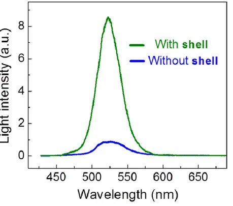
Fig. S6. PL emission spectra of InGaN/AlGaN core-shell multiquantum disk nanocrystals (green curve) and InGaN/GaN multiquantum disk nanocrystals without AlGaN shell (blue curve) measured at 300 K.
Fig. S7. Schematic illustration of the full device fabrication, including passivation, planarization, photolithography, and contact metallization techniques.
Fig. S8. Schematic illustration of the measurement setup for electroluminescence spectra. Fig. S9. Schematic illustration of the far-field measurement setup with a CCD camera at a distance above the NCSEL device.
Fig. S10. Schematic illustration of the polarization angle measurement. References (69–83)
Text S1. Simulation for photon confinement in the vertical direction.
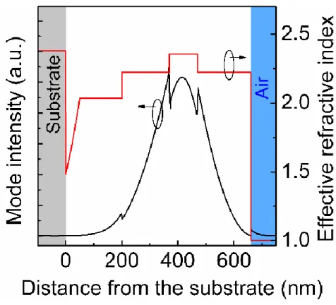
Due to larger refractive index for InGaN compared to GaN, the effective refractive index is higher around the active region. In order to calculate the effective refractive index, the nanocrystals are assumed to have flat top morphology. The lattice constant is 250 nm and the spacing between nanocrystals is 30 nm. The refractive index is 1.75 for the filling material (polyimide), 2.69 for InGaN, 2.35 for AlGaN, and 2.38 for n-GaN and p-GaN (69-72). The diameter at root of the nanocrystals is approximated to grow from 170 nm to 255 nm within a height of 50 nm. Due to the high viscosity of the filling material and small spacing between nanocrystals, air gaps exist near the root of GaN nanocrystals. Considering the lengths of the segments in Fig. 1A in the main text, the variation of effective refractive index in the vertical direction and the corresponding TM polarized mode are calculated as shown in fig. S1. It is observed that the mode is mostly confined near the active region due to higher refractive index.
Fig. S1. Variation of the effective refractive index along the growth direction and the TM polarized mode intensity profile.
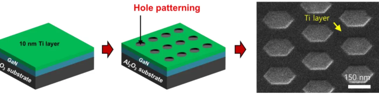
Text S2. Nanohole patterned Ti mask substrate for selective area epitaxy.
Nano-hole masks for the selective area growth (SAG) were fabricated on n-type GaN (4 µm thick) template on Al2O3 (0001) substrate. Firstly, a 10 nm thin Ti layer was deposited by
e-beam evaporator system. A positive Poly(methyl methacrylate) (PMMA) was used as a resist layer with spin-coating technique. The e-beam lithography process was optimized to obtain uniform arrays of nano-holes with a diameter of ~180 nm and a lattice constant of 250 nm in triangular lattices. The lateral growth effect was taken into account in the pattern design. Subsequently, a MIBK:IPA (1:3) solution was used for development process. Thereafter, the exposed Ti thin film area was etched down by reactive ion dry-etching technique using CF4/O2 plasma gas. The nano-hole patterned substrate was cleaned by Hydrogen Chloride
acid (37%) prior to loading into the MBE growth chamber. Prior to the GaN nanocrystal SAG, a nitridation step was performed at 400 °C with a plasma power of 380 W and a nitrogen flow rate of 1 sccm. Consequently, the thin Ti film was converted to TiN film which prevents the formation of cracks and degradation at elevated temperature. Fig. S2 shows the FE-SEM image of the patterned hexagonal shape Ti mask with an opening hole size of ∼180 nm.
Fig. S2. Schematic illustration and field-emission SEM image of the patterned Ti thin-film nanohole mask fabricated on n-type GaN template substrate.
Text S3. Epitaxial growth of InGaN/AlGaN core-shell heterostructures.
The InGaN/AlGaN core-shell heterostructures were incorporated in the laser active region. First, the core InGaN disk layer was grown on the top surface region of n-GaN nanocrystal. Due to the strain induced self-organization effect, the size of the InGaN disk becomes smaller than the n-GaN nanocrystal diameter. The incorporation of AlGaN barrier layers, instead of GaN barrier layers, leads to the formation of an AlGaN shell structure surrounding the InGaN quantum disk active region, due to the smaller Al adatom diffusion length compared to Ga and In adatom diffusion (73). As a consequence, the growth fronts including the top and sidewalls of the InGaN region can be covered by AlGaN layers, thereby leading to the spontaneous formation of large band-gap AlGaN shell structures (54, 74). The growth
conditions of InGaN/AlGaN multiple quantum disk layers included a substrate temperature of 650°C, a nitrogen flow rate of 1.2 sccm, a forward plasma power of ~ 350 W, In BEP ~8.1 × 10⁻⁸ Torr, Ga BEP ~1.8 × 10⁻⁸ Torr, and Al BEP ~4.2 × 10⁻⁹ Torr, respectively. By repeating the growth process, coaxially aligned cone-like AlGaN shell layers can be fabricated
Text S4. TEM specimen preparation using a focused ion beam system.
The cross-sectional TEM sample preparation was performed in a FIB instrument (FEI Helios Nanolab 660 DualBeam) incorporating a gallium (Ga) liquid metal ion source and in-situ scanning electron microscopy imaging using a field emission source. The preparation of TEM lamella by the FIB lift-out technique was carried out as follows: a thick Cu layer was firstly deposited on the substrate to protect the top surface of the nanocrystals. Thereafter, the milling for lamella was processed to remove only regions A and B of the hexagonal shape nanocrystal as shown in fig. S3A, and after milling the GaN lamella has <100 nm thickness. Lastly, the cross-sectional surfaces of lamella were cleaned in low voltage mode by FIB to remove the beam damage and contamination layers. For the TEM measurement, the a-plane (21̅1̅0) zone-axis orientation of TEM lamella was used to observe the InGaN/AlGaN multi-quantum disk layers in the active region, shown in fig. S3B.
Fig. S3. TEM lamella preparation of the nanocrystal. (A) Top-view FE-SEM image of the
milling region. (B) Schematic illustration of the hexagonal GaN structure for zone-axis orientation of TEM measurement.
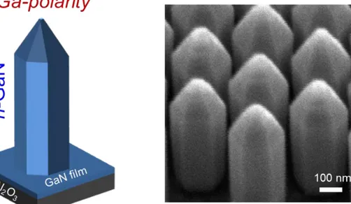
Text S5. Ga-polar n-GaN nanocrystal structure.
A polarity generally refers to the direction in which GaN grows considering Ga-N bonds that are collinear with the c-axis of the wurtzite crystal structure. The vector from Ga to
N-direction defines [0001], which is the positive N-direction of the c-axis (75). When the growth direction is [0001], i.e., Ga-polarity, the formation of pyramidal geometry is often observed for GaN nanowires. Conversely, the structure has N polarity when the growth direction is [0001̅], which often exhibits a flat top surface (76, 77). In the case of GaN wurtzite crystal structure, it is already well known that the polarity depends critically on the growth kinetics, buffer layers, substrates, and growth systems (78, 79). In this study, we first performed the epitaxial growth for only n-GaN segment. As shown in fig. S4, the n-GaN nanocrystals were formed as a pyramid shape with the Ga-polarity because of the Ga-terminated GaN template on Al2O3 substrate (76). Consequently, this Ga-polar crystal geometry leads to the formation
of a cone-shaped semi-polar multi-quantum disk layers in the active area.
Fig. S4. Ga-polar n-GaN nanocrystal structure. (A) Schematic illustration of the Ga-polar
n-GaN nanocrystal structure grown on GaN template. (B) FE-SEM image of the n-GaN nanocrystals which possess the Ga-polarity with a pyramid shape.
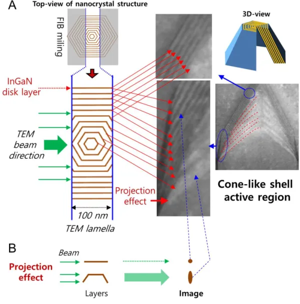
Text S6. Projection effect image and quasi-3D structure of InGaN/AlGaN quantum disk layers.
The 3D cone-like structure is expected from n-GaN nanocrystal structure as shown in fig. S4. Intriguingly, due to the quasi-3D structure of InGaN/AlGaN multi-quantum disk layers, the TEM images have different projection effects from the different layers, shown in fig. S5A. Figure S5B shows different TEM images from different projection effects by the overlapped layers and single layers.
Fig. S5. Projection effect in quasi-3D structure. (A) Schematic illustration of the FIB
milling region and TEM lamella structure and projection effects of quasi-3D structure of InGaN/AlGaN quantum disk layers in the active region. (B) Different projection effects in the InGaN/AlGaN quantum disk layers.
Text S7. Properties of semipolar InGaN/AlGaN core-shell heterostructures.
Optical properties of the semi-polar InGaN/AlGaN core-shell heterostructure were studied using photoluminescence (PL) spectroscopy. Shown in fig. S6 is the PL spectra measured at room temperature using a 405 nm laser as the excitation source. It is seen that the PL
intensity of the semi-polar InGaN/AlGaN core-shell is enhanced by nearly a factor of eight, compared to InGaN/GaN heterostructure without the formation of AlGaN shell. To examine the effect of an AlGaN shell on the optical emission properties, this study was performed on calibration samples under conditions without significant photonic band edge resonant effect. The shell structure spontaneously formed on the sidewalls of the active region can lead to drastically reduced non-radiative surface recombination due to the effective lateral confinement offered by the large band-gap AlGaN shell (54). Moreover, unique quasi 3D structure exhibits massively enhanced surface emission and improved carrier injection efficiency, due to the much larger active area (56). It is also well known that such semi-polar structure can effectively suppress the quantum-confined Stark effect (QCSE) due to the reduced polarization fields (55-57).
Fig. S6. PL emission spectra of InGaN/AlGaN core-shell multiquantum disk
nanocrystals (green curve) and InGaN/GaN multiquantum disk nanocrystals without AlGaN shell (blue curve) measured at 300 K.
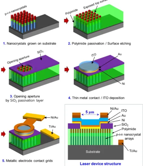
Text S8. NCSEL device fabrication.
The nanocrystal surface-emitting laser (NCSEL) device was fabricated by the following steps.
Fig. S7. Schematic illustration of the full device fabrication, including passivation, planarization, photolithography, and contact metallization techniques.
In order to achieve stable and low resistivity ohmic contact, we have performed extensive optimization of the thickness of Ni and Au and annealing process. Upon annealing, Ni may form NiOx and becomes nearly transparent (80, 81). The thin Au layer, however, does
partially block the emitted light. It is estimated that the transmittance of the Au metal layer is about 60-70% in the green wavelength region (81–83), which leads to non-negligible optical loss and limits the optical power. There is significant room to further optimize the fabrication process to improve the current injection and spreading and to enhance the device output
power. For example, nonuniform current injection, particularly at low current densities, may affect the photonic band edge resonance mode.
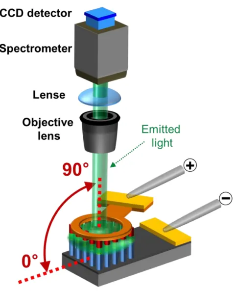
Text S9. Electroluminescence measurement.
The EL spectrum measurement involves the use of an objective lens and an iHR550
spectrometer with a CCD detector. The emitted light was collected from the top surface of the device, shown in fig. S8. The output power was measured using a Si photodiode sensor placed direclty on top of the device.
Text S10. Calculation of far-field radiation pattern.
The far-field radiation pattern of the nanocrystal laser structure is calculated by 3D-FDTD simulation using the commercial software package Lumerical FDTD Solutions 8.6. The nanocrystals are modelled to have flat top surface rather than pyramid top surface. The nanocrystals are arranged in a hexagonal region with a side length of ~3.5 μm. The
nanocrystal diameter and the lattice constant are the same as designed by 2D FEM simulation. The nanocrystals have three layers, including 370 nm n-GaN, 40 nm active region, and 190 nm p-GaN. The refractive index is 2.38 for n-GaN and p-GaN. The 40 nm active region has an effective refractive index of 2.56. A broadband TM polarized dipole source was used to fully excite all possible modes in the structure. Perfectly matched layer boundary condition was applied to minimize reflection at the simulation boundary. The simulation was performed for sufficiently long time to reach steady state. Only the data in the last 600 fs of the
simulation was used for calculation to avoid misinterpretation due to the transient stage. The near field of 50 nm above the nanocrystal array was used for calculating the far field radiation pattern.
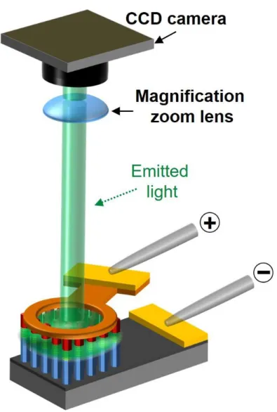
Text S11. Measurement of far-field radiation pattern.
For the far-field measurement, the light emission was collected by a high megapixel color charge coupled device (CCD) camera with a magnification zoom lens, which was placed at a distance from the top surface of the device. The arrangement was completely perpendicular to the NCSEL device surface, shown in fig. S9.
Fig. S9. Schematic illustration of the far-field measurement setup with a CCD camera at a distance above the NCSEL device.
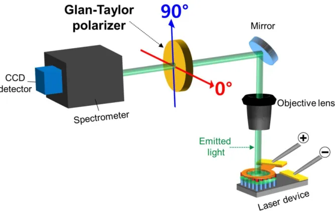
Text S12. Polarization measurement of the light emission of InGaN NCSELs.
The polarizer was installed on the top surface of the InGaN NCSEL, shown in fig. S10. The polarization was resolved by a Glan-Taylor calcite polarizer with a high-precision rotation mount system. The polarization angle was defined based on the nanocrystal structure as shown in fig. S10.