Publisher’s version / Version de l'éditeur:
Vous avez des questions? Nous pouvons vous aider. Pour communiquer directement avec un auteur, consultez
la première page de la revue dans laquelle son article a été publié afin de trouver ses coordonnées. Si vous n’arrivez pas à les repérer, communiquez avec nous à [email protected].
Questions? Contact the NRC Publications Archive team at
[email protected]. If you wish to email the authors directly, please see the first page of the publication for their contact information.
https://publications-cnrc.canada.ca/fra/droits
L’accès à ce site Web et l’utilisation de son contenu sont assujettis aux conditions présentées dans le site LISEZ CES CONDITIONS ATTENTIVEMENT AVANT D’UTILISER CE SITE WEB.
Smart Photonic and Optoelectronic Integrated Circuits XXII, Proceedings of
SPIE; no. 11284, pp. 112840K-1-112840K-6, 2020-03-05
READ THESE TERMS AND CONDITIONS CAREFULLY BEFORE USING THIS WEBSITE.
https://nrc-publications.canada.ca/eng/copyright
NRC Publications Archive Record / Notice des Archives des publications du CNRC :
https://nrc-publications.canada.ca/eng/view/object/?id=b8a6ebef-7490-4ad3-b784-6213a893d7e6
https://publications-cnrc.canada.ca/fra/voir/objet/?id=b8a6ebef-7490-4ad3-b784-6213a893d7e6
NRC Publications Archive
Archives des publications du CNRC
This publication could be one of several versions: author’s original, accepted manuscript or the publisher’s version. / La version de cette publication peut être l’une des suivantes : la version prépublication de l’auteur, la version acceptée du manuscrit ou la version de l’éditeur.
For the publisher’s version, please access the DOI link below./ Pour consulter la version de l’éditeur, utilisez le lien DOI ci-dessous.
https://doi.org/10.1117/12.2545061
Access and use of this website and the material on it are subject to the Terms and Conditions set forth at
Subwavelength grating metamaterial structures for integrated
photonics
Molina-Fernández, Iñigo; Wangüemert-Perez, Gonzalo; Ortega-Moñux,
Alejandro; Halir, Robert; De Oliva Rubio, Jose; Sánchez Postigo, Alejandro;
Luque-González, José Manuel; Hadif-Elhouati, Abdelfettah; Pereira-Martín,
Daniel; González-Andrade, David; Villafranca-Velasco, Aitor;
PROCEEDINGS OF SPIE
SPIEDigitalLibrary.org/conference-proceedings-of-spie
Subwavelength grating metamaterial
structures for integrated photonics
Molina-Fernández, I., Wangüemert-Perez, J. G.,
Ortega-Moñux, A., Halir, Robert, de Oliva Rubio, J., et al.
I. Molina-Fernández, J. G. Wangüemert-Perez, A. Ortega-Moñux, Robert
Halir, J. de Oliva Rubio, A. Sánchez-Postigo, J. M. Luque-González,
Abdelfettah Hadij-Elhouati, D. Pereira-Martín, D. González-Andrade, A. V.
Velasco, A. Herrero-Bermello, Jens H. Schmid, Pavel Cheben, J. Čtyroký,
"Subwavelength grating metamaterial structures for integrated photonics,"
Proc. SPIE 11284, Smart Photonic and Optoelectronic Integrated Circuits
XXII, 112840K (26 February 2020); doi: 10.1117/12.2545061
Subwavelength grating metamaterial structures for integrated
photonics
I. Molina-Fernández
a, J. G. Wangüemert-Pérez
a, A. Ortega-Moñux
a, Robert Halir
a, J. de Oliva
Rubio
a, A. Sánchez-Postigo
a,
J. M. Luque-González
a, Abdelfettah Hadij-Elhouati
a, D.
Pereira-Martín
a, D. González-Andrade
b, A. V. Velasco
b, A. Herrero-Bermello
b, Jens H. Schmid
c, Pavel
Cheben
c,
J. Čtyroký
da
Universidad de Málaga, Dept. de Ingeniería de Comunicaciones, 29010 Málaga, Spain;
bInstitute of
Optics, Spanish National Research Council, 28006 Madrid, Spain;
cNational Research Council
Canada, Ottawa, Ontario K1A 0R6, Canada;
dInstitute of Photonics and Electronics, CAS,
Chaberská 57, 182 51 Prague, Czech Republic
Tel: (+34) 952131311, e-mail: [email protected]
ABSTRACT
Integrated photonics devices, based in subwavelength grating (SWG) metamaterials, have shown unprecedented performance in a wide variety of situations. Since their proposal and first experimental demonstration in 2010 designers have made use of the new degrees of freedom provided by these structures to design advanced devices with improved capabilities. The extended design space provided by SWG structures has been successfully used to engineer the refractive index, the dispersion and, more recently, the waveguide birefringence, thus allowing novel advanced device design. In this invited talk we will review some of the advances made by our group in the field
Keywords: subwavelength gratings, anisotropy, homogenization, polarization management
1. INTRODUCTION
Integrated photonics devices, based in subwavelength grating (SWG) metamaterials, have shown unprecedented performance in a wide variety of situations. Since their proposal and first experimental demonstration in the 2010 seminal work from Canada NRC researchers [1] , designers have made use of the new degrees of freedom provided by these structures to design advanced devices in the silicon platform with unprecedented performance. The extended design space provided by SWG structures was first successfully used to engineer the refractive index of the equivalent material [2], then used to engineer the dispersion of waveguide modes [3][4] and only recently we have realized the new possibilities that these materials offer to tailor the waveguide birefringence and get novel advanced devices [5].
SWGs are periodic structures whose pith is below half the wavelength of light and thus behave as diffraction-less waveguides. Light propagation through SWG waveguides can be rigorously analyzed by means of Bloch-Floquet theory which shows that lossless propagation can be achieved in a similar way to electron propagation in periodic crystal [4]. When the pitch, Λ, of the structure is smaller than half of the wavelength of light λ, diffracting effects are frustrated, and
the structure behaves like a homogenous anisotropic medium. Indeed, in the deep subwavelength regime (Λ ≪λ), the
equivalent refractive indexes of the subwavelength material are given by nxx2= a/Λ n12+(1- a/Λ)2 n22and nzz-2= a/Λ n1 -2+(1- a/Λ)2 n
2-2for polarization parallel and perpendicular to the segment interfaces respectively, here n1 and n2 and the
refractive indexes of silicon and the cladding material [6]. While these approximate formulas are no longer valid for easily fabricable structures which usually have pitch closer to half of wavelength in the medium, the equivalence with a homogenous anisotropic medium is maintained up to the vicinity of the Bragg regime [7]. This equivalence can be conveniently used to carry out an efficient design process. Several design constraints must also be taken into account when dealing with SWG structures as: avoiding an excessive mode delocalization to suppress leakage to the silicon substrate [8] and controlling the jitter to reasonable levels for a certain device length [9].
Keynote Paper
Smart Photonic and Optoelectronic Integrated Circuits XXII, edited by Sailing He, Laurent Vivien, Proc. of SPIE Vol. 11284, 112840K · © 2020 SPIE · CCC code: 0277-786X/20/$21 · doi: 10.1117/12.2545061
Proc. of SPIE Vol. 11284 112840K-1
In this this keynote contribution we will review some of the latest work developed in our group concerning SWG modeling and device design. We have recently shown that SWG birefringence can be controlled by tilting the SWG segments [5] and based in this a new polarization beam splitter has been developed [10]. Also, SWG engineering allows the implementation of gradual index metamaterials. Building on this idea, and by means of an accurate modeling of SWG behavior, we have used GRIN lens fundamentals to design a spot size (x30) converter with sub-decibel insertion losses and reduced footprint [11]. We will also present recent results that have allowed us to design new advanced SWG based devices: broadband zeroth diffraction order surface fiber-to-chip coupler [12], wideband mode multiplexer [13], an extreme spot size converter (x75) based on a distributed Bragg deflector [14], and ultra-narrow band Bragg filters [15], [16].
2.
ANISOTROPY MANAGEMENT
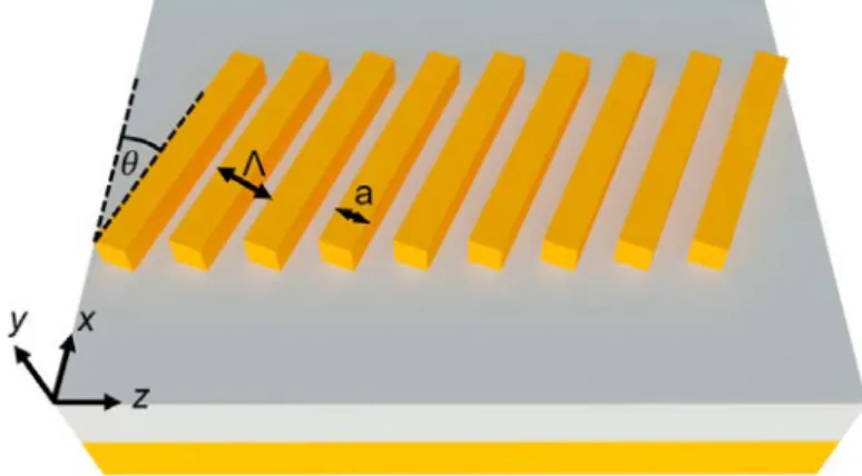
Fig. 1 illustrates a subwavelength waveguide where the individual segments have been tilted by an angle θ with respect
to the direction of propagation of light (z-axis). Let us initially consider θ = 0, so that the segments are oriented along the x-axis. In the deep subwavelength regime, i.e. when the pitch Λ of the structure is much smaller than the wavelength of
the light beam λ, the equivalent refractive indexes of the subwavelength material are given by nxx
2= a/Λ n 1
2
+(1- a/Λ)2 n2 2
and nzz-2= a/Λ n1-2+(1- a/Λ)2 n2-2for polarization parallel and perpendicular to the segment interfaces respectively, where
n1 and n2 and the refractive indexes of silicon and the cladding material [6]. The subwavelength structure thus behaves as
a homogeneous anisotropic metamaterial, i.e. as a uniaxial crystal with a permittivity tensor given by diag([nxx2,
nyy 2
=nxx 2
, nzz
2]) [7]. By choosing the adequate duty-cycle (a/Λ) the designer can thus lithographically define a
homogenous metamaterial with the equivalent index that best suits each device. The only restriction is that the pitch be small enough to frustrate Bragg reflection.
Note that the anisotropy can, to a certain degree be controlled by changing the duty cycle. However, this control is limited by two factors. First, a change in duty-cycle similarly affects TE and TM modes, e.g. increasing it results in higher effective indices for both polarizations. Second, in practice the range of variation of the duty-cycle is limited by fabrication constraints – it is preferable to keep it close to 50% to keep feature sizes as large as possible for a given pitch.
Figure 1. A subwavelength waveguide consists of periodically arranged segments of silicon and the cladding material with a spacing smaller than the wavelength of the propagating light. In the figure, the segments are spaced with a pitch Λ, the
duty-cycle is given by a/Λ, and light propagates along the z-axis. Such a structure is inherently anisotropic, and this anisotropy
can be controlled the tilt angle θ.
However, tilting the subwavelength segments by an angle θ provides an intriguing control over anisotropy without
requiring changes in the duty-cycle [5]. Specifically, this rotation translates into a “rotation” of the permittivity tensor which changes the nxx and nzz components but has no effect on the nyy element. This implies that increasing the tilt angle
from 0 will directly affect TE polarized modes (decreasing their effective index), while the effect on TM polarized modes is negligible. This approach thus offers completely new opportunities to control effective waveguide birefringence and on-chip polarization management.
3.
IMPLEMENTATION OF GRADUAL INDEX METAMATERIALS
On-Chip Gradual Index (GRIN) materials allow multiple interesting applications such as light collimation [17],[18],[19], crossing [18], multimode bending [20],[21] or invisibility [22]. The implementation of GRIN materials in SOI platforms usually requires non-standard fabrication processes, hindering the industrial exploitation of those GRIN based applications. Here we propose a methodology to implement GRIN metamaterials with single step lithography by engineering the shape of the segments of an SWG structure. In this process we take into account the intrinsic anisotropy of SWGs, accurately modelling the periodic structure as a GRIN homogeneous anisotropic metamaterial.
3.1 GRIN metamaterial implementation
To synthesize a Gradual refractive index, nGRIN, we use an SWG structure with shape modulated segments [See Fig.
2(a)]. In this process we are assuming that at any position x0, the local equivalent refractive index, nGRIN(x0), is given by
the equivalent refractive index of an x invariant SWG waveguide with the same duty cycle and period [See Fig. 2(b): Inset]. Following this assumption, we calculate the look-up table which maps any refractive into its corresponding duty cycles as outlined in Ref. [11]. Once the look-up table has been calculated, we proceed as follows [See Fig. 2(b)]: the local equivalent refractive index, nGRIN(x0), at any position x0, is implemented by seeking the duty cycle DC which
implements that index [Fig. 2(b), blue arrow from ① to ②]. This duty cycle is then imposed at the point x0 [Fig. 2(b),
blue arrow from ② to ③]. Once the duty cycle has been chosen, we are implicitly implementing an anisotropic GRIN metamaterial [Fig. 2(b), orange arrow from ② to ④], which in some applications, as the one shown here, helps to shorten the device length [11].
Figure 2. a) Schematic of the subwavelength structure. The shape of the silicon blocks synthesizes the required index profile of the GRIN lens. b) To implement the equivalent refractive index at any position x0, (marked as ①) we refer to a look-up table (marked as ②) constructed by analyzing the structure shown in the inset, obtaining the shape a(x0) (marked as ③). This in turn imposes the value of nzz(x0) (marked as ④). Inset: Schematic of the periodic structureused to calculate both polarizations of the look-up table.
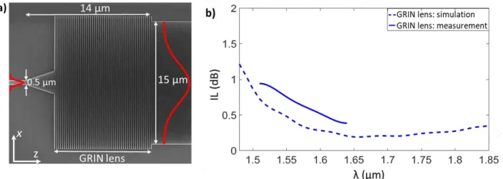
3.2 GRIN lens design
As a proof of concept of the GRIN metamaterial implementation, we design a GRIN lens which expands the field profile from a conventional 0.5 µm silicon wire to a 15 µm width waveguide [See Fig. 3(a)]. Our design achieves the proposed expansion in a length of 14 µm with measured Insertion Loss (IL) lower than 1 dB in a bandwidth of 130 nm, limited by our measurement setup, with 3D finite-difference time-domain (FDTD) simulations predicting a bandwidth in excess of 300 nm [See Fig. 3(b)].
To measure the tolerance of the device to fabrication error, we have also studied the IL of the nominal device when a ±10% duty cycle error is introduced. Our measurements predict that in all cases the IL are lower than 1 dB, showing and excellent tolerance to fabrication deviation.
Proc. of SPIE Vol. 11284 112840K-3
Figure 3. a) Scanning electron microscopy (SEM) image of the proposed spot size converter prior to the deposition of the SiO2 cladding. The device converts the guided mode of a conventional 500 nm wide silicon wire to the fundamental mode of a 15 µm wide waveguide. b) Insertion losses as a function of the wavelength for the nominal SWG lens design (blue lines). Measurements were performed using a back-to-back configuration, so measured insertion losses are divided by two. Our measurement setup is limited to the 1.51 µm < 𝜆𝜆 < 1.64 µm wavelength range
4.
SWG ANYSOTROPHY ENGINEERING FOR POLARIZATION SPLITTING
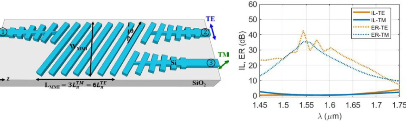
To cope with the strong dependence on the polarization of silicon photonic circuits, a wide variety of designs of polarization beam splitters (PBS) and rotators (PR) with high performance have been proposed as the main part of the polarization diversity circuits [23]. The properties of SWGs have also been exploited to overcome some of the limitations of conventional polarization beam splitters [24], [25], orientating, however, SWG segments only parallel and perpendicular to the direction of propagation, i.e. without leveraging a fine control over material anisotropy. Additionally, they often exhibit minimum feature sizes (MFS) below 100 nm and use specific cladding materials to achieve a good filling of the small gaps between the subwavelength elements, which results in a manufacturing limitation for many of the current opto-electronic foundries. By contrast, we design an MMI-based broadband polarization splitter exploiting, for the first time, the anisotropic properties of SWGs to circumvent these complex fabrication requirements. We tilt the SWG segments to enable a polarization independent control over the self-imaging lengths, therefore introducing the tilt angle as an additional degree of freedom [10].
The MMI-based PBS is shown in Fig. 4(a). For polarization splitting behavior, the beat lengths for TE and TM polarizations, LTE
π and LTMπ, must fulfill the polarization splitting condition (2mTM− 1) LTMπ= 2mTE LTEπ, where m is an
integer. The uniaxial crystal behavior of SWG results in a large difference between the beat lengths for TE and TM polarization and allows us to use mTE = mTM = 1, thereby minimizing device length. Moreover, titling the SWG segments
with respect to the transversal direction (x) provides direct control over the anisotropy of the equivalent medium, fine-tuning the beat length for both polarizations to fulfill the polarization splitting condition, LTM
π= 2LTEπ. Advantageously,
the duty cycle of the SWG structure can be kept constant at 50% to facilitate the manufacturing process, since it results in a maximization of the minimum feature size of the device, 110 nm; as well as to maintain a good confinement of the TM-polarization mode, avoiding leakage losses. The grating period was set at 220 nm in order to maximize the bandwidth for TE polarization, while ensuring that the structure operates in the SWG regime with negligible Bragg reflections.
The results, Fig. 4(b), demonstrate the broadband performance of the PBS with insertion losses (IL) below 1 dB and extinction ratios (ER) better than 20 dB for both polarizations in bandwidth in excess of 131 nm. At the central wavelength of 1.55 μm, the IL and ER are 0.32 dB and 36.4 dB for TE and 0.51 dB and 35.2 dB for TM polarization. Tolerance studies show that even in the presence of fabrication errors in the duty cycle and in the width of the MMI of the order of ± 11 nm and ± 20 nm, respectively, the bandwidth is remarkably constant and larger than 120 nm, resulting in full coverage of the C + L communication bands.
Fig. 4. (a) Polarization beam splitter based on an MMI composed of a tilted subwavelength grating. The width of the multimode region (WMMI) is 4 μm while its length (LMMI) is given by N𝛬𝛬cos(θ), where N is the number of SWG periods and 𝛬𝛬 is the structural period measured perpendicular to the segments. (b) Simulation results in terms of IL and ER.
ACKNOWLEDGEMENTS
The authors acknowledge funding from Alcyon Photonics (ref. nº 8.06/5.59.5045), Universidad de Málaga, Ministerio de Economía y Competitividad (MINECO) (TEC2016-80718-R), Ministerio de Educación, Cultura y Deporte (MECD) (FPU16/06762, FPU17/00638, FPU16/03401), and Fondo Europeo de Desarrollo Regional—FEDER
REFERENCES
[1] Przemek J. Bock, Pavel Cheben, Jens H. Schmid, Jean Lapointe, André Delâge, Siegfried Janz, Geof C. Aers, Dan-Xia Xu, Adam Densmore, and Trevor J. Hall, "Subwavelength grating periodic structures in silicon-on-insulator: a new type of microphotonic waveguide," Opt. Express 18, 20251-20262 (2010)
[2] Halir, R., Cheben, P., Schmid, J. H., Ma, R., Bedard, D., Janz, S., ... & Molina-Fernández, I. (2010), “Continuously apodized fiber-to-chip surface grating coupler with refractive index engineered subwavelength structure”, Optics letters, 35(19), 3243-3245
[3] A. Maese-Novo, Robert Halir, S. Romero-García, D. Pérez-Galacho, L. Zavargo-Peche, A. Ortega-Moñux, I. Molina-Fernández, J. G. Wangüemert-Pérez, and P. Cheben, "Wavelength independent multimode interference coupler," Opt. Express 21, 7033-7040 (2013)
[4] R. Halir, P. J. Bock, P. Cheben, A. Ortega-Moñux, C. Alonso-Ramos, J. H. Schmid, J. Lapointe, D.-X. Xu, J. G. Wangüemert-Pérez, Í. Molina-Fernández, et al.: Waveguide sub-wavelength structures: a review of principles and applications, Laser Photonics Rev., vol. 9, pp. 25–49, 2015
[5] José Manuel Luque-González, Alaine Herrero-Bermello, Alejandro Ortega-Moñux, Íñigo Molina-Fernández, Aitor V. Velasco, Pavel Cheben, Jens H. Schmid, Shurui Wang, and Robert Halir, "Tilted subwavelength gratings: controlling anisotropy in metamaterial nanophotonic waveguides," Opt. Lett. 43, 4691-4694 (2018) [6] Halir, R., Ortega-Moñux, A., Benedikovic, D., Mashanovich, G. Z., Wangüemert-Pérez, J. G., Schmid, J. H., ...
& Cheben, P. (2018), ”Subwavelength-grating metamaterial structures for silicon photonic devices”, Proceedings of the IEEE, 106(12), 2144-2157.
[7] Pavel Cheben, Robert Halir, Jens H. Schmid, Harry A. Atwater, David R. Smith, “Subwavelength integrated photonics,” Nature 560, pp. 565–572, 2018”
Proc. of SPIE Vol. 11284 112840K-5
[8] Sarmiento-Merenguel, J. D., Ortega-Moñux, A., Fédéli, J. M., Wangüemert-Pérez, J. G., Alonso-Ramos, C., Durán-Valdeiglesias, E., ... & Halir, R. (2016), “Controlling leakage losses in subwavelength grating silicon metamaterial waveguides”, Optics letters, 41(15), 3443-3446.
[9] Ortega-Moñux, A., Čtyroký, J., Cheben, P., Schmid, J. H., Wang, S., Molina-Fernández, Í., & Halir, R. (2017), “Disorder effects in subwavelength grating metamaterial waveguides”, Optics express, 25(11), 12222-12236. [10] A. Herrero-Bermello, J. M. Luque-González, A. V. Velasco, A. Ortega-Moñux, P. Cheben and R. Halir,
"Design of a Broadband Polarization Splitter Based on Anisotropy-Engineered Tilted Subwavelength Gratings," IEEE Photonics Journal, vol. 11, no. 3, pp. 1-8, June 2019, Art no. 6601508. doi:
10.1109/JPHOT.2019.2912335
[11] Luque-González, J. M., Halir, R., Wangüemert-Pérez, J. G., de-Oliva-Rubio, J., Schmid, J. H., Cheben, P., ... & Ortega-Moñux, A., “An Ultracompact GRIN-Lens-Based Spot Size Converter using Subwavelength Grating Metamaterials”, Laser & Photonics Reviews 2019.
[12] A. Sánchez-Postigo et al., “Broadband fiber-chip zero-order surface grating coupler with 0.4 dB efficiency”, Optics Letters 41, 3013 (2016)
[13] D. González-Andrade et al., "Ultra-Broadband Mode Converter and Multiplexer Based on Sub-Wavelength Structures", IEEE Photonics Journal, vol. 10, no. 2, pp. 1-10, April 2018, Art no. 2201010. doi: 10.1109/JPHOT.2018.2819364
[14] Hadij-ElHouati, A., Cheben, P., Ortega-Moñux, A., Wangüemert-Pérez, J. G., Halir, R., Schmid, J. H., & Molina-Fernández, Í., “Distributed Bragg deflector coupler for on-chip shaping of optical beams”, Optics Express, 27(23), 33180-33193, 2019
[15] Čtyroký, J., Wangüemert-Pérez, J. G., Kwiecien, P., Richter, I., Litvik, J., Schmid, J. H., ... & Cheben, P. (2018). Design of narrowband Bragg spectral filters in subwavelength grating metamaterial waveguides. Optics express, 26(1), 179-194.
[16] P. Cheben et al., Bragg filter bandwidth engineering in subwavelength grating metamaterial waveguides," Opt. Lett. 44, 1043 (2019).
[17] Levy, M. Abashin, K. Ikeda, A. Krishnamoorthy, J. Cunningham, Y. Fainman, “Inhomogenous Dielectric Metamaterials with Space-Variant Polarizability,” Phys. Rev. Lett. 98, 243901, 2007
[18] Wu, Q., Turpin, J. & Werner, D., “Integrated photonic systems based on transformation optics enabled gradient index devices”. Light Sci Appl 1, e38 (2012)
[19] Lalanne, P., Chavel, P., “Metalenses at visible wavelengths: past, present, perspectives” Laser & Photonics Reviews 2017, 11, 1600295.
[20] Gabrielli, L., Liu, D., Johnson, S. et al. “On-chip transformation optics for multimode waveguide bends,” Nat Commun 3, 1217 (2012)
[21] Xu, H., Shi, Y., “Ultra-Sharp Multi-Mode Waveguide Bending Assisted with Metamaterial Based Mode Converters” Laser & Photonics Reviews 2018, 12, 1700240
[22] Li, J., and Pendry, J.B., “Hiding under the carpet: a new strategy for cloaking,” Physical review letters 101.20 (2008)
[23] D. Dai, L. Liu, S. Gao, D.-X. Xu, and S. He, “Polarization management for silicon photonic integrated circuits,” Laser Photon. Rev. 7(3), 303-308 (2013).
[24] L. Xu, Y. Wang, A. Kumar, D. Patel, E. El-Fiky, Z. Xing, R. Li, and D. V. Plant, “Polarization beam splitter based on MMI coupler with SWG Birefringence engineering on SOI,” IEEE Photon. Technol. Let. 30(4), 403-406 (2018).
[25] H. Xu, D. Dai, and Y. Shi, “Ultra-broadband and ultra-compact on-chip silicon polarization beam splitter by using hetero-anisotropic metamaterials,” Laser Photon. Rev. 13(4), 1800349 (2019).