HAL Id: hal-00835886
https://hal.archives-ouvertes.fr/hal-00835886
Submitted on 26 Jun 2018HAL is a multi-disciplinary open access
archive for the deposit and dissemination of sci-entific research documents, whether they are pub-lished or not. The documents may come from teaching and research institutions in France or abroad, or from public or private research centers.
L’archive ouverte pluridisciplinaire HAL, est destinée au dépôt et à la diffusion de documents scientifiques de niveau recherche, publiés ou non, émanant des établissements d’enseignement et de recherche français ou étrangers, des laboratoires publics ou privés.
Undoped and Nd3+ doped Si-based single layers and
superlattices for photonic applications
Larysa Khomenkova, Christophe Labbé, Xavier Portier, Marzia Carrada,
Fabrice Gourbilleau
To cite this version:
Larysa Khomenkova, Christophe Labbé, Xavier Portier, Marzia Carrada, Fabrice Gourbilleau. Un-doped and Nd3+ Un-doped Si-based single layers and superlattices for photonic applications. physica status solidi (a), Wiley, 2013, 210 (8), pp.1532-1543. �10.1002/pssa.201200942�. �hal-00835886�
Undoped and Nd
3þ
doped Si-based
single layers and superlattices for
photonic applications
Larysa Khomenkova*,1y, Christophe Labbé1, Xavier Portier1, Marzia Carrada2, and Fabrice Gourbilleau1
1CIMAP (CEA/CNRS/Ensicaen/UCBN), 6 Boulevard Marechal Juin, 14050 Caen, France 2CEMES/CNRS, Université de Toulouse, 29 rue J. Marvig, 31055 Toulouse, France
Keywords: photoluminescence, rare-earth ions, RF magnetron sputtering, silicon nanostructures
*Corresponding author: e-mail:larysa.khomenkova@ensicaen.fr, Phone: þ33 231452671, Fax: þ33 231452655 †Permanent address: V. Lashkaryov Institute of Semiconductor Physics, 45 Pr. Nauky, 03028 Kyiv, Ukraine;
e-mailkhomenkova@rambler.ru
This work presents the benefits of the superlattice approach to control light emission properties of materials with Si nano-clusters and rare-earth ions. The undoped and Nd3þ-doped both
Si-rich-SiO2single layers and Si-rich-SiO2/SiO2superlattices
were grown by radio frequency magnetron sputtering. Their properties were investigated by means of spectroscopic ellipsometry, Fourier infrared transmission spectroscopy, transmission electron microscopy, and photoluminescence (PL) methods versus deposition conditions, annealing treatment, and superlattice design (doping and thickness of alternated sublayers). An intense Nd3þemission from as-deposited single
layers and superlattices was observed. The lower annealing temperature (below 900 8C) of the single layers and super-lattices favors the formation of amorphous Si clusters that act as effective sensitizers of rare-earth ions. The highest Nd3þ PL
intensity was achieved after a conventional annealing at about 600–800 8C in nitrogen flow for all samples. Crystallized Si-nanoclusters were formed in Si-rich-SiO2 single layers upon
annealing at 1000–1100 8C, whereas their formation in the superlattices occurred at higher temperatures (1100–1150 8C). The mechanism of Nd ions’ excitation via energy transfer from Si-nanoclusters and/or matrix defects, if any, is discussed.
1 Introduction Nowadays, continuous increase of the demand for energy saving stimulates not only the elaboration of novel materials and devices on their basis, but also gives new impact for development of effective approaches allowing significant improvement of the electrical and optical parameters of already known materials. The main bottleneck of Si-core CMOS technology was the indirect infrared bandgap of bulk crystalline silicon, hampered it to act as light emitter and to develop fully Si-based photonic devices. Much effort was straightforward for the investigation of different approaches able to overcome this Si drawback. Firstly, “infrared” Si bandgap was modified in porous silicon materials [1, 2] by means of chemical or electrochemical etching of bulk Si wafer in HF-based solution. As a result, an efficient “red” emission from such samples was achieved [1, 2]. Due to quantum confinement effect, the absorption edge of Si nanocrystals or nanoclusters (Si-ncs) was shifted to the visible spectral range that opened not only a possibility
to create light-emitting devices, but also to improve the performance of Si-based solar cells [3].
Among different based nanostructured materials, Si-ncs embedded in SiO2 host attract much attention. Their optical properties are tuned by the mean size of the Si-ncs [4, 5], whereas microelectronic applications of these materials demand the control of the Si-ncs density [6, 7].
Besides chemical and/or electrochemical etching of bulk Si wafers, other fabrication approaches such as ion implantation [8], electron beam evaporation [9], reactive evaporation [5, 10, 11], chemical vapor deposition [7, 12], sputtering [6, 13–16], etc. were used to produce Si-based nanostructures. Usually, the formation of Si-ncs is a two-step process. At first, the Si-rich-SiO2 (SRSO) single layer is fabricated and then, high temperature annealing is used for Si-ncs formation via a phase separation process [8–16].
In spite of many promising results obtained for different SRSO materials [4–16], the Si-ncs density and their sizes
cannot be tuned independently using single layer approach. Meanwhile, a fine control of the Si-ncs distribution is required to monitor the electronic and optical properties of future Si-ncs-based devices. In this regard, a superlattice approach (when SRSO layers are alternated with insulating barrier sublayers) appears as an effective tool. In this case, a physical confinement of the Si-ncs sizes is obtained by varying the SRSO layer thickness, whereas excess Si content controls the Si-ncs number. As a consequence, more functionalities of Si-ncs-based materials can be considered. In most cases, the role of alternating sublayers is played by the SiO2 ones [4–14, 17, 18]. They suppress the out-diffusion of Si atoms from SRSO layers during a phase separation process, favoring the lateral diffusion for Si-ncs formation and, as a consequence, a narrower Si-ncs size distribution is achieved. In spite of this achievement, it is still surprising that an application of superlattice structures to obtain an emission from rare-earth ions is not well addressed. It is known that absorption cross-section of rare-earth ions is about 10"18–10"20cm"2 for 4f–4f transitions and about 10"12cm"2, for 4f–5d ones [19]. However, these latter are observed in UV and vacuum UV regions, restricting their use for many applications. Thus, more effective excitation of 4f–4f transitions requires a host enabling excitation via energy transfer. In this regard, Si-ncs offer significant enhancement of the activity of rare-earth ions. Among them, the most addressed is Er3þ due to its promising application for optical communication [19, 20]. A lot of efforts were concentrated to obtain efficient emission from Er3þ-doped Si-rich-SiO2single layers [21, 22]. The Si-ncs incorporation allows increasing of absorption cross-section of Er3þ ions from 10"21cm"2 [19, 23] up to 10"16cm"2[24–27] due to effective energy transfer from Si-ncs towards Er3þ ions. For this purpose, visible broad-band excitation was used offering safe applications of these materials. In spite of these results, a superlattice approach was not well addressed. Only a few works reported an efficient Er3þ emission in the green and infrared spectral ranges [28, 29]. Unfortunately, the Si-based superlattices doped with other rare-earth ions (Tm3þ, Nd3þ, etc.) are not well considered [30, 31]. Meanwhile, the Nd3þ doped structures along with Er3þ-doped ones could find a wide application for medicine and communication technologies as it was shown for Nd3þdoped glasses [32] or single Nd3þ -doped SRSO films [31, 33, 34].
This paper reports on the properties of SRSO/SiO2 superlattices produced by RF magnetron sputtering. The effect of fabrication conditions and post-fabrication processing is analyzed in terms of formation of size- and density-controlled Si-ncs. The microstructure evolution, optical, and light emitting properties versus annealing conditions are discussed. Apart from un-doped SRSO/SiO2superlattices, their Nd3þ -doped counterparts are analyzed. An efficient emission from Nd-SRSO/SiO2superlattices submitted to lower-temperature annealing treatment is demonstrated. The analysis of Nd3þ ions’ excitation mechanism (i.e., their interaction with Si-ncs and/or matrix defects, if any) is discussed.
2 Experimental details The samples were fabricated by radio frequency magnetron sputtering. Prior to deposi-tion, the wafers were cleaned in a 10% HF water soludeposi-tion, rinsed in de-ionized water, and dried in N2flow. They were immediately placed in the “load-lock” chamber of deposition unit. Such cleaning procedure allows hydrogen-terminated Si surface to be obtained [35]. This step is important because thermal SiO2can affect the growth kinetics of SRSO layers and the properties of future thin SRSO layers via presence of some stresses between the film and the substrate [20].
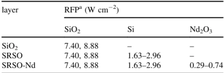
In this work, the samples (either single layers or superlattices) were deposited on 2-inches p-type Si substrates kept at 500 8C. The substrate rotation during deposition run allowed the fabrication of homogeneous samples. The total pressure of pure argon plasma was fixed at 3 mTorr. Other main deposition conditions are given in Table 1.
The SiO2layers were grown by sputtering of SiO2target. The SRSO ones were deposited by simultaneous co-sputtering of SiO2 and Si cathodes. The Si excess was monitored via RF power density applied on the Si cathode (RFP-Si) at other constant conditions. Doping of the samples with Nd3þions was performed during deposition process via simultaneous sputtering of Nd2O3target along with Si and SiO2ones.
The variation of Nd3þ content in the samples was monitored via a RFP-Nd2O3applied on this cathode. The Nd3þ content was estimated by means of Rutherford backscattering method. It was observed an increase of doping level from [Nd] ¼ 8 $ 1019at cm"3 (RFP-Nd2O3 ¼ 0.29 W cm"2) up to [Nd] ¼ 1021 at cm"3 (for RFP-Nd2O3¼ 0.59 W cm"2). The deposition time was tuned to grow the samples (as single layers as superlattices) with a thickness of about 120 nm.
For superlattices, SRSO layer thickness was kept at about 3 nm, whereas the SiO2one was in the range of 1.5– 5.0 nm. The number of stacks in the structures was monitored to keep a total thickness of about 120 nm. However, it is worth to point that the results will be mainly described for the samples made of 20 periods of 3-nm-SRSO/3-nm-SiO2stack, if any other parameters will not be mentioned.
An annealing treatment of single layers and superlattices was performed in a conventional furnace at 300–1150 8C
Table 1 Deposition conditions for undoped and Nd3þdoped
Si-based samples. layer RFPa(W cm"2) SiO2 Si Nd2O3 SiO2 7.40, 8.88 – – SRSO 7.40, 8.88 1.63–2.96 – SRSO-Nd 7.40, 8.88 1.63–2.96 0.29–0.74
aRFP is a power density applied for the corresponding cathodes (SiO 2, Si, or Nd2O3).
during 1–60 min in a nitrogen flow to investigate the formation of Si-ncs and to optimize the Nd3þ emitting parameters.
Spectroscopic ellipsometry was used to determine the thickness and refractive index of the as-deposited samples. The data were collected by means of a Jobin–Yvon ellipsometer (UVISEL) where the incident light was scanned in the 1.5–4.5 eV range under an incident angle of 66.38. The fitting of the experimental data was performed using DeltaPsi2 software [36]. Hereafter, the n values taken at 1.5 eV will be used for comparison. A Nicolet Nexus Fourier transform infrared (FTIR) spectrometer was used to investigate the infrared absorption spectra of the samples. FTIR spectra were measured under normal and Brewster (658) angle incidences.
Cross-sectional foils were prepared for TEM examina-tion by a standard mechanical procedure involving grinding, dimpling, and Arþ ion beam thinning until electron transparency. The samples were observed by conventional (CTEM) and high-resolution electron microscopy (HRTEM) using a FEG 2010 JEOL instrument operated at 200 keV. EFTEM was carried out on cross-sectional specimens using a field emission TEM, FEI Tecnai™ F20 microscope operated at 200 kV, equipped with a corrector for spherical aberration and a TRIDIEM Gatan Imaging Filter (GIF). This latter technique was used to observe the formation of Si clusters (crystallized and amorphous). EFTEM images were formed with electrons that are selected by a slit placed in the energy-dispersive plane of the spectrometer with a width of 4 eV centered at 17 eV (Si-plasmon energy).
Photoluminescence (PL) properties of the samples were investigated at room temperature. A 488 nm line from an Innova 90C coherent Arþ laser was used as the excitation source. This wavelength corresponds to a non-resonant excitation for Nd3þ ions. The PL spectra were recorded in the 500–1150 nm spectral range using a fast Hamamatsu R5108 photomultiplier tube (PMT) after dispersion of the light through a Jobin–Yvon TRIAX 180 monochromator linked with a SRS lock-in amplifier (SP830 DPS) referenced to the chopping frequency of light fixed at 20 Hz. Besides, a liquid-nitrogen cooled Ge-detector was used to detect the emission from Nd3þ-doped samples corresponding to the intra-4f shell transitions of Nd3þions, i.e., from the4F3/2level to the4I9/2 (0.92 mm), 4I11/2 (1.06 mm), and 4I13/2 (1.35 mm) levels. However, it did not allow correct simultaneous detection of visible PL emission from the samples. Thus, in the following, we present the spectra detected with a Hamamatsu R5108 PMT since 0.92 mm Nd3þluminescence transition and the Si-ncs emission can be detected simultaneously. This allowed simultaneous control of the PL properties of Si-ncs and different host defects (if any) and their interaction with Nd3þ ions. Since 0.92 mm Nd3þPL cannot be excited via bulk Si bandgap due to its smaller energy, it is obvious that Si-ncs and/ or host defects can be considered as sensitizers of Nd3þions. Thus, hereafter the PL spectra in the 500–1000 nm spectral range are presented for all the samples including Nd3þ-doped ones.
3 Results and discussion Let us briefly describe the properties of single undoped and Nd3þ-doped SRSO layers versus deposition conditions and annealing treatment to demonstrate the best choice for the deposition conditions for Si-based superlattices’ fabrication.
3.1 Effect of deposition conditions on the properties of single layers Numerous samples were fabricated with different deposition conditions to calibrate the deposition rate, layer stoichiometry and Nd3þ content (for the case of doped layers) to achieve Si-ncs formation as well as efficient Nd3þemission.
The samples stoichiometry was studied by means of spectroscopic ellipsometry (SE) and FTIR methods. The first approach is based on the correlation between the refractive index and Si-enrichment of SRSO layer [37], considering this latter as a heterogeneous mixture of amorphous Si and SiO2phases. Variation of Si content was monitored via the RF power applied on the Si target in the range RFP-Si ¼ 1.63–2.96 W cm"2. Note that monitoring of deposi-tion time was used to achieve constant thicknesses of the samples. This statement was confirmed by SE data demonstrating the efficient calibration of the deposition conditions. The spectroscopic variation of the refractive index, n, was also obtained and the results are presented in Fig. 1a for n taken at 1.5 eV light as a function of RFP-Si. To estimate the parameter of layers’ stoichiometry, xSE¼ [O]/[Si], from SE data we used the equation:
n ¼ 4 " 2:53x þ 0:63x2
ð1Þ proposed by Dehan et al. [37] for the n-value determined at 1.5 eV light energy. It was found the xSE value decreases
Figure 1 The refractive index, n (taken at 1.5 eV) (a) and the parameter of layer stoichiometry, x ¼ [O]/[Si], of SRSO layers (b) versus RFP-Si.
from 1.72 down to 1.48 when the RFP-Si increases from 1.63 W cm"2up to 2.96 W cm"2 (Fig. 1b).
It is worth to note, that doping of SRSO layers with Nd3þ ions does not affect the refractive index, when RFP-Nd2O3is below 0.44 W cm"2. However, n increases by Dn ' 0.02 when RFP-Nd2O3( 0.59 W cm"2. To explain this beha-vior, one can suppose that co-sputtering of Nd2O3target adds in the plasma not only rare-earth ions, but also oxygen ones. It is possible that more Si–O bonds are formed due to a chemical activity of oxygen, as well as Nd–Si–O bonds. These latter can favor the appearance of a material with higher refractive index. Taking into account the samples composition and the fact that SiO2 phase has a lower refractive index (n ¼ 1.45 at 1.5 eV), this increase of refractive index with RFP-Nd2O3 can be caused by the formation of small Nd–Si–O and/or Si agglomerates.
Analysis of FTIR spectra was also used to estimate the stoichiometric parameter (xFTIR). In this case, the peak position of Si–O TO3phonon measured for SRSO layers is compared to that obtained for pure SiO2with equal thickness grown with the same conditions. Besides, the analysis of the shape of FTIR spectra allowed the effect of Nd3þ ion incorporation on the distortion of the SRSO host, if any, to be observed.
It is known that continuous random network of SiO2 consists of corner-coordinated SiO4tetrahedra and disorder of amorphous structures comes from the Si–O–Si bond angle changes. Usually, SiO2possesses several vibration modes in the mid-infrared range originating mainly from the motion of oxygen atoms.
Under specific conditions, different LO and TO phonons of Si–O bond can be detected in the 450–1350 cm"1spectral range: at 1076 cm"1 (TO3) and 1256 cm"1 (LO3), at 1160 cm"1(TO4) and 1200 cm"1(LO4), at 810 cm"1(TO2) and 820 cm"1 (LO2), as well as at 457 cm"1 (TO1) and 507 cm"1(LO1) [38–40]. Additional incorporation of Si into SiO2 host leads to the shift of LO3 and TO3 phonons to lower-wave-numbers, as well as an increasing contribution of LO4–TO4doublet in the FTIR spectra [40, 46]. Moreover, in the case of high doping level in SiO2and/or SRSO with
rare-earth ions, the broadening of TO3phonon towards lower wave-numbers is also expected due to the incorporation of heavy ion into Si–O bonding similarly to that observed in Ref. [35].
To estimate the xFTIRvalue, the layer thickness effect on the TO3 phonon peak position (nTO3) has to be also
considered. It is known that the decrease of SiO2 layer thickness down to nanometer scale is accompanied by a shift of the peak positions of all vibration bands to lower wave numbers as well as by a decrease in the intensity of TO4–LO4 phonons that are usually ascribed to disordering of SiO2 matrix [39]. In the case of LO3and TO3phonons, this shift is about Dn ) 25–30 cm"1 [41]. Moreover, the detection of LO3 phonon is usually considered as an evidence of the formation of perfect Si/SiO2interface [42]. Thus, compari-son between samples with similar thicknesses grown with different deposition conditions allows the effect of silicon and rare-earth ions incorporation on the microstructure of the layers to be revealed.
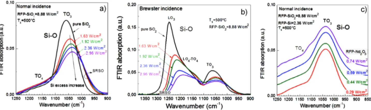
FTIR spectra of as-deposited SRSO layers, measured under normal incidence of the light excitation, are presented in Fig. 2a. The intense absorption band around 1000 cm"1 corresponds to the asymmetric stretching vibration of the oxygen atom in its twofold coordinated bridging bonding site (TO3phonon) [43]. As one can see, when the RFP-Si increases, the TO3phonon (ITO3) peak intensity decreases
accompanied by its broadening and by a shift of its position to lower wave-numbers.
This behavior is the evidence of higher Si incorporation into SiO2host resulting in a decrease of the number of Si–O bonds as well as in the broadening of TO3phonon (Fig. 2a). The FTIR spectra detected under Brewster incidence of the light excitation show a significant decrease of the LO3 phonon peak intensity, with a concomitant increase of the LO4–TO4doublet contribution (Fig. 2b). Since the layers investigated have close thicknesses, this behavior of FTIR spectra can be explained by higher Si incorporation into SiO2 host.
Based on the FTIR data, one can estimate the stoichiometric parameter (xFTIR ¼ [O]/[Si]). For this
Figure 2 FTIR spectra of as-deposited undoped (a and b) and Nd3þ-doped (c) SRSO single layers versus Si (a and b) and
RFP-Nd2O3(c) values measured at normal (a and c) and Brewster (b) incidence of light excitation. Deposition conditions are mentioned in the
purpose, a pure SiO2layer with the same thickness and a refractive index n ¼ 1.45 (at 1.5 eV) was grown with the same conditions from the SiO2target only. The TO3phonon of pure SiO2is peaked at nTO3 ¼ 1060 cm"1(Fig. 2a). This
value is lower than that of TO3phonon (1080 cm"1) usually referenced for thermal SiO2[38–43, 45]. This difference in the peak positions can be due to the lower thickness of our SiO2layer as well as its microstructure caused by the angle of Si–O–Si bonds [41]. This latter has a mean value of about 1448 with a full width at half maximum of about 358 (i.e., this angle can vary from 1258 up to 1808) for stoichiometric amorphous SiO2layers [44]. The variation of Si–O–Si angle affects the optical properties of SiO2layers leading to a shift of the TO3peak position.
Thus, to obtain correct xFTIRvalues, we performed this estimate based on the TO3peak position corresponding to our SiO2layers, using the equation:
xFTIR¼ 0:02vTO3" 19:2 ð2Þ
similarly to the approach described in Ref. [45]. Finally, a linear x decrease from 1.67 down to 1.49 was obtained for a RFP-Si variation from 1.63 W cm"2up to 2.96 W cm"2. Thus, these data confirm the monitoring of the Si content in SRSO layers via the RFP-Si parameter.
Comparison between xSEand xFTIRvalues obtained from SE and FTIR data shows that they are in good agreement (Table 2). However, higher x values (corresponding to lower Si content) obtained from FTIR data for higher RFP-Si values can be due to the FTIR insensitivity to the Si–Si vibration modes inside of some Si agglomerates.
Doping of SRSO layers with Nd3þ ions with RFP-Nd2O3* 0.44 W cm"2 at constant other conditions does not change the FTIR spectra significantly (Fig. 2c). However, for RFP-Nd2O3( 0.59 W cm"2, FTIR spectra show a TO3phonon peak broadening due to the formation of Si–O–Nd bonds. Note that Nd3þdoping does not affect the TO3peak position. The appearance of small feature at about 1110–1120 cm"1can be due to the formation of Si–O bonds in Si agglomerates (similarly to the Si–O presence in bulk crystalline Si materials).
3.2 Effect of annealing treatment of single layer properties Let us discuss the effect of thermal treatment on the evolution of SRSO layers and Si-ncs formation. It is known that annealing of SRSO layers at high temperature induces a phase separation between Si and SiO2 phases [5, 13, 16, 24, 34]. This process is reflected by a shift of TO3and LO3peak positions towards higher wave-numbers (Fig. 3a, c, and d), reaching the position of their counterparts corresponding to pure SiO2 (1075–1080 and 1255– 1260 cm"1, respectively) [37, 39]. Besides, the LO3 intensity increases, whereas the contribution of LO4–TO4 doublet decreases, revealing an improvement of matrix ordering [46] (Fig. 3).
Usually, the preferable increase of the LO3 peak intensity (ILO3) with respect to that of TO3phonon (ITO3)
is assigned to the nucleation and crystallization of the Si-ncs. Based on this assumption, one can see that in our case a phase separation begins at moderate temperatures (below 800 8C) evidenced by the shift of nTO3and nLO3from 1048 to
1065 cm"1 and from 1200 to 1225 cm"1, respectively (Fig. 3a and b). Along with this, the ILO3=ITO3 ratio is still
unchangeable, giving an assumption about the reconstruc-tion of Si–O and Si–Si bonds in Si–SiO4"x and Si–Six tetrahedra.
The gradual increase of the ILO3=ITO3 value for
TA ¼ 800–1000 8C is consistent with the formation of Si-nuclei that is more prominent for higher TAvalues. The shift of both phonon peaks to higher wave-numbers up to nTO3 ¼ 1078 cm"1and nLO3 ¼ 1250 cm"1is observed. For
TA ¼ 1050–1150 8C, the variations of nTO3 and nLO3 are
negligible, whereas ILO3=ITO3increases significantly. Such a
behavior is also indicative of the formation of Si-ncs and their crystallization at such annealing temperatures [41, 46]. Comparison between FTIR spectra of as-deposited undoped and Nd3þ-doped SRSO samples (grown with the same RFP-Si and RFP-Nd2O3 <0.44 W cm"2) revealed their similarity, which is also observed for all samples annealed at 1100 8C (Fig. 3c). These samples contain about [Nd] ' 1020at cm"3. Considering the FTIR method sensi-tivity, one can suppose the absence or negligible formation of Nd–Si–O bonds (i.e., Nd-clustering) in such layers (Fig. 3c). By contrast, the increase of RFP-Nd2O3 up to 0.74 W cm"2leads to the broadening of TO3phonon and an increase of the LO4–TO4 contribution not only for as-deposited samples, but also for annealed ones (Fig. 3d and e). An additional vibration band (or shoulder) in the 900– 980 cm"1spectral range appears. This is an evidence of the formation of Nd–Si–O bonds and Nd3þclustering in SRSO host. The increase of the Nd3þcontent up to [Nd] ' 1021 at cm"3makes such clustering more probable (Fig. 3c–e). Thus, FTIR spectra demonstrate a significant effect of the deposition and post-deposition conditions on microstructure of the samples affecting their optical and luminescent properties.
3.3 PL properties of undoped single layers The as-deposited layers did not demonstrate intense PL emission.
Table 2 The parameter of stoichiometry, x ¼ [O]/[Si], obtained from spectroscopic ellipsometry (xSE) and FTIR (xFTIR) data for
SRSO samples grown with different RFP-Si values. RFP-Sia(W/cm2) SE FTIR n1.5 eV xSE nTO3 xFTIR 1.63 1.56 1.60 1043.5 1.67 1.92 1.61 1.51 1041.5 1.63 2.36 1.65 1.46 1035.5 1.51 2.96 1.69 1.41 1034.5 1.49
aRFP is a power density applied on the Si cathode; SE, spectroscopic ellipsometry.
Sometimes, a weak red emission with the PL peak at about 730 nm was observed (not shown here). In such a case, it can be ascribed to SiOxdefects or some Si agglomerates formed during deposition at high temperature (500 8C) similarly to the results of Refs. [20, 24, 47]. To form Si-ncs, an annealing at 1100–1150 8C for 60 min in nitrogen flow is usually applied [3, 5, 11]. This treatment results also in an appearance of bright emission in the visible spectral range caused by either radiative exciton recombination inside Si-ncs embedded in SiO2or via Si/SiO2interface states and/or SiO2host defects. Thus, we studied, at first, the effect of an annealing treatment on the Si-ncs formation to optimize the emitting properties of the materials for future superlattices. Then, the effect of Nd3þ doping on the optimized SRSO layers was investigated.
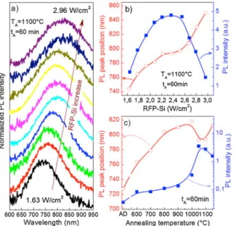
Figure 4a represents the PL spectra of the SRSO layers grown with different RFP-Si values and annealed at 1100 8C
during 60 min in nitrogen flow. As one can see, the increase of Si content in SRSO layers (monitored by the RFP-Si value) favors a shift of the PL peak position from about 745 nm (x ¼ 1.72, RFP-Si ¼ 1.63 W cm"2) to about 845 nm (x ¼ 1.49, RFP-Si ¼ 2.96 W cm"2) as well as a peak broadening (Fig. 4a and b). This behavior of PL peak position is explained by the formation of Si-ncs with larger mean size and wider distribution when Si content increases. The non-monotonous behavior of PL intensity can be caused by the increase of the number of Si-ncs when RFP-Si increases up to 2.2 W cm"2, whereas the PL quenching for RFP-Si >2.5 W cm"2 is due to formation of larger Si-ncs and contribution of non-radiative channel (e.g., Si dangling bonds). The highest PL intensity was observed for the SRSO single layers with x ¼ 1.5–1.6 (grown with RFP-Si ¼ 2.2– 2.5 W cm"2).
The effect of different annealing treatments on PL properties was investigated for SRSO samples fabricated with different conditions, but hereafter the most efficient samples will be described. Thus, the increase of the annealing temperature, TA, up to 1000 8C, enhances the PL intensity and favors the shift of its peak position from 730 nm (as-deposited sample) to 820 nm (TA¼ 1000 8C; Fig. 4c). The comparison of these results with the evolution of LO3and TO3phonons obtained from FTIR data for the same sample (Fig. 3b) allows to explain this PL behavior by the formation of amorphous Si nuclei (or agglomerates) and their growing with TA. The sharp increase of PL intensity
Figure 3 Evolution of FTIR spectra (a), peak positions of TO3
(nTO3) and LO3(nLO3) phonons as well as ILO3=ITO3ratio (b) versus
TAfor SRSO layer. (c) FTIR spectra of undoped (solid line) and
Nd3þ-doped SRSO (circle symbols) layers annealed at 1100 8C.
(d and e) FTIR spectra of as-deposited (d) and annealed at 1100 8C (e) Nd-doped SRSO layers grown RFP-Nd2O3¼ 0.29 W cm"2(1)
and 0.74 W cm"2 (2), demonstrating a formation of Si–O–Nd
complexes for higher Nd content. Spectra were normalized on the ILO3value. For (a–e) RFP-Si ¼ 2.36 W cm"2, tA¼ 60 min. FTIR
spectra presented in (a, c–e) were measured under Brewster incidence (658).
Figure 4 Effect of the RFP-Si on PL spectra (a), PL peak position and PL intensity (b) of SRSO single layers annealed at 1100 8C for 60 min. (c) Evolution of PL peak position and PL intensity with annealing temperature observed for the SRSO layer grown with RFP-Si ¼ 2.36 W cm"2 showing the highest PL intensity. The
data at “AD” corresponds to the PL parameters of as-deposited samples. Annealing time is 60 min.
observed for samples annealed at TA¼ 1050–1100 8C (Fig. 3b) and the “blue” shift of PL peak position due to the crystallization of Si agglomerates accompanied by Si/SiO2 interface shell formation. This latter provides the better confinement of the carriers inside Si-ncs leading to higher PL emission. Further TA rise up to 1150 8C results in a PL quenching and a slight shift of the PL peak position to 810 nm (Fig. 4c). This shift can be due to the expansion of the Si-ncs via a coalescence of the smaller Si-ncs, whereas the PL intensity decrease can be explained by a significant contribution of non-radiative channels (e.g., Si dangling bonds formed at the Si-ncs/SiO2host interface).
3.4 Properties of Nd3þ-doped single SRSO layers Investigation of light emission from Nd3þ-doped single SRSO layers was performed under excitation by 488 nm light wavelength. This is a non-resonant excitation of Nd3þ ions revealing an energy transfer from Si-ncs (or host-defects, if any) towards rare-earth ions. The intra-4f shell transitions of Nd3þ from the 4F3/2 level to the 4I9/2 (0.92 mm),4I11/2(1.06 mm), and4I13/2(1.35 mm) levels ions can be observed. Among them, 0.92 mm Nd3þPL transition cannot be excited via the bulk Si bandgap due to its lower energy. This particularity will be used to demonstrate an
interaction between Si-ncs and/or host defects with Nd3þ ions.
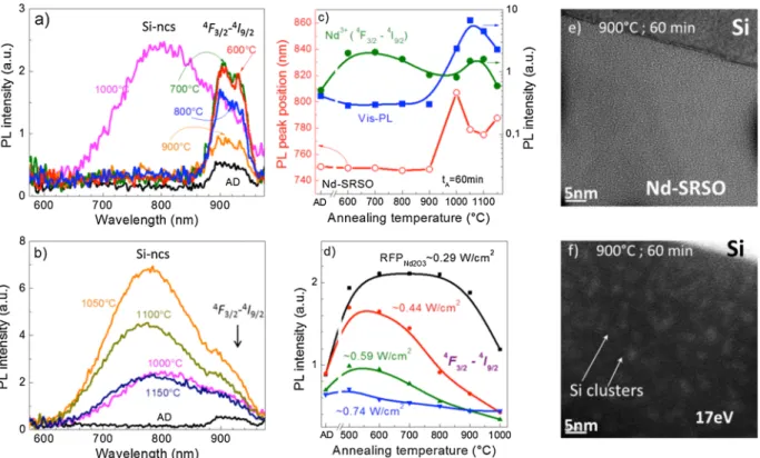
Figure 5a and b shows the PL emission of Nd3þ-doped SRSO samples versus TA. As one can see, as-deposited samples (AD) demonstrate Nd3þ PL band (at 0.92 mm) under non-resonant excitation (Fig. 5). This gives an evidence of the interaction between Nd3þ ions and Si agglomerates formed during deposition process, similarly to the phenomena described in our previous works for Er3þ-doped SRSO materials [47] and recently demonstrated for Nd3þ-doped SRSO layers with lower Si content [33, 34].
The annealing treatment results in the activation of Nd3þ emission. However, the dependence of its PL intensity versus TA has a non-monotonous behavior (Fig. 5c). The intense Nd3þemission is observed for the samples annealed at TA¼ 600–800 8C and 1050–1100 8C. In the first case, TA ¼ 600–800 8C, intense Nd3þ emission is due to an energy transfer from Si agglomerates. Their number decreases at TA¼ 900–1000 8C due to their coalescence that quenches Nd3þ PL emission. Further TA increase (1050–1100 8C) leads to the appearance of “visible” PL emission (due to Si-ncs formation) that, as a consequence, enhances Nd3þ luminescence (Fig. 5b and c). The PL intensity in the visible spectral range is similar to that
Figure 5 (a and b) Evolution of PL spectra of Nd-doped SRSO single layer versus TA. The spectra for as-deposited (AD) and annealed at
TA¼ 1000 8C samples are presented in both figures for comparison. (c) Variation of the peak position of visible PL component
(corresponding to Si-ncs emission) and its intensity as well as PL intensity of Nd3þ 4F
3/2–4I9/2 radiative transition with annealing
temperature. (d) Dependence of the Nd3þPL intensity (4F
3/2–4I9/2transition) for the layers grown with RFP-Nd2O3¼ 0.29–0.74 W cm"2
on annealing temperature. (e and f) Energy-filtered at 0 eV (e) and 17 eV (f) TEM images of the sample annealed at TA¼ 900 8C. For all
the figures the RFP-Si ¼ 2.36 W cm"2and t
described for undoped samples (Fig. 4c). This is an evidence of the sensitizing role of Si-ncs towards rare-earth ions (Fig. 5c).
At the same time, some difference between undoped and Nd3þ-doped SRSO layers can be seen from the comparison of the samples annealed at lower temperatures. Indeed, for TA¼ 600–900 8C, the peak position of the visible PL band is almost constant (about 750 nm; Fig. 5c), as opposed to that observed for undoped materials (gradual shift from 750 to 810 nm (Fig. 4c)). The weak visible emission is accompanied by an intense Nd3þPL with a slight decrease for TA¼ 900 8C (Fig. 5b). Since the formation of crystallized Si clusters is hardly believed upon such a treatment, one can assume an energy transfer from amorphous Si clusters towards Nd3þ ions. To confirm the presence of Si clusters (either amorphous or crystallized), these samples were investigated by TEM.
Thermal response of Nd3þ PL emission was also investigated for samples with different rare-earth contents. Figure 5d shows that high Nd3þ content leads to the quenching of Nd3þPL emission. However, the highest Nd3þ PL intensity for heavily doped samples can be achieved at lower TA. Thus, the most efficient Nd3þ PL emission for samples grown with RFP-Nd2O3¼ 0.29 W cm"2 ([Nd] * 1020at cm"3) was observed upon annealing treatment for TA¼ 600–800 8C, whereas for the layers grown with higher RFP-Nd2O3 ([Nd] ( 1021at cm"3), it was obtained with TA¼ 500–600 8C (Fig. 5d). This PL behavior of highly doped layers ([Nd] > 1021at cm"3) is explained by the higher probability of Nd3þ–Nd3þ interaction processes as well as significant host distortion leading to the contribution of non-radiative channels. Besides, the segregation of Nd3þ ions has to be also considered as it was demonstrated by the FTIR data (Fig. 3d and e). Similar rare-earth clustering and formation of the Nd2O3 phase was also observed for Nd3þ-doped SRSO materials with [Nd] ' 2.8 $ 1021at cm"3 (4.8 at%) and x ¼ 1.8, fabricated by reactive magnetron sputtering [31].
Taking into account these results, one can conclude that our Nd3þ-doped SRSO samples have an optimal Nd3þ content lower than 1021at cm"3. Thus, RFP-Nd2O3¼ 0.29 W cm"2 was used for the fabrication of Nd3þ-doped structures along with the other conditions described in Table 1. They allow the achievement of bright Nd3þ emission not only for samples annealed at high TA, but also for as-deposited layers and those submitted to thermal treatments at moderate temperatures (600–800 8C). In this case, the efficient excitation of Nd3þ ions is due to energy transfer from Si agglomerates. To confirm their presence (either amorphous or crystallized) for the samples annealed at moderate temperatures, the Nd-doped layers treated at TA¼ 900 8C for 60 min in nitrogen flow were investigated by TEM method.
Zero-loss energy-filtered TEM observation of Nd-doped sample annealed at TA¼ 900 8C for 60 min in nitrogen flow did not reveal any formation of crystallized grains (either Si-ncs or Nd-related ones; Fig. 5e). This means that the samples
remain amorphous upon annealing at TA* 900 8C. To reveal the presence of Si clusters, energy filtered TEM observations at 17 eV, corresponding to Si plasmon energy, were performed for the same sample. As shown in Fig. 5f, numerous amorphous Si-ncs were found in the samples. These results along with PL data confirm the sensitizing role of amorphous Si clusters towards rare-earth ions for the samples upon low-temperature annealing treatments (TA* 900 8C).
3.5 Properties of undoped and Nd-doped SRSO/ SiO2 superlattices Taking into account the results described above for single layers, we fabricated superlattices using the optimal deposition conditions (RFP-SiO2¼ 8.88 W cm"2 and RFP-Si ¼ 2.36 W cm"2
, as well as RFP-Nd2O3¼ 0.29 W cm"2(for Nd3þ doped sublayers)). The SRSO sublayer thickness was fixed at 3 nm (as for undoped and doped sublayers), whereas that of SiO2 sublayers was tuned in the 1.5–5.0 nm range. Considering the similar Si excess content in the SRSO sublayers, the annealing treatment at TA¼ 1100 8C can lead to the formation of Si-ncs with similar size distributions.
The investigation of PL properties of undoped super-lattices annealed at TA ¼ 1100 8C revealed a blue shift of PL peak position of the Si-ncs from about 745 nm (1.5 nm SiO2) via 733 nm (2.5 nm SiO2) down to 730 nm (3.8 nm SiO2; not shown here). This “blue” shift was accompanied by an increase of the PL intensity in one order of magnitude. It was explained by the fact that thinner SiO2 barriers cannot efficiently confine the Si atoms in SRSO layers and, thus, Si out-diffusion can occur. This favors Si-ncs formation with larger sizes (i.e., exceeding SRSO layer thickness). Thicker SiO2 barriers favor the physical confinement of Si atoms in SRSO sublayers as well as a better confinement of the carriers in the Si-ncs formed. This latter stimulates an enhancement of their PL intensity. It is worth to note that further increase of SiO2thickness (up to 5 nm) did not lead to a shift of PL peak position of Si-ncs. However, in terms of future application of SRSO/SiO2 superlattices, thicker SiO2 sublayers are undesirable due to higher resistivity of the whole structure [48]. Thus, hereafter, the properties of undoped and Nd-doped SRSO/ SiO2 superlaticces with 3 nm-SRSO and 3 nm SiO2 sublayers will be described.
Figure 6 shows the PL properties of superlattices versus annealing treatment. As one can see, an increase of the annealing temperature from 600 to 900 8C does not affect the PL peak position (760 nm), but it results in an increase of PL intensity. Further TArise stimulates an enhancement of PL emission up to some saturation (TA¼ 1100–1150 8C; Fig. 6a and b). Comparison between this PL behavior with that observed for single SRSO layer (Fig. 4c) shows that the formation of Si-ncs in the superlattices requires higher annealing temperatures. The highest PL intensity of single SRSO layer was achieved at 1050–1100 8C, while for SRSO/SiO2 superlattice, the most efficient emission is observed after annealing at 1100–1150 8C.
Similar results were observed in Ref. [17] and explained by the appearance of strain field at the SRSO/SiO2interfaces impeding a lateral diffusion of Si atoms in the SRSO sublayers. This allows supposing an amorphous nature of the Si-ncs in SRSO/SiO2 superlattices upon annealing at TA* 900 8C, whereas annealing at 1100–1150 8C favors Si-ncs crystallization. This thermal behavior of SRSO/SiO2 can also influence the Nd3þemission.
The analysis of PL spectra of undoped and Nd3þ-doped superlattices revealed similarities in the behavior of the peak positions of visible PL bands with TA (Fig. 6b and d). However, we observed about 30 nm “blue” shift of the PL peak position for doped samples annealed at TA¼ 500– 1100 8C (Fig. 6d). This “artificial” shift is due to the energy transfer from the larger Si clusters towards Nd3þ ions. Indeed, when this transfer is not efficient (TA¼ 1150 8C), both (undoped and doped) superlattices have the same PL peak position at about 770 nm (Fig. 6b and d). This is confirmed by the similar thicknesses and Si excess of SRSO sublayers in both (un)doped superlattices because the Si-ncs size distribution has to be similar.
The brightest Nd3þ emission is achieved for moderate annealing temperatures (TA¼ 600–800 8C; Fig. 6c and d). It is accompanied by the quenching of the visible emission from SRSO layers similarly to the case of Nd-doped SRSO single layers (Fig. 5). This correlation between PL intensity from Si-ncs and Nd3þ emission demonstrates the role of amorphous Si-ncs as effective sensitizers of rare-earth ions.
Further TAincrease results in a higher Si-ncs PL intensity and a simultaneous quenching of Nd3þemission (Fig. 6c and d). In spite of the increase of Si-ncs density, this quenching can be due to either the formation of Nd clusters or more likely the increase of the Nd-Si-ncs interaction distance. Since our single Nd-doped SRSO samples have [Nd] ' 1020at cm"3 and no evidence of the Nd clustering has been found, we can conclude that the Nd3þPL quenching is due to an increase of Si-ncs-Nd3þinteraction distance.
The benefits of the superlattice approach can be seen from the comparison of the Nd3þPL decay time obtained for Nd-doped SRSO single layer and Nd-SRSO/SiO2 super-lattice (Fig. 6e and f). This latter demonstrates higher Nd3þ life time (about 60 ms for TA¼ 700–900 8C) in comparison with that observed for single layer approach (about 15 ms). The shorter life-time in the last case can be due to the high Si excess content. Similar effect was observed for the Er3þ -doped SRSO layers grown with the same approach [47]. Both single layer and superlattices demonstrate an increase of the life-time with TA (Fig. 6e and f), whereas the total intensity of Nd3þPL emission decreases (Fig. 6b and d). The life-time increase is due to an improvement of the Nd3þ environment (via a recovering of Si–O bond angle towards that of SiO2 host (Fig. 3)), whereas the PL quenching is caused by the Si-ncs number decrease (due to their sizes’ increase) and by the increase of the Si-ncs-Nd3þinteraction distance. Besides, the Nd3þ clustering can also affect PL properties. However, in the case of superlattice structures,
Figure 6 PL properties evolution of undoped (a and b) and Nd-doped (c–e) SRSO/SiO2superlattices for different annealing temperatures;
tA¼ 60 min. Parts (e) and (f) represent the effect of annealing temperature on the Nd3þPL life-time for the4F3/2–4I9/2radiative transition
(0.92 mm) obtained for Nd3þ-doped SRSO single layer and Nd3þ-SRSO/SiO
this effect is much less pronounced that is evidenced by the higher Nd3þPL life-time (Fig. 6f).
We carried out TEM observations for the investigation of the Si-ncs formation in our superlattices. The bright and dark field images are presented in Fig. 7. As one can see, both annealed samples conserve the periodicity of the structures. However, the sample annealed at TA¼ 700 8C during 60 min is still amorphous; no formation of crystallized Si-ncs was revealed. Annealing at 1100 8C during 60 min showed the presence of numerous crystallized Si-ncs, confined in the SRSO sublayers.
Note that in this case, any Nd3þ-rich cluster with a size larger than 2 nm was not seen. Meanwhile, this cannot allow us to conclude definitely about either their presence or absence in the samples. It is known that rare-earth ions have an ability for clustering in SiO2-based hosts and this is more likely for low atomic numbers of lanthanide ions [49, 50]. We could then suppose the presence of such Nd3þ-rich small clusters in our samples containing about [Nd] ' 1020at cm"3similarly to the case described for Er3þ-doped SRSO single layers grown by the same sputtering approach and annealed at 1100 8C [51]. We observed that about 30% of the total Er3þamount form these clusters leading to the quenching of their emitting activity. A similar investigation
of Nd-doped SRSO samples with different Nd contents described above by the atom probe technique is in progress. The results described above demonstrate that Si-ncs (either amorphous or crystallized) are effective sensitizers of rare-earth ions. Earlier, we showed that some host defects such as Si-oxygen deficient centers (Si-ODC), can effec-tively transfer energy towards Er3þions [28, 52] under high energy excitation (X-ray or ultraviolet-blue excitation). Similar data were obtained for Nd3þ-doped SRSO layers demonstrating efficient short-wavelength excitation of Nd3þ ions. Although in all our study we used 488-nm excitation light, we cannot rule out the presence of some host defects in our samples able to contribute to the Nd3þ excitation process. To investigate the role of the defects of SiO2host on Nd3þPL emission, along with Nd-SRSO/SiO2superlattices, we fabricated structures, where either both sublayers or only SiO2barriers were Nd3þ-doped and studied the annealing treatment effect on PL properties of the structures.
3.6 Effect of sublayers’ doping on PL properties of superlattices As shown above, among the different key parameters governing the optical properties of superlattices, the thickness of each type of sublayers plays an important role. Along with this, the location of rare-earth ions (either in SRSO or SiO2only, or in both sublayers simultaneous) also has to be considered. Thus, besides the Nd-SRSO/SiO2 superlattices, the Nd-SRSO/Nd-SiO2 and SRSO/Nd-SiO2 samples were fabricated. Thermal treatments were per-formed at different temperatures (600–1150 8C). However, Fig. 8 shows PL spectra for two specific annealing regimes, 700 8C (the most intense emission from Nd3þ ions) and 1100 8C (the highest Si-ncs emission). An annealing at 1100 8C results in a visible emission. Its PL peak position is almost constant for all three sets of samples that is an evidence of similar Si-ncs distribution in the structures (Fig. 8). The highest visible PL intensity is observed for
Figure 7 Bright and dark field TEM images of Nd-SRSO/SiO2
superlattice annealed at TA¼ 700 8C (a) and 1100 8C (b) for
60 min in nitrogen flow. The inset in (a) is a selected area electron diffraction (SAED) image confirming the amorphous nature of the sample. The inset in (b) is a filtered Fourier transform (FFT) image from a bright spot (marked as a ring) showing the (111) Si planes and thus, the formation of crystallized Si-ncs.
Figure 8 PL spectra of SRSO/SiO2superlattices partly or fully
doped with Nd3þ ions. Annealing temperatures were 700 and
SRSO/Nd-SiO2 structures, whereas the lowest value is obtained for fully doped superlattices (Fig. 8).
Since TEM data confirmed the formation of Si-ncs in the SRSO layers (Fig. 7b), this PL behavior from different superlattices can be explained by the fact that for SRSO/Nd-SiO2samples, only Si-ncs close to SRSO/SiO2 interface can participate to the excitation of Nd3þions. This results in a slight quenching of own Si-ncs emission. In the case of Nd-SRSO/SiO2and Nd-SRSO/Nd-SiO2the Si-ncs act as sensitizers of Nd3þ ions located either in SRSO or both SRSO and SiO2sublayers, being, in the last case, very close to the SRSO/SiO2 interface. The analysis of the PL intensities shows comparable Si-ncs PL amplitudes for SRSO/Nd-SiO2and Nd-SRSO/SiO2structures whereas for the fully doped structure, PL of Si-ncs has twice less intensity. This is an additional argument for the Si-ncs interaction with the Nd3þ ions located in a vicinity of the SRSO/SiO2 interfaces. Another argument of the Si-ncs quenching could be a formation of some Nd-rich clusters that can act as non-radiative channels.
The most efficient Nd3þemission was achieved for Nd-SRSO/SiO2structures (Fig. 8). Its quenching with TAcan be due to a mismatching between the Nd3þlevels and the Si-ncs bandgap, governed by higher annealing temperature as it was shown in Ref. [53] for Nd-doped SRSO samples. Although, in most cases, the excitation mechanism of Nd3þ ions is considered to be similar to the Si-ncs-Er3þ interaction, the different nature of Nd3þions requires more investigation to reveal the ways of their efficient excitation.
The highest Nd3þ emission for Nd-SRSO/SiO2 super-lattices was obtained upon annealing at 700 8C. However, a comparable Nd3þintensity was also deteced for Nd-SRSO/ Nd-SiO2 (Fig. 8). Thus, based on the assumption that amorphous Si agglomerates (or nanoclusters), formed in the SRSO layers at TA¼ 700 8C, can act as efficient sensitizers of Nd3þ ions, we have to assume that the energy transfer occurs from Si-ncs towards Nd3þions not only for the ions located in the Nd-SRSO sublayers, but also in the vicinity of the Nd-SRSO/Nd-SiO2interfaces. However, this assump-tion cannot only be a reason for this intense PL emission, because an efficient Nd3þPL was found for SRSO/Nd-SiO2 structures, where only SiO2sublayers were doped with Nd3þ ions. Thus, in this case, we have to assume: (i) either a contribution of additional excitation channel for Nd3þions. This latter can be some host defects (for instance, Si-ODC) that can interact with Si-ncs and Nd3þions similar to the case described for Er3þ-doped SRSO materials [52]; (ii) or the possibility for Nd3þ ions to diffuse towards SRSO/SiO2 interfaces. Since SRSO and SiO2 materials have different lattice parameters and SRSO is usually stressed, the appearance of the strain field at the SRSO/SiO2interfaces in the superlattices can be a driving force for Nd3þdiffusion towards the interfaces. However, this issue needs further investigation.
It is worth to note that an effect of other alternated sublayers on the Nd3þemission is the matter of future work. Recently, a lot of studies have been focused on Si nitrides or
oxynitrides because of their potential use as alternating barrier materials [3, 54, 55]. They offer a better conductivity in comparison with SiO2barriers [48] as well as a promising optical activity of Nd3þions [56]. However, the mechanism of their excitation is still debatable and requires deeper investigations for effective control of rare-earth emission.
4 Conclusions This work presents the benefits of the superlattice approach to control microstructure and light emission properties of Si nanoclusters and rare-earth ions. The post-fabrication processing showed that the formation of Si-ncs in SRSO/SiO2 superlattices occurs at higher annealing temperatures than in single SRSO layers. The efficient Nd3þemission was achieved at moderate annealing temperatures (600–800 8C). It was demonstrated that amorphous Si nanoclusters are efficient sensitizers of rare-earth ions.
Acknowledgements This work was supported by the French National Research Agency (ANR) through Nanoscience and Nanotechnology Program (DAPHNES project ANR-08-NANO-005). Authors would like to thank Dr. J. Perrière from Institut des NanoSciences de Paris (INSP/CNRS, Paris) for RBS measurements.
References
[1] L. T. Canham, Appl. Phys. Lett. 57, 1046 (1990).
[2] V. Lehmann and U. Gösele, Appl. Phys. Lett. 58, 856 (1991). [3] G. Conibeer, M. Green, E.-Ch. Cho, D. König, Y.-H. Cho, T. Fangsuwannarak, G. Scardera, E. Pink, Y. Huang, T. Puzzer, S. Huang, D. Song, C. Flynn, S. Park, X. Hao, and D. Mansfield, Thin Solid Films 516, 6748 (2008).
[4] D. J. Lockwood, Z. H. Lu, and J. M. Baribeau, Phys. Rev. Lett. 76, 539 (1996).
[5] M. Zacharias, J. Heitmann, R. Scholz, U. Kahler, M. Schmidt, and J. Bläsing, Appl. Phys. Lett. 80, 661 (2002).
[6] C. L. Heng, B. R. Zhang, Y. P. Qiao, Z. C. Ma, W. H. Zong, and G. G. Qin, Physica B 270, 104 (1999).
[7] B. Berghoff, S. Suckow, R. Rölver, B. Spangenberg, H. Kurz, A. Sologubenko, and J. Mayer, J. Appl. Phys. 106, 083706 (2009).
[8] K. S. Min, K. V. Shcheglov, C. M. Yang, H. A. Atwater, M. L. Brongersma, and A. Polman, Appl. Phys. Lett. 69, 2033 (1996).
[9] D. Li, Y.-B. Chen, Y. Ren, J. Zhu, Y.-Y. Zhao, and M. Lu, Nanoscale Res. Lett. 7, 200 (2012).
[10] U. Kahler and H. Hofmeister, Opt. Mater. 17, 83 (2001). [11] J. Heitmann, R. Scholz, M. Schmidt, and M. Zacharias,
J. Non-Cryst. Solids 299–302, 1075 (2002).
[12] Z. X. Ma, X. B. Liao, J. He, W. C. Cheng, G. Z. Yue, Y. Q. Wang, and G. L. Kong, J. Appl. Phys. 83, 7934 (1998). [13] C. Ternon, F. Gourbilleau, X. Portier, P. Voivenel, and C.
Dufour, Thin Solid Films 419, 5 (2002). [14] S. Y. Ma, Thin Solid Films 402, 222 (2002).
[15] S. Hayashi and K. Yamamoto, J. Lumin. 70, 352 (1996). [16] L. Khomenkova, N. Korsunska, V. Yukhimchuk, B.
Jumayev, T. Torchynska, A. Vivas Hernandez, A. Many, Y. Goldstein, E. Savir, and J. Jedrzejewski, J. Lumin. 102, 705 (2003).
[17] T. Zheng and Z. Li, Superlattices Microstruct. 37, 227 (2005). [18] M. Roussel, E. Talbot, F. Gourbilleau, and P. Pareige,
Nanoscale Res. Lett. 6, 164 (2011).
[19] A. J. Kenyon, Semicond. Sci. Technol. 20, R65 (2005). [20] S. Cueff, C. Labbé, O. Jambois, B. Garrido, X. Portier, and R.
Rizk, Nanoscale Res. Lett. 6, 395 (2011).
[21] M. Wojdak, M. Klik, M. Forcales, O. B. Gusev, T. Gregorkiewicz, D. Pacifici, G. Franzò, F. Priolo, and F. Iacona, Phys. Rev. B 69, 233315 (2004).
[22] O. Jambois, F. Gourbilleau, A. J. Kenyon, J. Montserrat, R. Rizk, and B. Garrido, Opt. Express 18, 2230 (2010). [23] J. Miniscalco, J. Lightwave Technol. 9, 234 (1991). [24] S. Cueff, C. Labbé, J. Cardin, J.-L. Doualan, L. Khomenkova,
K. Hijazi, O. Jambois, B. Garrido, and R. Rizk, J. Appl. Phys. 108, 064302 (2010).
[25] A. Podhorodecki, J. Misiewicz, F. Gourbilleau, J. Cardin, and C. Dufour, Electrochem. Solid-State Lett. 13(3), K26 (2010). [26] J. M. Khoshman, A. Khan, and M. E. Kordesch, Surf. Coat.
Technol. 202, 2500 (2008).
[27] O. Stenzel, S. Wilbrandt, S. Yulin, N. Kaiser, M. Held, A. Tünnermann, J. Biskupek, and U. Kaiser, Opt. Mater. Express 1, 278 (2011).
[28] M. Schmidt, M. Zacharias, S. Richter, P. Fischer, P. Veit, J. Bläsing, and B. Breeger, Thin Solid Films 397, 211 (2001). [29] F. Gourbilleau, R. Madelon, C. Dufour, and R. Rizk, Opt.
Mater. 27, 868 (2005).
[30] K. Watanabe, H. Tamaoka, M. Fujii, K. Moriwaki, and Sh. Hayashi, Physica E 13, 1038 (2002).
[31] O. Debieu, D. Bréard, A. Podhorodecki, G. Zatryb, J. Misiewicz, C. Labbé, J. Cardin, and F. Gourbilleau, J. Appl. Phys. 108, 113114 (2010).
[32] J. H. Campbell and T. I. Suratwala, J. Non-Cryst. Solids 263– 264, 318 (2000).
[33] F. Gourbilleau, D. Bréard, C. Dufour, and R. Rizk, Opt. Mater. 31, 479 (2009).
[34] C.-H. Liang, O. Debieu, Y.-T. An, L. Khomenkova, J. Cardin, and F. Gourbilleau, J. Lumin. 132, 3118 (2012).
[35] L. Khomenkova, C. Dufour, P.-E. Coulon, C. Bonafos, and F. Gourbilleau, Nanotechnology 21, 095704 (2010).
[36] http://www.horiba.com.
[37] E. Dehan, P. Temple-Boyer, R. Henda, J. J. Pedroviejo, and E. Scheid, Thin Solid Films 266, 14 (1995).
[38] C. T. Kirk, Phys. Rev. B 38, 1255 (1988). [39] P. Lange, J. Appl. Phys. 66, 201 (1989).
[40] P. Innocenzi, J. Non-Cryst. Solids 316, 309 (2003). [41] H. Ono, T. Ikarashi, K. Ando, and T. Kitano, J. Appl. Phys.
84, 6064 (1998).
[42] J. E. Olsen and F. Shimura, J. Appl. Phys. 66, 1353 (1989). [43] D. V. Tsu, G. Lucovsky, and B. N. Davidson, Phys. Rev. B
40, 1795 (1989).
[44] M. G. Tucker, D. A. Keen, M. T. Dove, and K. Trachenko, J. Phys.: Condens. Matter 17, S67 (2005).
[45] P. G. Pai, S. S. Chao, Y. Takagi, and G. Lukovsky, J. Vac. Sci. Technol. A 4, 689 (1986).
[46] F. Gourbilleau, L. Khomenkova, D. Bréard, C. Dufour, and R. Rizk, Physica E 41, 1034 (2008).
[47] K. Hijazi, R. Rizk, J. Cardin, L. Khomenkova, and F. Gourbilleau, J. Appl. Phys. 106, 024311 (2009).
[48] R. Pratibha Nalini, P. Marie, J. Cardin, C. Dufour, P. Dimitrakis, P. Normand, M. Carrada, and F. Gourbilleau, Energy Proc. 10, 161 (2011).
[49] F. Rocca, C. Armellini, M. Ferrare, G. Dalba, N. Diab, A. Kuzmin, and F. Monti, J. Sol-Gel Sci. Technol. 26, 267 (2003).
[50] S. Sen and J. F. Stebbins, J. Non-Cryst. Solids 188, 54 (1995). [51] E. Talbot, R. Lardé, P. Pareige, L. Khomenkova, K. Hijazi,
and F. Gourbilleau, Nanoscale Res. Lett. 8, 39 (2013). [52] S. Cueff, C. Labbé, B. Dierre, F. Fabbri, T. Sekiguchi, X.
Portier, and R. Rizk, J. Appl. Phys. 108, 113504 (2010). [53] S.-Y. Seo, H.-S. Han, and J. H. Shin, J. Korean Phys. Soc. 39,
S78 (2001).
[54] S. Saito, T. Takahama, K. Tani, M. Takahashi, T. Mine, Y. Suwa, and D. Hisamoto, Appl. Phys. Lett. 98, 261104 (2011). [55] L. Ding, M. B. Yu, X. Tu, G. Q. Lo, S. Tripathy, and T. P.
Chen, Opt. Express 19, 2729 (2011).
[56] R. Pratibha Nalini, L. Khomenkova, O. Debieu, J. Cardin, C. Dufour, M. Carrada, and F. Gourbilleau, Nanoscale Res. Lett. 7, 124 (2012).
![Figure 1 The refractive index, n (taken at 1.5 eV) (a) and the parameter of layer stoichiometry, x ¼ [O]/[Si], of SRSO layers (b) versus RFP-Si.](https://thumb-eu.123doks.com/thumbv2/123doknet/12955606.376309/4.892.458.772.727.1058/figure-refractive-index-taken-parameter-stoichiometry-layers-versus.webp)
![Table 2 The parameter of stoichiometry, x ¼ [O]/[Si], obtained from spectroscopic ellipsometry (x SE ) and FTIR (x FTIR ) data for SRSO samples grown with different RFP-Si values.](https://thumb-eu.123doks.com/thumbv2/123doknet/12955606.376309/6.892.85.442.954.1085/table-parameter-stoichiometry-obtained-spectroscopic-ellipsometry-samples-different.webp)