HAL Id: hal-03102784
https://hal.archives-ouvertes.fr/hal-03102784
Submitted on 7 Jan 2021HAL is a multi-disciplinary open access archive for the deposit and dissemination of sci-entific research documents, whether they are pub-lished or not. The documents may come from teaching and research institutions in France or abroad, or from public or private research centers.
L’archive ouverte pluridisciplinaire HAL, est destinée au dépôt et à la diffusion de documents scientifiques de niveau recherche, publiés ou non, émanant des établissements d’enseignement et de recherche français ou étrangers, des laboratoires publics ou privés.
Ferroelectric Gating of Narrow Band-Gap Nanocrystal
Arrays with Enhanced Light Matter Coupling
Charlie Gréboval, Audrey Chu, Debora Magalhaes, Julien Ramade, Junling
Qu, Prachi Rastogi, Adrien Khalili, Sang-Soo Chee, Hervé Aubin, Grégory
Vincent, et al.
To cite this version:
Charlie Gréboval, Audrey Chu, Debora Magalhaes, Julien Ramade, Junling Qu, et al.. Ferroelec-tric Gating of Narrow Band-Gap Nanocrystal Arrays with Enhanced Light Matter Coupling. ACS photonics, American Chemical Society„ 2021, 8 (1), pp.259-268. �10.1021/acsphotonics.0c01464�. �hal-03102784�
Ferroelectric Gating of Narrow Band-Gap Nanocrystal Arrays with Enhanced Light Matter
Coupling
Charlie Gréboval
1, Audrey Chu
1, Debora Vale Magalhaes
2,3, Julien Ramade
2,3, Junling Qu
1, Prachi
Rastogi
1, Adrien Khalili
1, Sang-Soo Chee
1, Hervé Aubin
4, Grégory Vincent
5, Sara Bals
2,3,
Christophe Delerue
6, Emmanuel Lhuillier
1*1
Sorbonne Université, CNRS, Institut des NanoSciences de Paris, INSP, 75005 Paris, France.
2
Electron Microscopy for Materials Science, University of Antwerp, Groenenborgerlaan 171,
B-2020 Antwerp, Belgium.
3
NANOlab Center of Excellence, University of Antwerp, B-2020 Antwerp, Belgium
4
Université Paris-Saclay, CNRS, Centre de Nanosciences et de Nanotechnologies, 91120,
Palaiseau, France.
5
ONERA - The French Aerospace Lab, 6, chemin de la Vauve aux Granges, Palaiseau, BP
80100, 91123, France
6
Université de Lille, CNRS, Centrale Lille, ISEN, Université de Valenciennes, UMR 8520-IEMN,
59000 Lille, France.
Abstract: As narrow band gap nanocrystals become a viable building block for the design of infrared sensors, device design needs to match with their actual operating conditions. While in the near IR and shortwave infrared room temperature operation have been demonstrated, longer wavelengths still require low temperature operation requiring specific design. Here, we discuss how field-effect transistors (FETs) can be compatible with low temperature detection. To reach this goal two key developments are proposed. First, we report gating of nanocrystal films from SrTiO3 used as a ferroelectric material leading to high gate capacitance with leakage and breakdown free operation in the 4-100 K range. Secondly, we demonstrate that this FET is compatible with a plasmonic resonator which role is to achieve strong light absorption from a thin film used as the channel of the FET. Combining three resonances, broad band absorption from 1.5 to 3 µm reaching 30% is demonstrated. Finally combining gate and enhanced light matter coupling, we show that detectivity can be as high as 1012 jones for a device presenting a 3 µm cut-off wavelength and 30 K operation.
Over the recent years large progresses have been obtained in the design of low-cost infrared sensors1–3 using narrow band gap nanocrystals as active material.4 Key progresses include (i) high performance photodiodes, (ii) multicolor detection5,6, (iii) gas sensing7–9, (iv) enhanced light matter coupling with the introduction of light resonators9,10, and (v) on chip integration of devices11, especially to make focal plane arrays12.
When long wavelengths (3 µm and more) are targeted, room temperature operation is generally not possible due to the large thermally active carrier density which generates dark current and finally noise. For 5 µm cut-off wavelength cryogenic operation, typically around 80-100K, is still required. Recent material developments for the growth of even longer wavelengths nanocrystals13, with absorption reaching the THz range14,15, may require even lower operating temperatures. This generates the need to design a new generation of nanocrystal-based devices compatible with low temperature operation while most of the effort were focused on room temperature operation so far.
Among possible geometries for light detection, phototransistors16–19 have been quite successful because they offer post fabrication tunability of the carrier density. Gate bias can be used to bring the device in condition where dark current is minimized. In this paper, we target the design of a phototransistor with (i) large gate capacitance to strongly tune the carrier density, (ii) which operation are compatible with cryogenic use and (iii) where light matter coupling is controlled thanks to plasmonic resonators to achieve a strong device absorption.
Conventional design of nanocrystal-based Field effect transistors (FETs) relies on the use of a dielectric layer used as a gate20. When this dielectric is silica21,22, the capacitance value is generally a tradeoff between leakage and breakdown. Electrolyte23–29 and ionic glasses30–33 can be used to obtain higher gate capacitances (>1 µF. cm-2). However, in this case gating relies on ion displacement requiring to operate the device above the freezing point of the electrolyte/glass. This prevents low temperature tunability of the carrier density. Thus, to be compatible with low temperature operation required by the infrared sensing it is preferable to look for gating methods not relying on ion migration. In this case, high-k dielectrics such as Al2O334,35, ZrOx36,37, and HfO2, can be used to achieve high capacitance. Nevertheless, the increase of capacitance remains generally modest compared to silica and these materials require dedicated sputtering or atomic layer deposition setups. To go beyond traditional high-k materials, ferro-electric gating has also been explored. When a paraelectric material is cooled down below its Curie temperature, a phase transition toward a ferroelectric phase occurs. Around the Curie temperature, the dielectric constant of the material diverges, enabling the design of high capacitance FETs. Near room temperature, this concept has already been applied to nanocrystal based FETs, using ferroelectric polymers based on PVDF and its derivatives38,39. In this case, the dielectric constant ranges from 20 to 40. When it comes to low temperature operations, other ferroelectric materials should be considered. SrTiO3 (STO) is a frustrated ferroelectric (ie a ferroelectric with a negative Tc), also called a quantum paraelectric. Below 100 K, the dielectric constant of STO increases and finally saturates at low temperature due to quantum fluctuations40, reaching a dielectric constant above 10 000 which is a factor of 1000 larger than the one of usual high-k materials. However, the use of such ultra-high-k materials for gating remains currently limited to superconductors, where a STO gate41 is used to control the carrier density in the LaAlO3/ SrTiO3 interface42,43 and to 2D materials.44,45
In this paper, we apply the ferroelectric gating to thin films of narrow band gap (HgTe and PbS) nanocrystals and demonstrate that this strategy leads to high capacitance gates which can be used in cryogenic condition (4-100 K). In a second step, we demonstrate that this gating strategy is compatible with plasmonic resonators and show a broad band enhanced absorption.
Discussion
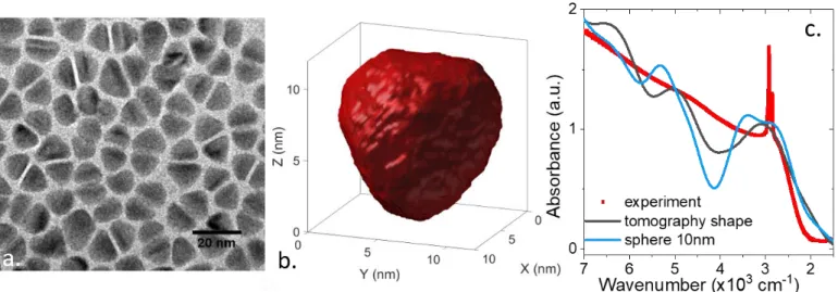
We start by growing narrow band gap nanocrystals (NCs) made of HgTe and PbS, see experimental section and supplementary information (figure S1-4) for details about syntheses, we focus on HgTe with a band gap in the extended SWIR (4000 cm-1 cut-off, later called HgTe 4k) and in mid wave infrared (2000 cm-1 cut-off, later called HgTe 2k). The particles are grown using the procedure of Keuleyan et al.46 The obtained particles are depicted in Figure 1. They present a slightly non spherical shape as revealed by transmission electron microscopy (TEM, see Figure 1) and better highlighted by electron tomography (Figure 1b and movie S1). In particular, a 3D reconstruction of the particle clearly shows facets. The absorption spectrum of the particles is given in Figure 1c and presents a cut-off at 2000 cm-1 (≈5 µm or ≈250 meV). To understand how the particle non sphericity impacts the absorption spectrum, the particle shape is used as the input of atomistic tight-binding simulations of the electronic structure. From these simulations we calculate the optical spectra using the Fermi Golden rule13,47,48. A comparison between the experimental spectrum and the one resulting from tomography and tight binding simulation is depicted in Figure 1c. We note that the band-edge energy and the slope at higher energies is well reproduced. For sake of comparison the spectrum obtained from a spherical shape particle including the same number of atoms as the one obtained from tomography is given in Figure 1c. On the sphere shape spectrum, the exciton appears as a double peak followed by a dip which is not observed experimentally. This dip has been recently shown49 from ensemble measurements on spherical nanocrystals. For this type of shape, which appears as a marginally reshaped sphere, the impact on the spectrum remains nevertheless smaller than the experimental broadening. On the other hand, it still may play a role in their collective behavior by affecting their packing, and thus the film mobility.
Figure 1 Structure of HgTe NCs and its impact on the electronic spectrum. a. TEM image of
the HgTe CQDs with a cut-off wavelength around 5 µm. c. 3D visualisation of a tomographic
reconstruction of an HgTe CQD with a cut-off wavelength around 5 µm.c. Infrared spectrum for HgTe
CQDs with a cut-off wavelength around 2000 cm
-1(≈5 µm or ≈250 meV). The narrow doublet at
2900 cm
-1corresponds to the C-H bond from the ligands. The simulated spectrum resulting from
tight binding simulations are also provided using the shape determined from tomography and using
a spherical shape (10 nm diameter) while keeping the total number of atoms (15400) constant.
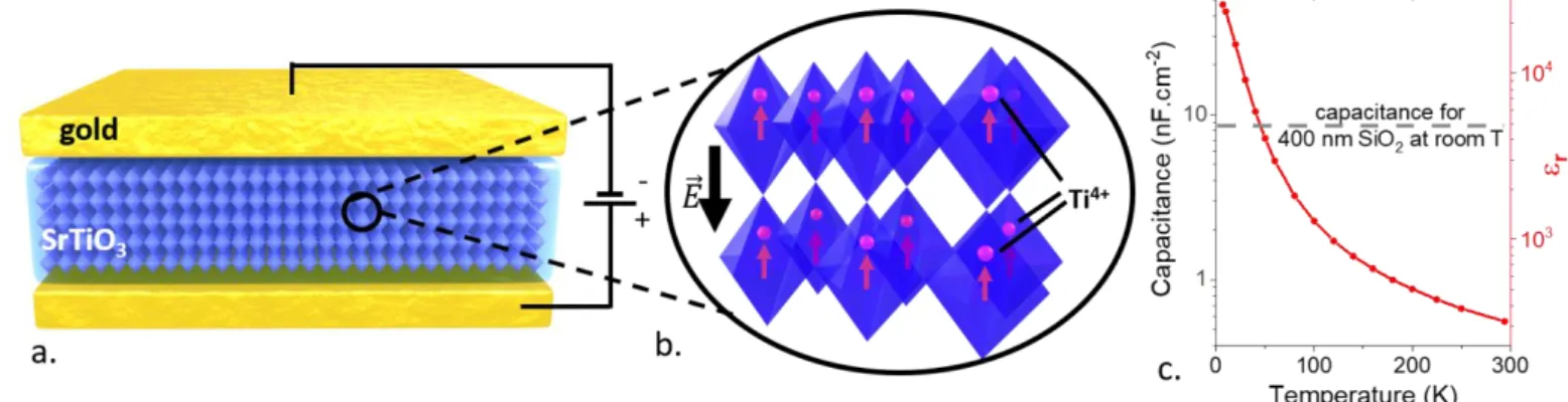
Before integrating the NCs into a FET, we confirm the ability of STO to lead to ultra-high dielectric constant. To do so, we design a capacitor from the STO substrate as depicted in Figure 2a. Using Atomic force microscopy, we check the quality of the STO surface which presents a low roughness (Figure S5) of the order of 1.4 nm which is much lower than the NC size (12 nm). Under bias application, the Ti4+ ions move from the center of the perovskite octahedrons (Figure 2b) leading to a polarization. The obtained capacitance and equivalent dielectric constant are given in Figure 2c. As it may have been anticipated, we see a clear rise of the dielectric constant as temperature is cooled, from 300 at room temperature up to 30 000 for low T (T≈10 K). In spite of the thick aspect of the substrate (500 µm thickness), capacitance larger than the one resulting from SiO2 can be obtained.
Figure 2 Principle of ferroelectric gating.a. Sketch of a capacitor based on STO as ferroelectric.
b. Zoom on the Ti based octahedron of the perosvkite material. As Ti ions move away from the
octahedron center, a polarization appears. c. Sheet capacitance and dielectric constant for the STO
substrate, later used as gate.
To confirm this promise, we then pattern the STO substrate with interdigitated electrodes using conventional optical lithography. A film of nanocrystals is then deposited and their native capping ligands are exchanged thanks to a phase transfer procedure proposed by Martinez et al.5 For sake of comparison, we also fabricate FETs based on the same nanocrystals using a SiO2 gate and an electrolyte gate. Sketches of the devices are shown in Figure 3a-c
Electrolyte due to the freezing of the ions can only be used near room temperature, see Figure 3d. Current modulation is lost for T lower than 280 K, see Figure S8. It also needs to be operated slowly, with a sweep rate ≈ 1 mV.s-1 to let time for ion diffusion (otherwise hysteresis becomes dramatically large). However, due to its large capacitance, electrolyte is the method which requires the lowest gate bias range (≈2 V). With SiO2 as dielectric, low temperature operation (Figure 3f and S8) and fast sweeping (Figure 3h) can be obtained. SiO2 gate is also the only gate not to present an hysteretic behavior in the tranfer curve, suggetsing that interface traps plays a reduced role contrary to the other gate method. However, in practice, even using SiO2 prepared with dry methods, sucess ratio to obtain unshorted devices remains far below 1 and electrical breakdowns are observed for fast sweep rate operation. This issue is fully solved using STO, the latter being a thick (500 µm) strongly insulating substrate, devices are unshorted and no breakdown through the dielectric is observed even under biases as high as 200 V. Note that not a single device has generated breakdown over this study, whatever the applied biases and sweep rates. This makes that STO is the gating strategy leading to the lowest leakage and so the highest drain/leakage current ratio. Even if it requires high operating biases, the power used to drive the gate remains low due to the low leakage current.
As expected from the temperature dependence of the dielectric constant, see Figure 2c, STO FET requires operation below 100 K (Above this temperature the current modulation gets very weak, see Figure S6 and S8) and the on/off ratio is maximal around 50 K, see Figure 3e,g and S8-9. We also verify that STO gating allows fast (ie with respect to electrolyte) sweeping of the gate bias, see Figure 3h. The mobility in this range of temperature is thermally activated and drops from a value of 10-2 cm2V-1s-1 around 100 K to 10-5 cm2V-1s-1 at 10 K. It is interesting to point that the mobilities obtained from STO are weaker, by a factor 10, than the ones measured from silica gates, see figure S10. Talapin’s group21 recently reported mobility values above 1 cm2.V-1s-1 for HgTe CQDs with the same band edge and similar surface chemistries. This suggests that the gate itself might be responsible for the reduced mobilities. As the gate dielectric constant is increased, the formation of Frohlich polarons50 coupling the charge within the QD to the polar vibration in the substrate is favored. This polaron formation and the higher interface traps density revealed by the hysteresis are responsible for the reduced mobilities. In spite of an higher hysteresis and a lower mobilities than SiO2, the STO gate remains interesting for the design of phototransistors, since this substrate is transparent in the visible and in the infrared enabling back side illumination for example which is not possible in the case of a Si/SiO2 wafer
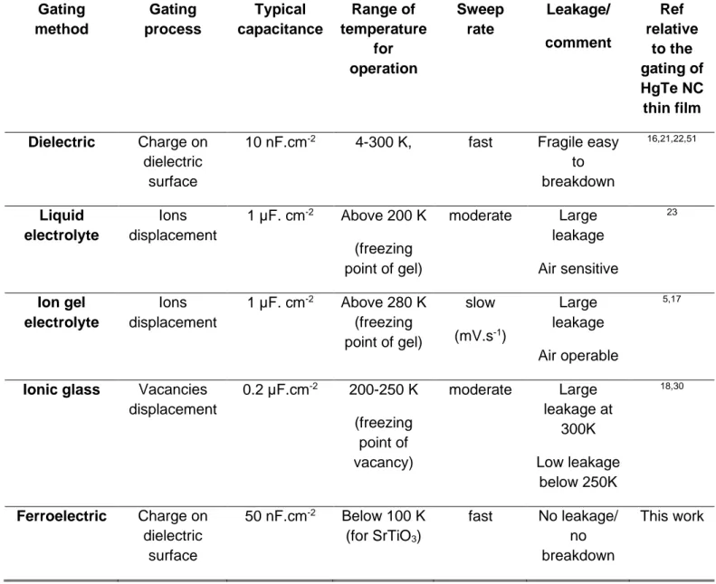
Table 1 summarizes the FET figures of merit for the different gate strategies. To further demonstrate the generality of the gating method, we apply STO gating to HgTe NCs with wider band gap (band-edge energy of 4000 cm-1 and 6500 cm-1, see Figure S2 and S3) as well as to other materials (PbS with band-edge of 6500 cm-1, see figure S4), see Figure S7.
Figure 3 Comparison of various gate technologies for narrow band gap NC-based FETs. a.
Sketch of a FET based on a HgTe CQD channel and where the gate is based on electrolyte. b.
Sketch of a FET based on a HgTe CQD channel and where the gate is based on ferroelectric STO.
c. Sketch of a FET based on a HgTe CQD channel and where the gate is based on dielectric SiO
2.
d-f are respectively the transfer curves (drain and gate current as a function of gate bias under
consant drain source bias) for electrolyte (T=300 K), STO (T=30 K) and SiO
2(T=30 K) gate based
FET which channel is made of HgTe 2k NCs. g. On/off ratio and electron mobility from the FET
transfer curves as a function of the temperature, for ferroelectric gate (ie STO). h. On/off ratio from
the FET transfer curves as a function of the sweep-rate for the different gates.
Table 1 figure of merit for different strategies of gating in field effect transistor based on
HgTe CQD as channel.
Gating method Gating process Typical capacitance Range of temperature for operation Sweep rate Leakage/ comment Ref relative to the gating of HgTe NC thin film Dielectric Charge on dielectric surface10 nF.cm-2 4-300 K, fast Fragile easy to breakdown 16,21,22,51 Liquid electrolyte Ions displacement 1 µF. cm-2 Above 200 K (freezing point of gel) moderate Large leakage Air sensitive 23 Ion gel electrolyte Ions displacement 1 µF. cm-2 Above 280 K (freezing point of gel) slow (mV.s-1) Large leakage Air operable 5,17
Ionic glass Vacancies displacement 0.2 µF.cm-2 200-250 K (freezing point of vacancy) moderate Large leakage at 300K Low leakage below 250K 18,30 Ferroelectric Charge on dielectric surface 50 nF.cm-2 Below 100 K (for SrTiO3) fast No leakage/ no breakdown This work
Even though relying on a thick substrate, (500 µm) the capacitance achieved by the STO (C≈50 nF.cm-2) corresponds to the one obtained for only 80 nm of SiO2, while being a breakdown free gating method. This result is even more promising given the recent developments relative to the growth of thin films of ferroelectric oxides.52–54 Such developments may lead to capacitances as high as the one of electrolyte without ion displacement. This makes this method highly promising for the design of FETs and phototransistors operated in cryogenic conditions.
Now that we have established the design of FET based on STO gate, we apply this strategy to the fabrication of a phototransistor. Gate effect is generally a surface effect and thus high performing FETs rely on this films which present a weak absorption. To overcome this difficulty, two strategies are possible increasing the film thickness55 or the control of the light matter coupling.56 Here, we focus on the latter strategy and show that a plasmonic resonance57–59 can be induced thanks to Guided Mode Resonators (GMRs).10,33 The GMRs rely on a grating which role is to transform the single pass of the light through the film into a propagating mode along the substrate enabling multiple passes of the light. While these methods have been applied to planar photoconductive and vertical photovoltaic devices60, its implementation on phototransistors has not been reported yet.
The GMR relies on a grating which period is proportional to ≈λ/n where λ is the resonance wavelength of the grating and n the optical index. Here we apply the method to HgTe 4k (2.5 µm cut-off wavelength) which leads to a period of 2 µm. This is typically 10 times smaller than the period of the conventional interdigitated
electrodes used in the first part of this paper. This period reduction has a dual benefit. First, it leads to enhanced absorption due to the introduction of the resonance. Secondly, the interelectrode spacing reduces the transit time as well (time required for charges to reach the opposite electrode) and generates some photoconductive gain, which further enhances the device responsivity. While GMR have been previously reported for infrared NCs devices,10,33,61 its implementation on STO substrate is more challenging because of the low optical index of STO (n ≈2.25).62,63 Compared to SiO2 substrate (n=1.44), the index mismatch between the NC film (n=1.9)64 and the substrate is drastically changed requiring an update of the geometrical parameters.
Figure 4 Design of Guided Mode Resonator onto a STO substrate. a. Scheme of the GMR
phototransistor based on a STO gate and a HgTe NCs channel. b. (resp. c.) Intensity of the
absorption in the TM mode at TM1 wavelength (resp. TE at TE1 wavelength). d. Simulated
absorption spectra in TM, TE and for unpolarized light. e. Simulated absorption spectra for a thin
and thick film of HgTe NCs on interdigitated electrodes and GMR phototransistor based on a STO
substrate.
A Sketch of the targeted structure is depicted in Figure 4a and details relative to design and fabrication provided in Figure S13-17 In addition, a gold back side mirror is deposited on the bottom of the STO substrate enabling a double pass of the light through the absorbing layer. Using RCWA simulations,65 we design a structure (i) where the first resonance, in TM mode (mode TM1 in Figure 4d), of the grating matches the material band edge. In addition (ii) we optimize the structure in order that the TE resonance (mode TE1 in Figure 4d) and the second order from TM mode (mode TM2 in Figure 4d) induce additional resonances in the short-wave infrared to obtain a broad band enhancement of the light absorption. Last (iii), we also take great care to localize the absorption within the HgTe absorbing layer rather that in the gold contacts which would lead to thermal losses, see the electromagnetic absorption map in Figure 4b and c. Here, 85% of the light absorption is occurring within the NC film.
The added value of the GMR electrodes is clearly highlighted in Figure 4e. Using a thin film (80 nm, typical for traditional FET) of HgTe NCs only 2% of the incident light is absorbed at the band edge. Here, the use of large capacitance gate allows the increase the absorbing NC film thickness (310 nm). The film thickness increase enhances the absorption up to 10% of the incident light at the band edge. Once GMR are introduced, a broad band absorption close to 30% is achieved in the whole SWIR and extended SWIR regions, see Figure 4e. This corresponds to a 15 times enhancement of the light absorption compared to a traditional FET design.
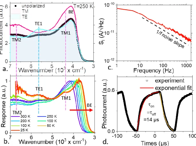
Figure 5 presents the characterization of the device relying on GMR electrodes. The spectral photoresponse (Figure 5a) shows a polarized response, with a TE mode appearing between the two TM contributions. Experimental data appears slightly redshifted and broader than the simulated spectrum from Figure 4d. We attribute this discrepancy to the poor evaluation of the real part of the optical index of the NC film (taken as a spectrally constant value of 1.9, see Figure S11 to see the effect of the real part of HgTe NCs film onto the GMR absorption spectrum). Future work will have to be dedicated to a more accurate determination of the complex optical index of this film.
Temperature dependence of the spectrum (Figure 5b) can further confirms the different origin of the feature observed in the absorption spectrum. We clearly see that the energy peaks resulting from the grating (TM1 and 2 as well as TE1) are temperature independent in agreement with the fact that their energy is driven by geometrical factors. On the other hand, the band-edge redshifts which is consistent with previous observation for HgTe NCs presenting a positive value for dEG/dT=190 µeV.K-1.66,67
The reduction of the electrode spacing period from 20 µm to ≈2 µm increases the photoconductive gain. The latter can be estimated using the expression 𝑔 =𝑅
𝜂 𝑒
ℎ𝑣, with R the responsivity, 𝜂 the device absorption, e the
proton charge and ℎ𝑣 the incident photon energy. The gain in presence of the GMR is estimated to be 0.1, below unity indicating that the photocarrier diffusion length remains much smaller than the inter electrode spacing. Overall, the introduction of the GMR electrodes increases the photoresponse by a factor 33, as shown in Figure S17. The latter decomposed over a factor 3 for the absorption enhancement (for same film thickness) and factor ≈10 due to electrical gain.
Figure 5 Detection properties of the GMR electrodes. a. Experimental photocurrent spectra in
TM, TE and for unpolarized light at 250 K. b. Temperature evolution of the photocurrent spectra of
GMR phototransistor based on STO. c. Noise current specral density for the GMR based device.
The blackline depicts the slope expected for 1/f noise. d. Photocurrent as a function of time as a
laser source at 1.55 µm is turned on and off. For all graphs of this figure the gate is floating.
The noise in this device is found to be 1/f limited,68,69 see Figure 5c. While the gate is floating, at 30 K and for 1 kHz signal, the detectivity has been evaluated to be 1.6x10⁸ Jones, mostly limited by the drop of the mobility value at low temperature. The response time of the device is 14 µs, see Figure 5d, fully compatible with most IR imaging applications.
To finish, we test the potential of the combination of STO gate with the GMR electrode. Thanks to the large capacitance of the gate, the gate effect remains effective on a film as thick as 310 nm and we observed a 5 orders of magnitude modulation of the dark current, see Figure 6. Similarly, the responsivity appears to be gate dependent. Its maximum value reaches 150 mA.W-1, which clearly benefit from the GMR electrodes (same film on non-GMR electrodes, under same gate bias, presents a maximum responsivity of 4.5 mA.W-1, see Figure S16). As a result, the gate can be used to shift the device operating point and we found that -50 V leads to an enhancement of the signal to noise ratio by a factor 12 000, which corresponds to a detectivity as high as 1.9x10¹² Jones, for 30 K operation at 1 kHz, and for 3 µm cut-off detection. This low temperature operation enables to obtain the ultimate performance of the material and corresponds to the largest detectivity value reported for HgTe NCs operating in the extended SWIR even though it is at the price of a strong cryogenic cooling.
Figure 6 Phototransistor combining GMR electrodes and STO gate. Dark current, responsivity
and normalized ratio (by value at V
GS=0V) of the responsivity of over the dark current as a function
of the gate bias for the GMR device.
In summary, we have demonstrated a new type of gate for nanocrystal films relying on STO ferroelectric gating which is fully compatible with low T operation. Thanks to a dielectric constant as large as 30 000, breakdown free, leakage free gating of nanocrystal film is demonstrated and can be applied to a broad range of materials. This result is highly promising with the development of thin film growth of ferroelectric materials which will allow to tune the Curie temperature and expand these results in the whole 4 K and 300 K temperature range of operation. This will certainly raise new material challenges. Even though pulsed laser deposition is currently the most used strategies to grow such ferroelectric oxides, this method is not compatible with high throughput neither with large scale deposition. Thus, further progresses relative to atomic layer deposition of oxides may offer an interesting alternative. We then address a key limitation of phototransistors, which was their low absorption. We introduce a plasmonic resonator based on GMR. The design is made to obtain three distinct resonances enabling broad band enhancement of the absorption from 1.5 to 3 µm. The introduction of the resonators enhances the light absorption by a factor 15 compared to conventional transistor geometry and also leads to electrical gain. Because we combine gate effect and strong absorption, we identify an optimal operating condition, for this 3 µm cut-off wavelength detector, which detectivity is above 1012 Jones for 30 K operation.
Methods
Chemicals for nanocrystal synthesis. Mercury chloride (HgCl2, Strem Chemicals, 99%), tellurium powder (Te, Sigma-Aldrich, 99.99%), trioctylphosphine (TOP, Cytek, 90%), oleylamine (OLA, Acros, 80-90%), dodecanethiol (DDT, Sigma-Aldrich, 98%), lead chloride (PbCl2, Alfa Aesar, 99%), sulfur powder (S, Alfa Aesar, 99.5%), oleic acid (OA, Alfa Aesar, 90%), 1,2,ethanedithiol (EDT, Fluka, 98.0%), lithium perchlorate (LiClO4, Sigma-Aldrich, 98%), polyethylene glycol (PEG, Mw = 6 kg.mol-1), chloroform (VWR), ethanol absolute anhydrous (VWR), methanol (Carlo Erba, 99.8%), acetone (VWR), n-hexane (VWR), toluene (Carlo Erba, 99.3%), N,N-dimethylformamide (DMF, Sigma Aldrich), mercaptoethanol (MpOH, Merck, >99%),
Methylisobutylketone (MIBK, VWR, >98.5 %). All chemicals are used as received. Mercury and lead salts are toxic, handle them with great care.
1 M TOP:Te precursor: In a three-neck flask, 2.54 g of Te powder is mixed in 20 mL of TOP. The flask is kept under vacuum at room temperature for 5 min and then is heated up to 100 °C and kept under vacuum for 20 more minutes. The atmosphere is changed to N2 and the temperature is raised to 275 °C. The solution is stirred until a clear orange coloration is obtained. Then the flask is cooled down and the color switches to yellow. The flask is degassed again for 10 min at room temperature. This solution is finally transferred to an N2-filled glovebox for storage.
HgTe CQD synthesis with band edge at 2000 cm-1: The reaction is taken from Keuleyan et al.46 510 mg of HgCl2 was added to 60 mL of oleylamine in a 100 mL round flask. The solution was placed under vacuum and heated to 110 °C for 1 h. Then, the temperature is increased to 120 °C and solution placed to N2 atmosphere. 1.9 mL of TOP:Te (1 M) with 10 mL of oleylamine are added to the mercury solution. The solution color gradually turns to dark brown and the reaction is stopped at 3 min. A solution made of 1 mL of dodecanethiol and 9 mL of toluene is quickly added to quench the reaction. The nanocrystals are then precipitated with ethanol. After centrifugation, the nanocrystals are redispersed in chloroform. The washing step is repeated one more time. Synthesis for other band edge energies and other material are given in the SI
Liquid state ligand exchange: Ligand exchange solution is prepared as followed: 15 mg of HgCl2 are dissolved in 9 mL of DMF, then 1 mL of mercaptoethanol is added. This solution is then used to prepare a concentrated ink. 500 µL of NC solution at 50 mg.mL-1 is mixed with 6 mL of hexane. 1 mL of ligand exchange solution is added and mixed vigorously. NCs phase transfer is observed from the apolar phase to the polar phase. The apolar phase is removed and another 6 mL of hexane is added to perform a second cleaning. At this step 500 µL of fresh DMF is added. The apolar phase is removed and another cleaning step is performed. Few drops of EtOH are added and the NCs are precipitated. Finally they are redispersed in DMF at a concentration of ≈160 mg.mL-1.
Film deposition. 15 µL of ink solution is spin-coated of the substrate at 3000 rpm for 60 s to get a thin film (<100 nm). For thicker film spin-coating is performed at 1300 rpm for 200 s before a drying step at 2500 rpm for 120 s.
Transport and optoelectronic characterization. Procedures relative to electronic transport (FET characterization) and optoelectronic measurements (spectral response, responsivity, noise, detectivity) are given in the supporting information and more specially in Figure S11-12.
Infrared spectroscopy is conducted using a Fisher IS50 Fourier transform Infrared spectrometer. The visible light source is used. To measure CQD absorption, we use the spectrometer in ATR configuration. A drop of CQD solution is dried on the diamond cell. The source is a white light and the detector is a DTGS ATR. Spectra are typically acquired between 10000 cm-1 and 2000 cm-1 with a 4 cm-1 resolution and averaging over 32 spectra. To measure a film absorption, an extended InGaAs detector is used and the source is a white light. In case of extended SWIR device, the visible light is switch to a glow bar source combined with a DTGS detector. Each spectrum is averaged 32 times and the resolution is set to 4 cm-1. Photocurrent spectra are acquired as the sample is biased using a Femto DLPCA current amplifier which role is also to magnify the current. The signal is then fed into the FTIR acquisition board.
For TEM pictures, a drop of a diluted CQD solution is drop-casted on a copper grid covered with an amorphous carbon film. JEOL 2010F is used at 200 kV for acquisition of picture. For device characterization, a FEI Magellan scanning electron microscope is used.
Electron tomography: Electron tomography of single nanocrystal was performed using a FEI Tecnai Osiris electron microscope operating at 200 kV. A tilt series of high-angle annular dark-field transmission electron microscopy (HAADF-STEM) images were acquired from -75° to 69°, with a tilt increment of 3°. The projection images served as input for the 3D reconstruction performed through 20 iterations of the expectation maximization (EM) algorithm68 implemented in the ASTRA toolbox.69 The resulting 3D reconstruction was then segmented by defining a threshold value using Amira 5.4.0. The volume was extracted in a form of a 3D matrix used as input for the tight binding simulation.
Tight binding simulations: We used the tight binding model of Ref 47 to calculate the electronic structure of the HgTe NCs. Each Hg or Te atom is described by a double set of sp3d5s* orbitals, one for each spin orientation. Surfaces are saturated by pseudo-hydrogen atoms characterized by a single s orbital. Tight-binding parameters, i.e., on-site energies, nearest-neighbor hopping matrix elements and spin-orbit coupling terms were determined to provide a very good description of the band structure of bulk HgTe (at 300K). For the NC analyzed with electron tomography, we considered all atoms positioned on the zinc-blende lattice and included in the NC volume (15406 atoms). For all NCs, we calculated 60 (1200) conduction (valence) states and we computed dipolar matrix elements between them as described in Ref47. For comparison with experiments, the transition peaks are broadened by Gaussians of full width at half maximum of 41 meV Electromagnetic simulations: Calculations have been achieved with Matlab library based on Rigorous Coupled-Wave Analysis (RCWA).65 We considered incoming plane wave under normal incidence, either with transverse magnetic (TM) or transverse electric (TE) polarization, i.e. with magnetic field or electric field parallel with the slits of the gratings, respectively. Grating is supposed to be invariant along y direction and repeated infinitely along x direction.
Supporting Information
The Supporting Information is available free of charge at.
The Supporting Information includes additional information regarding: 1. Nanocrystal synthesis, 1.1. Nanocrystal synthesis. 2. Transport measurements, 2.1. Transistor measurements, 2.2. Optoelectronic characterization. 3. Guided Mode Resonator, 3.1. Electromagnetic simulations, 3.2. Complex optical index, 3.3. Effect of the thickness, 3.4. Dispersion diagram, 3.5. GMR electrode fabrication, 3.6. Comparison with regular electrodes
Author information Corresponding author
ACKNOWLEDEGMENTS
The project is supported by ERC starting grant blackQD (grant n° 756225) and consolidator grant Realnano (815128). This project has received funding from the European Commission (grant 731019, EUSMI). We acknowledge the use of clean-room facilities from the “Centrale de Proximité Paris-Centre”. This work has been supported by the Region Ile-de-France in the framework of DIM Nano-K (grant dopQD). This work was supported by French state funds managed by the ANR within the Investissements d'Avenir programme under reference ANR-11-IDEX-0004-02, and more specifically within the framework of the Cluster of Excellence MATISSE and also by the grant grant IPER-Nano2 (ANR-18CE30-0023-01), Copin (ANR-19-CE24-0022), Frontal (ANR-19-CE09-0017), Graskop (ANR-19-CE09-0026) and NITQuantum. JQ thanks Chinese Scholarship Council for PhD grant, while AC thanks Agence innovation defense.
REFERENCES
(1) Lu, H.; Carroll, G. M.; Neale, N. R.; Beard, M. C. Infrared Quantum Dots: Progress, Challenges, and Opportunities.
ACS Nano 2019, 13, 939–953.
(2) Hafiz, S. B.; Scimeca, M.; Sahu, A.; Ko, D.-K. Colloidal Quantum Dots for Thermal Infrared Sensing and Imaging.
Nano Converg. 2019, 6, 7.
(3) Lhuillier, E.; Guyot-Sionnest, P. Recent Progresses in Mid Infrared Nanocrystal Optoelectronics. IEEE J. Sel. Top.
Quantum Electron. 2017, 23, 6000208.
(4) McDonald, S. A.; Konstantatos, G.; Zhang, S.; Cyr, P. W.; Klem, E. J. D.; Levina, L.; Sargent, E. H. Solution-Processed PbS Quantum Dot Infrared Photodetectors and Photovoltaics. Nat. Mater. 2005, 4, 138–142. (5) Martinez, B.; Ramade, J.; Livache, C.; Goubet, N.; Chu, A.; Gréboval, C.; Qu, J.; Watkins, W. L.; Becerra, L.;
Dandeu, E.; et al. HgTe Nanocrystal Inks for Extended Short-Wave Infrared Detection. Adv. Opt. Mater. 2019,
7, 1900348.
(6) Tang, X.; Ackerman, M. M.; Chen, M.; Guyot-Sionnest, P. Dual-Band Infrared Imaging Using Stacked Colloidal Quantum Dot Photodiodes. Nat. Photonics 2019 2019, 13, 277–282.
(7) Tang, X.; Tang, X.; Lai, K. W. C. Scalable Fabrication of Infrared Detectors with Multispectral Photoresponse Based on Patterned Colloidal Quantum Dot Films. ACS Photonics 2016, 3, 2396–2404.
(8) Lhuillier, E.; Robin, A.; Ithurria, S.; Aubin, H.; Dubertret, B. Electrolyte-Gated Colloidal Nanoplatelets-Based Phototransistor and Its Use for Bicolor Detection. Nano Lett. 2014, 14, 2715–2719.
(9) Tang, X.; Ackerman, M. M.; Guyot‐Sionnest, P. Acquisition of Hyperspectral Data with Colloidal Quantum Dots.
Laser Photonics Rev. 2019, 13, 1900165.
(10) Chu, A.; Gréboval, C.; Goubet, N.; Martinez, B.; Livache, C.; Qu, J.; Rastogi, P.; Bresciani, F. A.; Prado, Y.; Suffit, S.; et al. Near Unity Absorption in Nanocrystal Based Short Wave Infrared Photodetectors Using Guided Mode Resonators. ACS Photonics 2019, 6, 2553–2561.
(11) Zhu, B.; Chen, M.; Zhu, Q.; Zhou, G.; Abdelazim, N. M.; Zhou, W.; Kershaw, S. V.; Rogach, A. L.; Zhao, N.; Tsang, H. K. Integrated Plasmonic Infrared Photodetector Based on Colloidal HgTe Quantum Dots. Adv. Mater. Technol. 2019, 4, 1900354.
(12) Chu, A.; Martinez, B.; Ferré, S.; Noguier, V.; Gréboval, C.; Livache, C.; Qu, J.; Prado, Y.; Casaretto, N.; Goubet, N.; et al. HgTe Nanocrystals for SWIR Detection and Their Integration up to the Focal Plane Array. ACS Appl.
Mater. Interfaces 2019, 11, 33116–33123.
(13) Keuleyan, S. E.; Guyot-Sionnest, P.; Delerue, C.; Allan, G. Mercury Telluride Colloidal Quantum Dots: Electronic Structure, Size-Dependent Spectra, and Photocurrent Detection up to 12 µm. ACS Nano 2014, 8, 8676–8682. (14) Lhuillier, E.; Scarafagio, M.; Hease, P.; Nadal, B.; Aubin, H.; Xu, X. Z.; Lequeux, N.; Patriarche, G.; Ithurria, S.;
Dubertret, B. Infrared Photodetection Based on Colloidal Quantum-Dot Films with High Mobility and Optical Absorption up to THz. Nano Lett. 2016, 16, 1282–1286.
(15) Goubet, N.; Jagtap, A.; Livache, C.; Martinez, B.; Portalès, H.; Xu, X. Z.; Lobo, R. P. S. M.; Dubertret, B.; Lhuillier, E. Terahertz HgTe Nanocrystals: Beyond Confinement. J. Am. Chem. Soc. 2018, 140, 5033–5036.
(16) Chen, M.; Lu, H.; Abdelazim, N. M.; Zhu, Y.; Wang, Z.; Ren, W.; Kershaw, S. V.; Rogach, A. L.; Zhao, N. Mercury Telluride Quantum Dot Based Phototransistor Enabling High-Sensitivity Room-Temperature Photodetection at 2000 Nm. ACS Nano 2017, 11, 5614–5622.
(17) Livache, C.; Izquierdo, E.; Martinez, B.; Dufour, M.; Pierucci, D.; Keuleyan, S.; Cruguel, H.; Becerra, L.; Fave, J. L.; Aubin, H.; et al. Charge Dynamics and Optolectronic Properties in HgTe Colloidal Quantum Wells. Nano Lett. 2017, 17, 4067–4074.
(18) Noumbé, U. N.; Gréboval, C.; Livache, C.; Chu, A.; Majjad, H.; Parra López, L. E.; Mouafo, L. D. N.; Doudin, B.; Berciaud, S.; Chaste, J.; et al. Reconfigurable 2D/0D p–n Graphene/HgTe Nanocrystal Heterostructure for Infrared Detection. ACS Nano 2020, 14, 4567–4576.
(19) Dong, Y.; Chen, M.; Yiu, W. K.; Zhu, Q.; Zhou, G.; Kershaw, S. V.; Ke, N.; Wong, C. P.; Rogach, A. L.; Zhao, N. Solution Processed Hybrid Polymer: HgTe Quantum Dot Phototransistor with High Sensitivity and Fast Infrared Response up to 2400 nm at Room Temperature. Adv. Sci. 2020, 7, 2000068.
(20) Talapin, D. V.; Murray, C. B. PbSe Nanocrystal Solids for n- and p-Channel Thin Film Field-Effect Transistors.
Science 2005, 310, 86–89.
(21) Lan, X.; Chen, M.; Hudson, M. H.; Kamysbayev, V.; Wang, Y.; Guyot-Sionnest, P.; Talapin, D. V. Quantum Dot Solids Showing State-Resolved Band-like Transport. Nat. Mater. 2020, 19, 323–329.
(22) Lhuillier, E.; Keuleyan, S.; Zolotavin, P.; Guyot‐Sionnest, P. Mid-Infrared HgTe/As2S3 Field Effect Transistors and Photodetectors. Adv. Mater. 2013, 25, 137–141.
(23) Liu, H.; Keuleyan, S.; Guyot-Sionnest, P. n- and p-Type HgTe Quantum Dot Films. J. Phys. Chem. C 2012, 116, 1344–1349.
(24) Lhuillier, E.; Ithurria, S.; Descamps-Mandine, A.; Douillard, T.; Castaing, R.; Xu, X. Z.; Taberna, P. L.; Simon, P.; Aubin, H.; Dubertret, B. Investigating the n- and p-Type Electrolytic Charging of Colloidal Nanoplatelets. J. Phys.
Chem. C 2015, 119, 21795–21799.
(25) Bisri, S. Z.; Piliego, C.; Yarema, M.; Heiss, W.; Loi, M. A. Low Driving Voltage and High Mobility Ambipolar Field-Effect Transistors with PbS Colloidal Nanocrystals. Adv. Mater. 2013, 25, 4309–4314.
(26) Balazs, D. M.; Bijlsma, K. I.; Fang, H.-H.; Dirin, D. N.; Döbeli, M.; Kovalenko, M. V.; Loi, M. A. Stoichiometric Control of the Density of States in PbS Colloidal Quantum Dot Solids. Sci. Adv. 2017, 3, eaao1558.
(27) Liu, L.; Bisri, S. Z.; Ishida, Y.; Hashizume, D.; Aida, T.; Iwasa, Y. Ligand and Solvent Effects on Hole Transport in Colloidal Quantum Dot Assemblies for Electronic Devices. ACS Appl. Nano Mater. 2018, 1, 5217–5225.
(28) Miranti, R.; Shin, D.; Septianto, R. D.; Ibáñez, M.; Kovalenko, M. V.; Matsushita, N.; Iwasa, Y.; Bisri, S. Z. Exclusive Electron Transport in Core@Shell PbTe@PbS Colloidal Semiconductor Nanocrystal Assemblies. ACS Nano 2020,
14, 3242–3250.
(29) Septianto, R. D.; Liu, L.; Iskandar, F.; Matsushita, N.; Iwasa, Y.; Bisri, S. Z. On-Demand Tuning of Charge Accumulation and Carrier Mobility in Quantum Dot Solids for Electron Transport and Energy Storage Devices.
NPG Asia Mater. 2020, 12, 33.
(30) Gréboval, C.; Noumbe, U.; Goubet, N.; Livache, C.; Ramade, J.; Qu, J.; Chu, A.; Martinez, B.; Prado, Y.; Ithurria, S.; et al. Field-Effect Transistor and Photo-Transistor of Narrow-Band-Gap Nanocrystal Arrays Using Ionic Glasses. Nano Lett. 2019, 19, 3981–3986.
(31) Biscaras, J.; Chen, Z.; Paradisi, A.; Shukla, A. Onset of Two-Dimensional Superconductivity in Space Charge Doped Few-Layer Molybdenum Disulfide. Nat. Commun. 2015, 6, 8826.
(32) Paradisi, A.; Biscaras, J.; Shukla, A. Space Charge Induced Electrostatic Doping of Two-Dimensional Materials: Graphene as a Case Study. Appl. Phys. Lett. 2015, 107, 143103.
(33) Rastogi, P.; Chu, A.; Gréboval, C.; Qu, J.; Noumbé, U. N.; Chee, S.-S.; Goyal, M.; Khalili, A.; Xu, X. Z.; Cruguel, H.; et al. Pushing Absorption of Perovskite Nanocrystals into the Infrared. Nano Lett. 2020, 20, 3999–4006. (34) Kahmann, S.; Shulga, A.; Loi, M. A. Quantum Dot Light-Emitting Transistors—Powerful Research Tools and Their
Future Applications. Adv. Funct. Mater. 2020, 30, 1904174.
(35) Kim, D. K.; Lai, Y.; Diroll, B. T.; Murray, C. B.; Kagan, C. R. Flexible and Low-Voltage Integrated Circuits Constructed from High-Performance Nanocrystal Transistors. Nat. Commun. 2012, 3, 1216.
(36) Dolzhnikov, D. S.; Zhang, H.; Jang, J.; Son, J. S.; Panthani, M. G.; Shibata, T.; Chattopadhyay, S.; Talapin, D. V. Composition-Matched Molecular “Solders” for Semiconductors. Science 2015, 347, 425–428.
(37) Chung, D. S.; Lee, J. S.; Huang, J.; Nag, A.; Ithurria, S.; Talapin, D. V. Low Voltage, Hysteresis Free, and High Mobility Transistors from All-Inorganic Colloidal Nanocrystals. Nano Lett. 2012, 12, 1813–1820.
(38) Nugraha, M. I.; Häusermann, R.; Watanabe, S.; Matsui, H.; Sytnyk, M.; Heiss, W.; Takeya, J.; Loi, M. A. Broadening of Distribution of Trap States in PbS Quantum Dot Field-Effect Transistors with High-k Dielectrics.
ACS Appl. Mater. Interfaces 2017, 9, 4719–4724.
(39) Shulga, A. G.; Piveteau, L.; Bisri, S. Z.; Kovalenko, M. V.; Loi, M. A. Double Gate PbS Quantum Dot Field-Effect Transistors for Tuneable Electrical Characteristics. Adv. Electron. Mater. 2016, 2, 1500467.
(40) Biscaras, J.; Hurand, S.; Feuillet-Palma, C.; Rastogi, A.; Budhani, R. C.; Reyren, N.; Lesne, E.; Lesueur, J.; Bergeal, N. Limit of the Electrostatic Doping in Two-Dimensional Electron Gases of LaXO3 (X = Al, Ti)/SrTiO3. Sci. Rep. 2014, 4, 6788.
(41) Hurand, S.; Jouan, A.; Feuillet-Palma, C.; Singh, G.; Biscaras, J.; Lesne, E.; Reyren, N.; Barthélémy, A.; Bibes, M.; Villegas, J. E.; et al. Field-Effect Control of Superconductivity and Rashba Spin-Orbit Coupling in Top-Gated LaAlO3/SrTiO3 Devices. Sci. Rep. 2015, 5, 12751.
(42) Biscaras, J.; Bergeal, N.; Hurand, S.; Grossetête, C.; Rastogi, A.; Budhani, R. C.; LeBoeuf, D.; Proust, C.; Lesueur, J. Two-Dimensional Superconducting Phase in LaTiO3/SrTiO3 Heterostructures Induced by High-Mobility Carrier Doping. Phys. Rev. Lett. 2012, 108, 247004.
(43) Caviglia, A. D.; Gariglio, S.; Reyren, N.; Jaccard, D.; Schneider, T.; Gabay, M.; Thiel, S.; Hammerl, G.; Mannhart, J.; Triscone, J.-M. Electric Field Control of the LaAlO3 /SrTiO3 Interface Ground State. Nature 2008, 456, 624– 627.
(44) Chen, S.; Ruiter, R.; Mathkar, V.; Wees, B. J. van; Banerjee, T. Temperature and Electric Field Dependence of Spin Relaxation in Graphene on SrTiO3. Phys. Status Solidi RRL – Rapid Res. Lett. 2018, 12, 1800216.
(45) Shahnazaryan, V.; Kyriienko, O.; Rostami, H. Exciton Routing in the Heterostructure of a Transition Metal Dichalcogenide Monolayer on a Paraelectric Substrate. Phys. Rev. B 2019, 100, 165303.
(46) Keuleyan, S.; Lhuillier, E.; Guyot-Sionnest, P. Synthesis of Colloidal HgTe Quantum Dots for Narrow Mid-IR Emission and Detection. J. Am. Chem. Soc. 2011, 133, 16422–16424.
(47) Allan, G.; Delerue, C. Tight-Binding Calculations of the Optical Properties of HgTe Nanocrystals. Phys. Rev. B -
Condens. Matter Mater. Phys. 2012, 86, 165437.
(48) Hudson, M. H.; Chen, M.; Kamysbayev, V.; Janke, E. M.; Lan, X.; Allan, G.; Delerue, C.; Lee, B.; Guyot-Sionnest, P.; Talapin, D. V. Conduction Band Fine Structure in Colloidal HgTe Quantum Dots. ACS Nano 2018, 12, 9397– 9404.
(49) Zhang, H.; Guyot-Sionnest, P. Shape-Controlled HgTe Colloidal Quantum Dots and Reduced Spin–Orbit Splitting in the Tetrahedral Shape. J. Phys. Chem. Lett. 2020, 11, 6860–6866.
(50) Hulea, I. N.; Fratini, S.; Xie, H.; Mulder, C. L.; Iossad, N. N.; Rastelli, G.; Ciuchi, S.; Morpurgo, A. F. Tunable Fröhlich Polarons in Organic Single-Crystal Transistors. Nat. Mater. 2006, 5, 982–986.
(51) Chen, M.; Lan, X.; Tang, X.; Wang, Y.; Hudson, M. H.; Talapin, D. V.; Guyot-Sionnest, P. High Carrier Mobility in HgTe Quantum Dot Solids Improves Mid-IR Photodetectors. ACS Photonics 2019, 6, 2358–2365.
(52) Zarubin, S.; Suvorova, E.; Spiridonov, M.; Negrov, D.; Chernikova, A.; Markeev, A.; Zenkevich, A. Fully ALD-Grown TiN/Hf0.5Zr0.5O2/TiN Stacks: Ferroelectric and Structural Properties. Appl. Phys. Lett. 2016, 109, 192903. (53) Everhardt, A. S.; Denneulin, T.; Grünebohm, A.; Shao, Y.-T.; Ondrejkovic, P.; Zhou, S.; Domingo, N.; Catalan, G.; Hlinka, J.; Zuo, J.-M.; et al. Temperature-Independent Giant Dielectric Response in Transitional BaTiO3 Thin Films. Appl. Phys. Rev. 2020, 7, 011402.
(54) Strnad, N. A.; Potrepka, D. M.; Pulskamp, J. S.; Liu, Y.; Jones, J. L.; Phaneuf, R. J.; Polcawich, R. G. Texture and Phase Variation of ALD PbTiO3 Films Crystallized by Rapid Thermal Anneal. J. Vac. Sci. Technol. A 2019, 37, 020917.
(55) Fan, J. Z.; Vafaie, M.; Bertens, K.; Sytnyk, M.; Pina, J. M.; Sagar, L. K.; Ouellette, O.; Proppe, A. H.; Rasouli, A. S.; Gao, Y.; et al. Micron Thick Colloidal Quantum Dot Solids. Nano Lett. 2020, 20, 5284–5291.
(56) Baek, S.-W.; Molet, P.; Choi, M.-J.; Biondi, M.; Ouellette, O.; Fan, J.; Hoogland, S.; Arquer, F. P. G. de; Mihi, A.; Sargent, E. H. Nanostructured Back Reflectors for Efficient Colloidal Quantum-Dot Infrared Optoelectronics.
Adv. Mater. 2019, 31, 1901745.
(57) Tang, X.; fu Wu, G.; Lai, K. W. C. Plasmon Resonance Enhanced Colloidal HgSe Quantum Dot Filterless Narrowband Photodetectors for Mid-Wave Infrared. J. Mater. Chem. C 2017, 5, 362–369.
(58) Chen, M.; Shao, L.; Kershaw, S. V.; Yu, H.; Wang, J.; Rogach, A. L.; Zhao, N. Photocurrent Enhancement of HgTe Quantum Dot Photodiodes by Plasmonic Gold Nanorod Structures. ACS Nano 2014, 8, 8208–8216.
(59) Yifat, Y.; Ackerman, M.; Guyot-Sionnest, P. Mid-IR Colloidal Quantum Dot Detectors Enhanced by Optical Nano-Antennas. Appl. Phys. Lett. 2017, 110, 041106.
(60) Tang, X.; Ackerman, M. M.; Guyot-Sionnest, P. Thermal Imaging with Plasmon Resonance Enhanced HgTe Colloidal Quantum Dot Photovoltaic Devices. ACS Nano 2018, 12, 7362–7370.
(61) Tang, X.; Ackerman, M. M.; Shen, G.; Guyot-Sionnest, P. Towards Infrared Electronic Eyes: Flexible Colloidal Quantum Dot Photovoltaic Detectors Enhanced by Resonant Cavity. Small 2019, 15, 1804920.
(62) Weber, M. J. Volume IV: OPTICAL MATERIALS, p. 100. In Handbook of optical materials; CRC Press: Boca Raton, 2003.
(63) Driscoll, W. G.; Vaughan, W.; Optical Society of America. P. 7. In Handbook of optics; McGraw-Hill: New York, 1978.
(64) When Re(n) Increases, Both TE and TM Peaks Are Redshifted. For Low Re(n), the FWHM of TE Peak Decreases Due to the Perturbation Induced by the Apparition of the Diffraction Peak in Air at 2 µm, See Figure S13b. In the Rest of the Paper, Re(n)=1.9 Is Chosen as a Trade-off between the Width of the TE Peak and the Redshift of the TM Peak.
(65) Hugonin, J.-P.; Lalanne, P. Reticolo Software for Grating Analysis. Reticolo Softw. Grating Anal. Inst. D’Optique
(66) Lhuillier, E.; Keuleyan, S.; Guyot-Sionnest, P. Optical Properties of HgTe Colloidal Quantum Dots.
Nanotechnology 2012, 23, 175705.
(67) Moghaddam, N.; Gréboval, C.; Qu, J.; Chu, A.; Rastogi, P.; Livache, C.; Khalili, A.; Xu, X. Z.; Baptiste, B.; Klotz, S.; et al. The Strong Confinement Regime in HgTe Two-Dimensional Nanoplatelets. J. Phys. Chem. C 2020, 124, 23460–23468.
(68) Moon, T. K. The Expectation-Maximization Algorithm. IEEE Signal Process. Mag. 1996, 13, 47–60.
(69) van Aarle, W.; Palenstijn, W. J.; De Beenhouwer, J.; Altantzis, T.; Bals, S.; Batenburg, K. J.; Sijbers, J. The ASTRA Toolbox: A Platform for Advanced Algorithm Development in Electron Tomography. Ultramicroscopy 2015, 157, 35–47.