HAL Id: hal-03083265
https://hal.archives-ouvertes.fr/hal-03083265
Submitted on 18 Dec 2020
HAL is a multi-disciplinary open access
archive for the deposit and dissemination of
sci-entific research documents, whether they are
pub-lished or not. The documents may come from
teaching and research institutions in France or
abroad, or from public or private research centers.
L’archive ouverte pluridisciplinaire HAL, est
destinée au dépôt et à la diffusion de documents
scientifiques de niveau recherche, publiés ou non,
émanant des établissements d’enseignement et de
recherche français ou étrangers, des laboratoires
publics ou privés.
Design Methodology and Timing Considerations for
Implementing a TDC on a Cyclone V FPGA Target
Wassim Khaddour, Foudil Dadouche, Wilfried Uhring, Vincent Frick, Morgan
Madec
To cite this version:
Wassim Khaddour, Foudil Dadouche, Wilfried Uhring, Vincent Frick, Morgan Madec. Design
Method-ology and Timing Considerations for Implementing a TDC on a Cyclone V FPGA Target. IEEE
NEWCAS 2020 18th IEEE International New Circuits and Systems Conference, Jun 2020, Montréal
(virtuel), Canada. �10.1109/NEWCAS49341.2020.9159812�. �hal-03083265�
Design Methodology and Timing Considerations for
implementing a TDC on a Cyclone V FPGA Target
Wassim Khaddour, Foudil Dadouche,Wilfried Uhring, Vincent Frick, Morgan Madec ICube Laboratory
University of Strasbourg and CNRS Strasbourg, France [email protected]
Abstract—There are hundreds of research publications that
theoretically discuss the implementation of Tapped Delay Line based Time to Digital Converters (TDL TDCs) on Field-Programmable Gate Array (FPGA) targets. However, most of these works do not cover the timing issues that will be encountered mostly due to the routing delays. The purpose of this work is to highlight the main timing issues that should be considered when implementing TDCs in FPGA targets and propose practical approaches to overcome these issues. As a study case, a full design methodology of a TDC on a Cyclone V FPGA target is presented in this work.
Keywords— Time-to-Digital Converter (TDC), Field-Programmable Gate Array (FPGA), Carry Chain Logic, routing delay.
I. INTRODUCTION
Time to Digital Converters (TDC) are widely used in numerous applications that require the measurement of precise time intervals, such as the time of flight (TOF) based applications, the time-resolved fluorescence measurement, LIDAR applications, fluorescence lifetime imaging, 3D active imaging, time correlated photon counting, etc. The role of the TDC in these applications is to measure the time of flight of the photons, i.e. the time interval that separates the emission of a light pulse and the detection of a photon. There are many architectures of TDCs such as: The Tapped-Delay Line (TDL), Vernier Delay Line (VDL), Delay Locked Loop (DLL) and the phased clocks. These architectures are usually designed as Application-Specific Integrated Circuits (ASIC), which are high-performance solutions, but at high measurement rate, the data transfer become difficult to handle. Moreover, the downstream processing could be more efficiently integrated in Field-Programmable Gate Arrays (FPGAs), thus implementing the TDC’s within the FPGA is a better solution [1].
Over the last years, many research works covered the different architectures for implementing TDCs in FPGA. Most of these works focused on the improvements that could be made to the TDCs in terms of resolution and linearity [1]-[4], but they did not cover the different timing issues that should be taken in consideration when implementing a TDC on FPGA. This work aims to introduce a full design methodology of a TDC on a low cost Intel FPGA Cyclone V development kit, covering the most important timing considerations when integrating this TDC in a global system.
The general functional principle of the TDC is covered in section II, as well as the TDL architecture used to build the studied TDC. Section III addresses the principal key points for implementing a TDC in a Cyclone V target. In section IV, a full design methodology of a TDL is provided. This section presents the global architecture of the studied design and highlights the most critical timing issues that should be considered. Finally, section V presents the conclusion.
II. TDC’S OPERATING PRINCIPLE
A. TDC’s general operating principle
TDCs are widely developed to measure precise time intervals between two events represented by two signals, named START and STOP signals, and to convert these intervals into binary values. Most of the TDCs structures consist of three parts; a coarse block and two fine blocks. The coarse block is a simple counter working at the system clock. It counts the number of the entire clock periods between the rising edge of the START and the STOP signals. The role of the fine blocks is to measure the two accurate time intervals; (Tfine1) between the rising edge of the START signal and the
following clock’s rising edge, and (Tfine2) between the rising
edge of the STOP signal and the following clock’s rising edge. As illustrated in the timing diagram presented in Fig. 1, the measured time (Tmeasured) is composed of three intervals;
Tcoarse, which is equal to the coarse counter multiplied by the
system clock’s period, Tfine1 and Tfine2. This timing diagram
shows that the measured time is given by the following equation [5].
Tmeasured = Tfine1 + Tcoarse – Tfine2 (1)
= Tfine1 + N.Tclk – Tfine2
This coarse-fine architecture increases the dynamic range of the TDC and improves its resolution.
B. TDC’s fine block structure
The fine block is the core of the TDC. The TDC studied in this work is based on the TDL structure. In this architecture, the hit signal, which is the START or the STOP signal, propagates through delay elements, the output of these elements is sampled at the system global clock and encoded to a fine timestamp. The number of delay elements is defined by the clock period and the propagation time of an element. It is common to use the carry propagation-chains included in FPGA platforms to build a TDL TDC structure. The interest of using these chains is that their propagation time is much shorter than the propagation time of the general routing networks which improves the TDC’s resolution [5][6].
As explained in [5] and [7], to take advantage of the carry propagation-chains of low cost Intel FPGA targets, it is possible to make use of adders. In such method, each delay element consists of one-bit adder with the sum-out connected to the data input of a flip-flop. The two operands of the first adder are ‘1’ and the hit signal. For the other adders, the two operands are ‘0’ and ‘1’. The carry-out output of each adder is connected to the carry-in input of the following adder. Thus, before the arrival of the hit signal, i.e. the hit signal is ‘0’, the sum-out of all the adders are set to ‘1’. When the hit signal arise, i.e. is set to ‘1’, the sum-out of the first adder will be ‘0’ and its carry-out will be set to ‘1’. Since the two operand of the next adder are ‘0’ and ‘1’, the sum-out of this adder will
be ‘0’ and its carry-out will be set to ‘1’, etc. Hence, the hit signal will propagate through the adders’ carry chain resulting zeros at the out of the propagated adders, while the sum-out of the un-propagated adders rest ones [5][7]. The adders’ sum-out outputs are sampled by the corresponding flip-flops at the following rising edge of the system clock. Theoretically, the values of these flip-flops should be a thermometer code (unary code). But due to the clock skew and the variations in the carry delays and the routing delays from the adders to their corresponding flip-flops, there will be a bubble effect [8]. An approach to overcome this problem is covered in the next section.
III. TDLTDC IMPLEMENTATION ON CYCLONE V FPGA
A. ALM structure of Cyclone V FPGAs
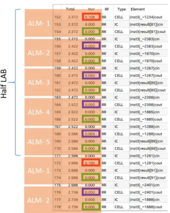
The logical structure of the Cyclone V is based on the logic array blocks (LABs). The LAB in Cyclone V is composed of ten adaptive logic modules (ALMs) that could be configured to perform logic, arithmetic and register functions. As presented in Fig. 2, each ALM contains four 4-input look-up tables (LUTs), two dedicated adders and four registers. The output of each adder could be sampled by two registers while the carry connections between the dedicated adders provide a fast carry chain along the LABs existing on the same column [9]. The studied TDL-based TDC makes use of the carry chain to enhance the resolution. The elementary cell of the delay line is the adder. That could be achieved by developing an M-bit adder VHDL code, proposed in [5], where M is the number of the delay cells. The latter is determined by the system clock period and the delay of the one-bit adder. The sum-out outputs of the cascaded adders consisting the delay line are sampled by the registers line (RL) at the rising edge of the system clock.
Two practical issues must be considered. Firstly, since the two operands of each adder are constants ‘1’ and ‘0’, the Quartus software would simplify the design and the delay line would not be placed when the design is compiled. To prevent that, the TDL block should be set as a design partition. Secondly, Quartus might place some adders and their corresponding registers in different ALMs, which causes a large variation in the delays from the sum-out of the adders to the data input of the corresponding flip-flops and the effect of the clock skew will be aggravated. To avoid this misplacing, both the adder block and the register block should be instantiated in an upper-level block and a logic lock region should be created for this block using the chip planner tool. The width of this region should be 1 and its height (the number of LABs consisting this region) should be calculated according to the required number of the delay elements M. Since there are 20 adders in each LAB, the region’s height equals to M divided by 20. Another interest of creating a logic lock region for the TDL is to control its physical placement by specifying its origin. The effect of the physical placement on
Fig. 2. ALM in arithmetic mode for Cyclone V devices [9]
the TDC performance could be experimentally observed in order to choose the origin that provides the best performance.
B. Carry chain timing analyzing in Cyclone V FPGA
The timing analysis results of the carry chain path, obtained by using the Timing Analyzer tool, indicate that the propagation delay is not identical for all the adders. Furthermore, the following points were observed:
Firstly, the path report of a 1024-cell TDL shows that the propagation time from the first adder to the last one is 31.57 ns, whereas the experimental results indicates that the true propagation time is 6.4 ns. Experimental tests were performed on TDLs with different number of cells show that the timing results obtained by the Timing Analyzer should be divided by 5 to give the approximate true timing values. This fact goes along with the results provided by [8]; stating that the propagation time of 691 adders is about 4 ns. This discrepancy between the experimental and the timing analyzer results is probably due to the timing analyzer model that failed to asses a good timing with such an optimized routing topology (with very short propagation delays of some ps). Indeed, the logic cell in a standard compilation are generally spread along the LAB resulting in a longer mean delay.
The second point is that the propagation delay is not identical for all the adders but differs according to the order of the adder in the ALM and the position of the ALM in the LAB. The timing analyzing results presented in Fig. 3 show that: • The first adder existing in the first and the sixth ALM of a
LAB has an approximate propagation delay of 100 ps. Dividing this value by 5 gives a real propagation delay of 20 ps for these two adders.
• For the other ALMs, the first adder has an approximate propagation delay of 50 ps. Therefore, the real delay (extracted from experiments) of these adders is 10 ps. • The propagation delay of the second adder in all the ALMs
is 0 ps.
• The delay from the sum-out of the first adder in an ALM to the data input of its corresponding flip-flop is 425 ps (real value is 5 times lower i.e. 85 ps), whereas for the second adder, this delay is 154 ps (real value is 30.8 ps). These differences in the propagation time of the adders as well as from the adders to their corresponding flip-flops, in addition to the clock skew, cause grate differences in the bins’ widths, which leads to a nonlinear TDL. Furthermore, the TDL will have many zero-width bins and large bubbles will appear in the thermometer code at the output of the TDL.
Fig. 3. Timing Analyzer: Carry chain path report .
Nevertheless, the propagation time differences could be useful to improve the TDL resolution but complicated bin realignment operations should be applied to overcome the bubble effect [8].
C. TDC implementation
A temporal resolution of 20 ps is generally sufficient for most TCSPC based applications that involve a Single Photon Avalanche Diode (SPAD) device as a light detector since the jitter of the SPADs is of some tens of picoseconds [10]. Hence, in order to reduce the nonlinearity and the bubble effect, and according to the timing characteristics stated above, the TDL could be designed by combining several adders in one TDL cell in a way that all the cells has the same targeted propagation times of almost 20 ps. As illustrated in Fig. 4, the following approach fulfills that:
• Each LAB is composed of an upper half and a lower half. These two halves are identical in terms of propagation time properties; each half consists of five ALMs, and the propagation time of the ALM, comprising two adders, is (20 + 0 = 20 ps) for the first ALM and (10 + 0 =10 ps) for the next four ones.
• Three TDL cells with identical propagation time of (20 ps) could be implemented in each half LAB. The first cell is composed of the two adders of the first ALM. The second one is composed of the four adders existing in the second and the third ALMs. The third cell is composed of the four adders of the fourth and the fifth ALMs. This approach is applied for all the half LABs consisting the TDL. Fig. 5 presents the behavioral VHDL code developed to link the adders’ line to the registers line for a 256-cell TDL TDC in order to apply this approach.
It is important to note that due to the high speed of the carry chain in the Cyclone V FPGA family, a very high frequency is required to clock a short TDL line if the cell is composed of only one adder (667 MHz for 256-cell TDL).
Fig. 4. Chip planner: Delay cells and registers in a logic array block.
Fig. 5. Linking adders to registers line VHDL model.
Otherwise, for a reasonable frequency, a large number of one-adder cells is required to cover all the clock period (855 cells for 200 MHz) which increases the encoding time and thus the TDC’s dead time. Hence, our design provides a good compromise (256 cells for 200 MHz) since the resolution is not the most critical factor for the intended application.
IV. DESIGN METHODOLOGY
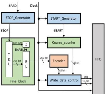
A. Global system structure
Fig. 6 demonstrates the global structure of the studied TDC system. In this system, as most of the TCSPC-based systems, the light emission is piloted by a synchronous signal, called the START signal, generated by the system (the START_Generator block). Therefore, TFine1, mentioned in the
timing diagram illustrated in Fig. 1, is equal to 0 and the TDC is reduced to a coarse block and one fine block [5], and the equation (1) is simplified to:
Fig. 6. Design’s global structure .
The START signal, which is a clock-width pulse, clears the COARSE counter. After that, this counter starts incrementing at the system clock. When a photon is detected by the SPAD, the STOP-Generator block sets the STOP signal to ‘1’. At the rising edge of this signal, the value of the COARSE counter is latched giving the coarse interval (Tcoarse).
The STOP signal also propagates through the TDL generating a thermometric code. This code is sampled by the registers line at the first clock rising edge to be encoded by the encoder block to a binary value (Tfine2). The WRITE_Data_Control
block is a finite-state machine that controls the coarse-fine data writing to a (FIFO) memory. When a photon is detected and the STOP signal is high, this state machine waits for a certain number of clock periods before writing the data to the FIFO in order to give the encoder the required time to finish the encoding process. After writing the data, this block sends a clock-width pulse to the STOP_Generator to reset the STOP signal to ‘0’.
B. Timing considerations
In such systems, the routing topology has an important effect on the system behavior. As mentioned before, the TDL output should be sampled by the RL at the first clock rising edge that follows the STOP signal edge. In order to achieve that, the STOP signal is sampled at the clock rising edge by a flip-flop, and the output signal of this flip-flop is inverted and used to enable the RL flip-flops. Thus, the ENABLE signal is set to ‘0’ after the first clock edge and disables the RL. The ENABLE signal should arrive to the RL during the clock period after the arrival of the STOP signal to the TDL. If the ENABLE signal arrives before the STOP signal, the TDL output will be sampled at the clock edge that comes before the propagation of the STOP signal resulting the code 255 at the TDL output and the bin 255 will have a large width. If the ENABLE signal is delayed more than a clock period, the TDL output will be sampled at the second following clock edge after the STOP signal. i.e. the STOP signal propagates all through the TDL resulting the code 0 at the TDL output and the bin number 0 will have a large width. In fact, mastering the arrival timing of the ENABLE signal is the most critical issue in our design. It was experimentally noticed that the ENABLE signal, with no constraints taken, arrives before the STOP signal. Furthermore, its arrival timing differs with every
new compilation or when the TDL placement is changed. Therefore, to overcome this issue, the ENABLE signal is generated by sampling the STOP signal just before the first TDL cell. To achieve that, the flip-flop that generates the ENABLE signal is placed at the beginning of the RL and sample the sum-out of the first adder, which is reset to ‘0’ once the STOP signal edge arrives. In this case, there will be no delay between the two signals. The timing analyzer results show that the ENABLE signal arrives to all the RL flip-flops in less than one clock period. Furthermore, this approach guarantees the same behavior when the design is recompiled. Nevertheless, it is recommended to perform an incremental compilation.
V. CONCLUSION
In this work, we have presented a design methodology for implementing a TDL TDC on Cyclone V FPGA targets. We have covered the ALM structures of this FPGA family and proposed an approach to overcome the delay differences along the carry chain, taking in consideration the different routing constraints that should be applied to force the desired placement of the TDL. We have also provided a simple approach that ensures the same functionality when the design is recompiled. The studied design was implemented and tested using a Cyclone V FPGA target, the achieved resolution is 19 ps which is sufficient for many TOF-based applications.
ACKNOWLEDGMENT
The authors would like to thank the French National Research Agency (ANR-15-CE11-0006) and the European Interreg WPS Project for funding this study.
REFERENCES
[1] T. Sui et al., "A 2.3-ps RMS resolution time-to-digital converter implemented in a low-cost Cyclone V FPGA," in IEEE Transactions on Instrumentation and Measurement, vol. 68, no. 10, pp. 3647-3660, Oct. 2019.
[2] Y. Wang and C. Liu, “A 3.9 ps time-interval RMS precision time-to-digital converter using a dual-sampling method in an ultrascale FPGA,” IEEE Trans. Nucl. Sci., vol. 63, no. 5, pp. 2617–2621, Oct. 2016. [3] Y. Wang and C. Liu, “A 4.2 ps time-interval RMS resolution
time-to-digital converter using a bin decimation method in an ultrascale FPGA,” IEEE Trans. Nucl. Sci., vol. 63, no. 5, pp. 2632–2638, Oct. 2016.
[4] R. Machado, J. Cabral and F. S. Alves, "Recent developments and challenges in FPGA-based time-to-digital converters," in IEEE Transactions on Instrumentation and Measurement, vol. 68, no. 11, pp. 4205-4221, Nov. 2019.
[5] F. Dadouche, T. Turko, W. Uhring, I. Malass, J. Bartringer, and J. Le Normand, “Design methodology of TDC on low cost FPGA targets,” in Proc. 9th Int. SENSORCOMM, 2015, pp. 29–34.
[6] J. Wu, Z. Shi, and I. Y. Wang, “Firmware-only implementation of time-todigital converter (TDC) in field-programmable gate array (FPGA),” in Proceedings of IEEE Nuclear Science Symposium Conference Record (IEEE, 2003), Vol. 1, pp. 177–181.
[7] F. Dadouche, et al., “Design implementation and characterization of time-to-digital converter on low-cost FPGA”, Sensors and Applications in Measuring and Automation Control Systems (Book Series: Advances in Sensors: Reviews), Chapter. 11, pp 205-229, Vol. 4, 2016. ISBN: 978-84-617-7596-5.
[8] H. Xia, G. Cao and N. Dong, “A 6.6 ps RMS resolution time-to-digital converter using interleaved sampling method in a 28 nm FPGA”. Rev. Sci. Instrum. 90, 044706, Apr. 2019.
[9] Intel Corporation, Cyclone V device handbook. volume 1, chapter 1, Oct. 2019.
[10] F. Ceccarelli, G. Acconcia, A. Gulinatti, M. Ghioni and I. Rech, "83-ps timing jitter with a Red-Enhanced SPAD and a fully integrated front end circuit," in IEEE Photonics Technology Letters, vol. 30, no. 19, pp. 1727-1730, 1 Oct. 2018.
![Fig. 2. ALM in arithmetic mode for Cyclone V devices [9]](https://thumb-eu.123doks.com/thumbv2/123doknet/14365313.503411/3.892.487.814.78.304/fig-alm-arithmetic-mode-cyclone-v-devices.webp)