HAL Id: hal-02505854
https://hal.archives-ouvertes.fr/hal-02505854
Submitted on 11 Mar 2020
HAL is a multi-disciplinary open access
archive for the deposit and dissemination of
sci-entific research documents, whether they are
pub-lished or not. The documents may come from
teaching and research institutions in France or
abroad, or from public or private research centers.
L’archive ouverte pluridisciplinaire HAL, est
destinée au dépôt et à la diffusion de documents
scientifiques de niveau recherche, publiés ou non,
émanant des établissements d’enseignement et de
recherche français ou étrangers, des laboratoires
publics ou privés.
Couplings between a resonant current source power
supply and a DBD excilamp
Hubert Piquet, D Florez, X. Bonnin, Antoine Belinger, R Diez
To cite this version:
Hubert Piquet, D Florez, X. Bonnin, Antoine Belinger, R Diez. Couplings between a resonant current
source power supply and a DBD excilamp. Atmospheric and oceanic optics, V.E. Zuev Institute of
Atmospheric Optics, 2014. �hal-02505854�
«Îïòèêà àòìîñôåðû è îêåàíà», 27, ¹ 4 (2014)
354 Piquet H., Florez D., Bonnin X. et al., 2014
Couplings between a resonant current source power supply
and a DBD excilamp
H. Piquet
1, D. Florez
2, X. Bonnin
1, A. Belinger
3, R. Diez
2*
1Institution Toulouse University. Institut National Polytechnique de Toulouse
2 rue Camichel-31071 Toulouse cedex, France
2Pontificia Universidad Javeriana
Carrera 7, N 40–62 Faculdad de Ingenieria-110231 Bogotá, Colombia
3Toulouse University. Université Paul Sabatier
118, route de Narbonne-31062 Toulouse cedex 9, France Ïîñòóïèëà â ðåäàêöèþ 6.03.2014 ã.
This paper presents a study of couplings which take place in systems where dielectric barrier discharge (DBD) excimer lamps are supplied with current source electrical power generators. Causal analysis, using the fundamental properties of the DBD, is used for the design of such current sources. A two steps approach is de-velopedhere:inorderto control the lamp power, with the best efficiency concerning the UV emission, a current shape controlled current generator is set-up to investigate the possible degrees of freedom of the current wave-forms: frequency, peak current, pulse duration.
Onthisbasis,“optimized”supplyingconditionsareselected,andasecondpowergeneratorwith high electri-calefficiencyisdesigned: its operating mode combines discontinuous current mode and soft-commutation (ZCS), obtaining as well low electromagnetic emissions and reduced switching losses. A classical electrical equivalent model of the lamp is used to achieve the state plane analysis and to calculate all the electric variables involved in the design of the converter and consequently to select its components. The mathematical relationships ob-tained from this process, especially those concerning the control of the injected power by means of the available degrees of freedom, are validated with simulations and experimental results. Experimental UV emission per-formances are presented as well.
Keywords: dielectric barrier discharge, excimer lamps, power supply, optimization, resonant inverter, UV.
Introduction
Excimer lamps are powerful and flexible emitters of narrow band UV radiations [1, 2], which applica-tions are currently more and more spreading out [3]. In the current context of transition from fundamental studies to industrial applications, the efficiency and controllability of the UV emission is of more and more important concern. In this aim, the study which is presented in this paper is focused on the definition of the most fitted characteristics of the electrical power generator associated to the lamp.
The choice of the characteristics of the power sup-plies for dielectric barrier discharge devices, and es-pecially for DBD excilamps, has been shown in a num-ber of previous papers to be of crucial importance for the overall system’s performances.
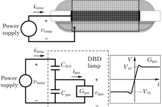
For instance, on the basis of the classical equiva-lent circuit of DBD devices [4, 5], which is reminded in Fig. 1, the comparison of the electrical simulation waveforms, obtained with pulsed voltage of pulsed current generators (square shapes) is exhibited in Fig. 2.
_____________
* Hubert Piquet ([email protected]); David Florez ([email protected]); Xavier Bonnin ([email protected]); Antoine Belinger ([email protected]);Rafael Diez (rdiez@ javeriana.edu.co).
Fig. 1. DBD excilamp. Structure and electrical model For these numerical simulations, the parameters of the equivalent circuit are adjusted to reflect the operation of a 100 W bulb filled with a Xe–Cl2 mix-ture (wavelength is 308 nm). The following values from Table 1 are taken into account; concerning the conductance of the gas in ON state, the voltage pla-teau across the latter is assumed to remain at the same Vth level as at the threshold time.
Although pulsed voltage sources have shown to be a performing solution at the experimental investi- gation’s step, a more reliable design and a tighter control of the performances are needed for industrial
Couplings between a resonant current source power supply and a DBD excilamp 355 a
b
Fig. 2. Voltage-mode converter with square voltage output and uncontrolled current (a), and current-mode converter
with square current and controlled voltage (b) – theoretical
simulation waveforms
T a b l e 1
Equivalent electrical parameters of a Xe–Cl2 DBD excilamp
Symbol Parameter Value
Vth Threshold voltage – plateau level 1310 V
Cdiel Dielectric barriers capacitance 85 pF
Cgas Gas gap capacitance 28 pF
Plamp Nominal lamp power 100 W
applications [2, 6, 7]. Indeed, the actual control of the power injected into the lamp by such a pulsed voltage generator is really difficult to predict: accounting the capacitive behavior of the DBD system, the magnitude and the duration of the obtained current spikes is re-lated to the slope and the duration of the voltage fronts [8, 9]. The latters are defined by the switching per-formances of the semiconductors used to produce the pulsed voltage and are really difficult to control in the supplying circuit, from the very first design step. On the contrary, as illustrated in Fig. 2, b, when the current injected into the DBD device is con-trolled [8, 10], the integral form of the capacitive behavior of the dielectric barriers can be used to de-fine and to predict, from the first design step, the shape and the magnitude of the voltage across both the lamp and the power generator, as well as all the other dimensioning electrical quantities.
1. Current source supply
for DBD lamps
In this section, we consider different issues, which are to be accounted when a current source generator is selected to supply a DBD device.
1.1. DBD lamp current shape properties
Taking into account the capacitive behavior of the DBD, whose equivalent circuit (Fig. 1) includes a Cdiel series capacitor, it is obvious that the average value of the current injected into the lamp, ilamp, needs to be null. If this condition is not fulfilled, the integral term of equation (1), which defines the voltage across the lamp, will take uncontrolled diverging values
gas
lamp lamp diel 1 . v v i dt C (1)In this scope, a full bridge topology (Fig. 3) is a good candidate to interconnect a current source J and the DBD device.
Fig. 3. Bridge configuration, associated with a generic cur-rentsource to supply a DBD excimer lamp (theoretical step)
Whatever the shape of the J current waveform, it offers, according to the different paths which are shown in Fig. 3, three possible values for the ilamp current: 1) +J (when power switches K1 and K2 are in ON state),
2) 0 (if one of the pairs {K1, K1} or {K2, K2} is ON),
3) –J (when K1 and K2 are ON).
On this basis, the fulfillment of the previous re-quirement is relatively simple and is mainly a matter of managing the durations of these three sequences.
1.2. Power switches properties
Assuming that the J current source is constant and that only +J and –J levels of the ilamp current are used, the following simulatet waveforms (Fig. 4) are presenting the operation of power switches K1 and K2. Similar results are obtained for power switches K4 and K3.
These waveforms are highlighting the need of thyristor-like devices [11], according to the following elements of the simulated behavior, as summarized in Fig. 5:
1) bidirectional voltage (OFF state), 2) controlled turn-on under positive voltage, 3) positive current conductive sequence (ON state), 4) spontaneous turn-off, leading to negative voltage. 11.*
356 Piquet H., Florez D., Bonnin X. et al.
a
b
Fig. 4. Simulated waveforms of voltage (a) and current (b)
of both K1 (black) and K2 (grey) power switches
Fig. 5. OperatingcharacteristicsofK1andK2powerswitches Taking also into account that the operating fre-quencies will be in the 10–200 kHz range, actual thyristor devices are not fitted and synthesized solu-tions need to be set up, with a mosfet-diode series association.
1.3. High voltage step-up transformer
Considering the voltage levels which are pre-sented on the waveforms of Fig. 4, usual MOSFETs and diodes are not adapted. For this reason, a step-up 1:n transformer needs to be introduced in the sys-tem. This device is inserted between the DBD lamp and the full bridge converter (Fig. 6); it reduces in an n ratio the voltages which are seen across the ter-minals of the bridge devices.
Fig. 6. Thyristor-likedevicesfullbridge configuration, con-nected to the DBD excimer lamp, through a step-up high voltage transformer
According to the voltage levels which are expected across the lamp (i.e., 4–5 kV), a ratio value 1:10 to 1:12 is selected.
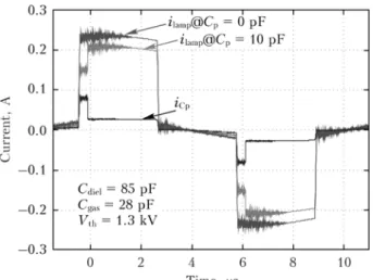
Effect of the parasitic capacitance of the HV transformer
Since the DBD lamp is an electrical load of ca-pacitive nature and its capacitances are in the order of pF (see Table 1), the design of the transformer is a key aspect for the good performance of the power supply. As a matter of fact, the inter-winding capaci-tances of the transformer strongly decrease the power injected in the DBD [10]. Assuming that the trans-former is highly coupled, that the study focuses only on low frequency phenomena (e.g., which do not involve the leakage inductance), and that the inter-winding voltage Vps is well defined, the high voltage trans-former can be modeled by the scheme presented in Fig. 7, where Vps is assumed to be proportional to the secondary potential V2 in order to take into ac-count several connection schemes.
Fig. 7. Low frequency equivalent circuit (primary voltage is neglected, when compared to the secondary one) of the high voltage transformer
If Cp is comparable to the lamp equivalent ca-pacitance, a current divider effect takes place and a considerable amount of the supply output current is derived through Cp, penalizing the efficiency or even forbidding the lamp ignition.
Fig. 8 presents the current of the lamp for two different value of the Cp capacitance (simulation re-sults). One can notice the distortion of the expected square shape current injected into the DBD lamp. The latter takes place at the moment of the change of the direction of the current (by mean of the inverter presented in P. 1.1).
Couplings between a resonant current source power supply and a DBD excilamp 357 Fig. 8. Distortion of the square current injected into the
DBD lamp, due to the Cp parasitic capacitance of the high
voltage transformer
This phenomenon provokes a delay of the associa- ted ignition of the plasma (indeed, the gas voltage needs to change from +Vth to –Vth, or, vice versa, as a result of the charge transfer which takes place in the Cgas capacitance).
Elements for the design of the HV transformer On the basis of analytical calculations, the elec-trostatic energy W which is stored in the volume of the transformer is calculated [12]. This calculation takes into account the geometrical and physical parameters of the transformer, but also the way the secondary potential is related to the primary one through Vps. According to Fig. 7, the electrostatic energy stored into the transformer W, can be expressed by:
2 p 2 1 , 2 W C V (2)
where Cp explicitly depends on k and on the trans-former building parameters (the way the turns are arranged, the number of layers, the insulation layers materials and thicknesses, etc.). Given the small value of the lamp equivalent capacitance (see Table 1), a low transformer’s output capacitance Cp is mandatory; in order to minimize Cp, several winding configurations have to be considered. The secondary winding can be split in several sections (Fig. 9).
Fig. 9. Organizationofthewindings of the high-voltage step uptransformer:high voltage winding is organized in sections (here, 2 sections). Each section gathers turn layers separated by insulating tapes
On the basis of analytical calculations, using the geometrical properties of the arrangements of the windings (Fig. 9), the electrostatic energy W which is stored in the volume of the transformer (i.e., volume of the windings layers, insulations layers, free space between the windings and the core) is calculated [12]. This calculation takes into account the Vps potential of the secondary winding with respect to the primary one, thus accounting for grounding properties.
Being an analytical expression which incorpo-rates the winding organization and the transformer’s geometrical parameters, Cp is used to implement an optimizing algorithm which helps in designing the windings to minimize the parasitic effects.
The step-up ratio being chosen, for a fixed mag-netic core, a fixed number of turns, a fixed number of layers, and a fixed amount of insulation material, the theoretical study of [12] shows that splitting the secondary winding allows reducing the value of Cp and that there is an optimal way to define the secon-dary winding potential through the value of k.
In Fig. 10, the “W versusk” curves of a particular four-layers high voltage step-up transformer are com-pared for several numbers of sections (which are con-nected in series).
Fig. 10.Optimizationofthewinding’s arrangement (N1 = 4)
The value of Cp can be reduced by a factor 3 by splitting the secondary winding in four sections and a lower Cp value can be reached by wisely choos-ing the value of k.
2. Square shape current source supply
In this section, we outline the main properties of a square shape current converter for the supply of DBD lamps; then, we consider the use of the 3 de-grees of freedom (DOF) offered by this generator to define the best operating conditions, focusing on the UV emission performances.
2.1. DC current source design
The proposed topology is a cascade association (Fig. 11) of:
– a two quadrants chopper (2-Q Chopper) aimed at producing a constant J current; the design of the latter is detailed in [10, 13];
358 Piquet H., Florez D., Bonnin X. et al.
– a full bridge which has been introduced in Fig. 3, and permits to inject a three level current (–J, 0, +J) into the bulb (see Fig. 12). The latter is designed according to the directions given in P. 1.2;
– a step-up high voltage transformer.
Fig. 11. Cascade topology of the square shape current
generator
Fig. 12. Theoretical output current of the square shape
generator
Accounting a 6 kV maximum voltage across the terminals of the lamp, and using 1 kV rated semi-conductors (used with a 40% safety margin) for the full bridge, the step-up ratio of the transformer takes a 1:10 value. Its operating frequency is defined by the inverter; being dedicated to investigations and seeking the optimal conditions, a 50–200 kHz fre-quency range has been considered. Litz wires are used for the primary wing and mono-strand wires are used for the secondary. The gauge is selected according to the transferred power (100 W).
As developed in [14], Vth being the voltage across the gas when the discharge is alight, J, the magni-tude of the current delivered by the current source (2-Q Chopper), and flamp and Dlamp, the frequency and the duty ratio of the ilamp waveform controlled by the bridge, it can be established that the electrical power injected into the bulb is:
2 th th gas
lamp lampV – 4lamp V .
P JD f C
n n (3)
For a given power level, any combination of these three degrees of freedom (DOF: J, flamp, and Dlamp)
does not produce the same UV emission. Parametric investigations related to the UV emission are develo- ped in the next section.
2.2. Using the DOF of the square shape
current source to experimentally optimize
the UV emission
Experimental setup
It has been observed that the UV emission level is sensitive to the operating temperature of the bulb. For this reason, considering here steady state perform-ances, a cooling apparatus has been built, with fans organizing air circulation outside as well as through the inner pipe of the bulb. Additionally, temperature monitoring has been used and measurements of the UV emission are realized when stable temperature is observed. The UV instantaneous waveforms of this lamp (wavelength 308 nm) are captured using a THORLABS PDA-25K photo-detector, and the UV power is measured with a GIGAHERTZ-OPTIKP9710 photometer using a UV detector SN5816, configured with an integration time of 0.5 s and a dose time of 5 s, installed at 3 mm of the lamp surface.
Experimental waveforms of Fig. 13 illustrate the operation of the square shape current source generator. The primary current (iprim) appears to be well con-trolled, as theoretically expected in Fig. 12.
Fig. 13. Experimentalperformancesofthe square shape cur-rent source at 60 kHz: primary curcur-rent iprim (1 A/div), lamp
current ilamp (200 mA/div), and voltage Vlamp (2 kV/div),
UV emission (a.u.); horizontal: 5 s/div
The lamp current (ilamp), although similar, suffers of relatively limited effects of the parasitic elements of the high voltage transformer. As already stated in [9], the instantaneous UV appears to be tightly correlated with the current waveform. According to equation (1), the lamp voltage (Vlamp) presents the expected shape.
Effect of the operating frequency
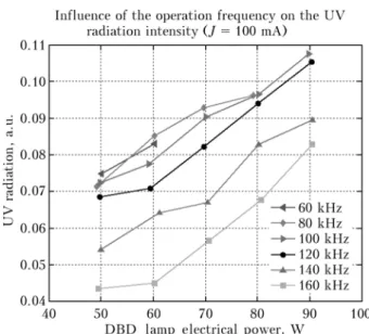
The first measurement set (Fig. 14) explores the effect of the operating frequency on the lamp effi-ciency: for a given current magnitude (here 100 mA), the electrical power injected into the bulb is changed, for different frequencies, using the Dlamp duty ratio DOF. UV power is measured at each point.
Couplings between a resonant current source power supply and a DBD excilamp 359 Fig. 14. XeCllampUVradiation power (mW/cm2) vs.
elec-trical power injected in the DBD. Each line corresponds to a different frequency. The power is adjusted by means of the duty ratio Dlamp
Curves of Fig. 14 show that the most performing conversion from electrical power to UV power is achieved in this bulb with frequencies between 60 and 80 kHz. With higher frequencies, the efficiency appears to decrease.
Effects of the current shape parameters For a given frequency, the shape of the current injected into the lamp can be tuned by mean of two DOFs: the current magnitude J and the duty cycle, Dlamp (together with the operating period 1/flamp, the latter defines the duration of the current pulses: Dlamp/flamp). Fig. 15 presents, for the best fitted fre-quency selected at the previous step (70 kHz), the UV dose obtained (over a 30 s time interval integra-tion) with various (J, Dlamp) combinations.
Fig. 15. UVdoseatflamp = 70 kHz,Plamp = 79.9 W, vs.
cur-rent magnitude J (the duration of the pulses is adjusted
to maintain the chosen Plamp power value)
It appears from the trend shown in Fig. 15 that the highest the magnitude of the current pulses (and thus the shortest the duration of the current pulse),
the most efficient will be the conversion from electri-cal power to UV; the difference can reach a 40% level. Nevertheless, the actual control of these current pulses is limited by two factors. The current sizing of the semiconductor devices limits the J value. And their switching speed, as well as the leakage induc-tance of the transformer, which causes an overlapping phenomenon in the bridge’s switching, do not allow duration shorter than a given amount (and thus lim-its the lowest value of the Dlamp parameter).
Discussion concerning the current square shape generator
From the previous parts, it clearly appears that this generator is a very flexible and valuable investi-gation tool, in order to determine, thanks to its three available DOFs, the most desirable supplying condi-tions for the DBD excilamps.
Nevertheless, its operating performances do not allow imagining using such a topology for actually supplying a DBD excilamp integrated within an indus-trial process. Indeed, mainly because of the switching losses in the semiconductor devices (which are opera- ting in hard switching conditions), the global electri-cal efficiency of this generator hardly overcomes the 50% level; for a given operating point, the measure-ments and the conditions are summarized in Table 2.
T a b l e 2
Main parameters, losses, and efficiency of the square shape current generator
Symbol Parameter Value
Vin DC voltage level 300 V
flamp Frequency of the current inverter 50 kHz
Plamp Lamp electrical power (measure) 56.6 W
Pin Power taken from the DC source 99.6 W
CVS Efficiency of the generator 57%
transfo Efficiency of the sole transformer 88%
For this reason, a more performing topology is considered in the next part. The design of this new converter is especially oriented towards the optimal conditions obtained thanks to this parametric study: with the bulb used for our experimentations, we ob-tained finally the conditions which offer the best overall efficiency, summarized in Table 3.
T a b l e 3
DBD lamp optimal supply conditions – values of the DOFs
Symbol Parameter Value
J Lamp current magnitude 250 mA
flamp Frequency of the lamp current 80 kHz
Dlamp Duty ratio of the lamp current 25%
360 Piquet H., Florez D., Bonnin X. et al.
3. Resonant Current source supply
for DBD lamps: series inverter
in discontinuous mode
3.1. Operating principle and design
According to the specifications summarized in Tab- le 3, a series resonant inverter (SRI) operating in dis-continuous mode (DCM) has been studied [5, 14, 15]. In Fig. 16, one can recognize the bridge topology, which is used to invert the lamp current. The current source associated with the latter is built by mean of a DC voltage source Vin, in series with a L inductor.
Fig. 16. Circuit of series resonant inverter in discontinuous
mode
Resonant topologies have already been proposed in the literature [6, 16, 17] for lamps and DBDs con-trol purposes. The SRI’s operating principle is now analyzed; it is summarized on the waveforms of Fig. 17 and on the set of equivalent circuits presented in Fig. 18.
Fig. 17. Waveforms of series resonant inverter in disconti-
nuous mode
Starting with null current in L inductor and nega-tively charged dielectric barriers of the bulb, switches K1 and K4 are turned ON.
This causes a positive half oscillating period in the resonant circuit built up with L and the capaci-tances of the lamp: Ceq (which includes the gas and the dielectric capacitance), the equivalent capacitance of the lamp when the gas is not alight (seq. a) or Cgas when the latter is ON (seq. b). This oscillation finishes when the current returns to 0 and switches K1 and K4 naturally (being unidirectional in current) turn OFF. The lamp voltage has been inverted du- ring this half period.
a b c
d e f
Fig. 18. Operationofseriesresonantinverterindiscontinuous
mode
All the switches remain OFF during a chosen time interval (seq. c), which depends on the value of the operating frequency; and the lamp voltage re-mains unchanged (positive voltage).
When switches K2 and K4 are turned ON, a sym-metrical set of sequences (d, e, f) starts and produces a negative current pulse in the lamp; at the end of the latter, the lamp voltage has returned to its negative va- lue, which is its periodic steady-state initial condition. The characteristics of the current pulses (magni-tude and duration depend on the value of the L in-ductor as well as on the equivalent circuit’s parame-ters of the lamp: Cdiel, Cgas, and Vth. Following equa-tions (4) and (5) define the peak value of the lamp’s electrical quantities; they are needed to achieve the design of the supply:
2 gas in lamp th th diel th ˆ ( – ) ; V V V C C V nV (4) 2 in lamp lamp diel
ˆ (ˆ ) ( ).
I V nV C n L (5)
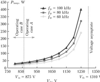
Note: in equation (5), “–” has to be considered if the gas turns ON before the peak value of ilamp, case A, right part of curves in Fig. 19, which is shown on the waveforms of Fig. 18; otherwise “+” has to be used, case B, left part in Fig. 19.
Fig. 19. Power delivered into the lamp by SRI generator:
Plamp vs. nVin (n = 10) for different frequencies (60, 80,
Couplings between a resonant current source power supply and a DBD excilamp 361
3.2. Couplings between the supply
and the DBD lamp
Analytical calculations lead to equation (6), which gives the power injected into the lamp
2 th gas lamp lamp th in th 4 – 1 . – V P f V C V nV (6)
According to this equation, a stability criterion of the whole system (SRI generator + lamp) is given by relation (7):
in th.
nV V (7)
This condition appears in the characteristics set plotted in Fig. 19. The latter shows that, according to equation (6), two degrees of freedom, flamp and Vin, are available to control the power injected into the lamp. One should also notice that formula (6) of Plamp highlights the couplings of the supply and the bulb: indeed, Plamp depends not only on the operating con-ditions defined by the inverter (flamp and Vin), but also on the lamp parameters (Cgas and Vth).
3.3. Experimentations and performances
An experimental setup of the SRI inverter has been designed and realized to supply the previously described Xe–Cl2 excilamp, which parameters are given in Table 1. This power supply presents the fol-lowing characteristics (Table 4).
T a b l e 4
SRI experimental setup: main characteristics
Symbol Parameter Value ˆIlamp Lamp current peak value 150 mA
flamp Frequency of the lamp current 80 kHz
Duration of the current pulses s
Plamp Lamp electrical power 75 W
As shown in Fig. 20, experimental measurements (a) are in very good agreement with the simulated wave-forms (b) used for the design of the SRI inverter.
Furthermore, excellent electrical performances are achieved thanks to the proposed topology (an opti-mized transformer has been used for this prototype) (Table 5).
T a b l e 5
Efficiency of SRI current generator
Symbol Parameter Value, %
bridge Efficiency of H bridge + inductor 96
transfo Efficiency of the transformer 95
CVS Efficiency of the SRI generator 91
Additionally, very low level EMC perturbations are produced, thanks to the smooth waveforms (com-pared to the ones of the square shape current source). Concerning the UV emission, the photo-detector measurements presented in Fig. 21 highlight the tight
a
b
Fig. 20. Converter and DBD lamp waveforms from simula- tion (a) and from the experimental validation (b)
correlation between the lamp current (hence the gas conduction’s current [8, 9]) and the UV emission. This property has already been shown with the square shape current source (see Fig. 13).
Fig. 21. Experimental measurements: electrical quantities and UV emission; horizontal: 5 s/div
According to the experimental characteristic of Fig. 14, the adjustment of the electrical power by means of the Vin voltage allows to control the UV power with the best lamp efficiency (flamp being tuned to the optimal 80 kHz value).
362 Piquet H., Florez D., Bonnin X. et al.
Conclusion
For the supply of DBD UV lamps, a systemic study is carried out, in the framework of which two current controlled generators are studied and designed. The square shape one is a very valuable tool for in-vestigating the operating conditions of the lamp. It is used to define the optimal set of parameters (current pulse magnitude and duration, frequency). But its elec-trical performances (efficiency, perturbations, dimen-sioning of the components) are rather poor. The analy-sis of the performances of this generator also high-lights the key-role of the step up transformer in the control of the power transfers. On the basis of the parametric study, optimal supplying conditions of the selected Xe–Cl2 excimer lamp are defined and a series resonant current inverter, operated in discontinuous mode, is studied and designed to meet these specifica-tions with the best performances. Furthermore, it of-fers power adjustment capabilities, by means of two degrees of freedom (frequency and supplying voltage), which are combined with the parameters of the sup-plied bulb, highlighting the very tight couplings be-tween this generator and its load.
The authors are grateful to the French-Colombian cooperation (ECOS Nord, COLCIENCIAS-ICETEX program) and to the French Midi-Pyrenees region for support.
This paper has been written on the basis of a pre- sentation at AMPL’2013 conference (Atomic and Mole- cular Pulsed Lasers-2013), Tomsk, 16–20 of September. 1. Kogelschatz U. Dielectric-Barrier Discharges: Their
His-tory, Discharge Physics, and Industrial Applications // Plasma Chemistry and Plasma Processing. 2003. V. 23, N 1. P. 26–31.
2. Lomaev M.I.,Skakun V.S.,Sosnin A.,Tarasenko V.F., Shitts D.V., Erofeev M.V. Excilamps: efficient sources
of spontaneous UV and VUV radiation // Physics Us-pekhi. 2003. V. 46, N 2. P. 193–209.
3. Sosnin E.A.,Oppenländer T.,Tarasenko V.F.Applications ofcapacitiveandbarrierdischargeexcilampsinphotoscien- ce // J. Photochemistry and Photobiology C: Photo-chemistry Reviews. 2006. V. 7, N 4. P. 145–163. 4. Diez R., Salanne J.-P., Piquet H., Bhosle S., Zissis G.
Predictive model of a DBD lamp for power supply de-sign and method for the automatic identification of its parameters // The European Physical J. Phys. D: Appl. Phys. 2007. V. 37, N 3. P. 307–313.
5. Lopez A.M., Piquet H., Patino D., Diez R., Bonnin X.
ParametersIdentification and Gas Behavior Characteri- zationofDBDSystems//IEEETrans.on Plasma Scien- ce. 2013. V. 41, N 8. P. 2335–2342. DOI: 10.1109/ TPS.2013.2273462.
6. Mildren R., Carman R., Falconer I. Visible and VUV
emission from a xenon dielectric barrier discharge using pulsed and sinusoidal voltage excitation waveforms // IEEETrans.onPlasmaScience.2002.V. 30.P. 192–193.
7. Williamson J.M., Trump D.D., Bletzinger P., Gangu-
ly B.N. Comparison of high-voltage ac and pulsed ope-
ration of a surface dielectric barrier discharge // J. Phys. D: Appl. Phys. 2006. V. 39. P. 4400–4406. 8. Diez R., Piquet H., Cousineau M., Bhosle S.
Current-Mode Power Converter for Radiation Control in DBD Excimer Lamps // IEEE Trans. on Industrial Electro- nics. 2012. V. 59, N 4. P. 1912–1919.
9. Piquet H., Bhosle S., Diez R., Erofeev M. Pulsed
Cur-rent-Mode Supply of Dielectric Barrier Discharge Ex-cilamps for the Control of the Radiated Ultraviolet Power // IEEE Trans. on Plasma Science. 2010. V. 38, N 10. P. 2531–2538.
10. Bonnin X.,Piquet H.,Naudé N.,Bouzidi M.C.,Gherar- di N., Blaquière J.-M. Design of a current converter to
maximize the power into homogeneous dielectric barrier discharge (DBD) devices // The European Physical J. Appl. Phys. 2013. V. 64. P. 10901. DOI: 10.1051/ epjap/2013130080.
11. Cousineau M., Diez R., Piquet H., Durrieu O.
Synthe-sized High-Frequency Thyristor for Dielectric Barrier Discharge Excimer Lamps // IEEE Trans. on Industrial Electronics. 2012. V. 59, N 4. P. 1920–1928.
12. Bonnin X.,Piquet H., Diez R., Florez D. Designing the
high voltage transformer of power supplies for DBD: Windings arrangement to reduce the parasitic capacitive effects//15th EuropeanConference on Power Electro- nicsandApplications(EPE).2013.P. 1–9.DOI:10.1109/ EPE.2013.6631928
13. Flórez D., Diez R., Hay K., Piquet H. DBD Excimer
Lamp Power Supply with Fully Controlled Operating Conditions // OPTIM Conf., IEEE. 2012.
14. Flórez D. Power supplies for the study and efficient use
of DBD excimer lamps // PHD thesis from University of Toulouse (France). January, 2014.
15. Chéron Y.SoftCommutation.London:Chapman& Hall, 1992.
16. Kalisiak S.,Holub M., Jakubowski T. Resonant inverter
with output voltage pulse-phase-shift control for DBD plasmareactorsupply// 13th European Conf. on Power Electronics and Applications, EPE'09. 2009.
17. Alonso J., Garcia J., Calleja A., Ribas J., Cardesin J.
Analysis, design, and experimentation of a high-voltage power supply for ozone generation based on current-fed parallel-resonant push-pull inverter // IEEE Trans. on Industry Applications. 2005. V. 41, N 5. P. 1364–1372. 18. Meisser M., Kling R., Heering W. Universal Resonant
Topology for High Frequency Pulsed Operation of Di-electricBarrierDischargeLightSources//AppliedPo- wer ElectronicsConf.and Exposition(APEC). Twenty-Sixth Annual IEEE, 2011.
19. Flórez D., Diez R., Piquet H. Series-resonant inverter
in DCM mode for the supply of a DBD excimer UV lamp // Industry Applications Society Annual Meeting (IAS). IEEE. 2012. P. 1–8.


![Fig. 20. Converter and DBD lamp waveforms from simula- tion (a) and from the experimental validation (b) correlation between the lamp current (hence the gas conduction’s current [8, 9]) and the UV emission](https://thumb-eu.123doks.com/thumbv2/123doknet/14369111.504059/9.892.481.814.126.608/converter-waveforms-experimental-validation-correlation-current-conduction-emission.webp)
