Commercialization of Germanium Based
Nanocrystal Memoryby Kian Chiew Seow B.Eng., (Electrical Engineering) National University of Singapore, 2006
SUBMITTED TO THE DEPARTMENT OF MATERIALS SCIENCE AND ENGINEERING
IN PARTIAL FULFILLMENT OF THE REQUIREMENTS FOR THE DEGREE OF MASTER OF ENGINEERING IN MATERIALS SCIENCE AND ENGINEERING
AT THE
MASSACHUSETTS INSTITUTE OF TECHNOLOGY SEPTEMBER 2007
C 2007 Massachusetts Institute of Technology All rights reserved
Signature of
Author:... . ...
Department of Materials Science and Engineering July 23, 2007 Certified
by: ... I•.C ... l V.. Thompson Carl V. Thompson Stavros Salapatas Professor of Materials Science and Engineering Thesis Supervisor Accepted
by: ... . W .
Samuel M. Allen POSCO Professor of Physical Metallurgy Chair, Departmental Committee on Graduate Students
LIBRARIES
ARGES
MASSACHUsSTTS INSTITrUEOFTECHNOLOGY
SEPO
2
4
2007
Commercialization of Germanium Based Nanocrystal Memory
By
Kian Chiew Seow
Submitted to the Department of Material Science and Engineering On August 1, 2007 in Partial Fulfillment of the
Requirements of the Degree of Master of Engineering in Material Science and Engineering
ABSTRACT
This thesis explores the commercialization of germanium-based nanocrystal memories. Demand for smaller and faster electronics and embedded systems supports the development of high-density, low-power non-volatile electronic memory devices. Flash memory cells designed for ten years of data retention require the use of a thick tunneling oxide. This compromises writing and reading speed as well as endurance. A smaller device size can be achieved and speed and can be improved by decreasing the oxide thickness. However, significant charge leakage will occur if the oxide is too thin, which will reduce the data retention time dramatically. This imposes a limit to the amount by which the oxide thickness can be decreased in conventional devices. Research has shown that by incorporating nanocrystals in the tunnel oxide, charge traps are created which reduce charge leakage and improve endurance through charge-storage redundancy. By replacing the conventional floating gate memory with one using Si or Ge nanocrystals, the nonvolatile memory exhibits high programming speed with low programming voltage and superior retention time, and yet is compatible with conventional silicon technology. This thesis provides an analysis of competing technologies, an intellectual property analysis, costs modeling as well as ways to improve nanocrystal memories in order to compete with other forms of emerging technologies to replace conventional Flash memories.
Thesis Supervisor: Carl V. Thompson
Title: Stavros Salapatas Professor of Materials Science and Engineering
ACKNOWLEDGEMENTS
This thesis would not have materialized with the help, guidance and support of many people. First and foremost, I would like to thank Prof. Carl Thompson from the Massachusetts Institute of Technology (MIT) and Prof. Choi Wee Kiong from the National University of Singapore (NUS) for their guidance. I would also like to thank Prof Chim Wai Kim from NUS for lending me literature pertaining to nanocrystal
memories.
I would also like to thank Dr. Vincent Ho and Mr Chin Khee Yeap from the semiconductor industry for providing me with estimated figures for the costs models. The administrative officers from the Singapore-MIT alliance (SMA) office as well as the Department of Material Science and Engineering (DMSE) Office are also a great help. Special thanks to Ms Jocelyn Sales and Ms Juliana Chai for their assistance and help rendered throughout my entire course of studies.
In addition, I would also like to thank Roy, Zhengfei, Hongpeng and Zhihao from the Microelectronics Lab in the National University of Singapore for the time spent with me in discussing technical aspects pertaining to nanocrystal memories.
This thesis would also not be possible without the support of my fellow coursemates from the Singapore-MIT alliance program and the Massachusetts Institute of Technology, my housemates as well as my friends.
I would like to thank my family for having stood by me for all 26 years of my life. Last but not least, I would like to give my warmest thanks to professors in MIT and NUS who have taught me, and anyone who is not mentioned here but has helped me in one way or another.
Contents
1. Introduction1.1 History of Non-volatile Memory Structures 10 1.2 Working Principles of Conventional Flash Memory 13 1.3 Current and Future Non-volatile Memories 16
1.4 Nanocrystal Memory 22
Chapter 1 References 23
2. Nanocrystal Memory
2.1 Nanoceystal Memory Device 27
2.2 Synthesis of Germanium Nanocrystals 30
2.3 Characterization of Nanocrystals 33
2.4 Charge Storage in Nanocrystal Memory Devices 34
2.5 Optimum Nanocrystal Size 43
2.6 Comparison of Different Nanocrystal Memory 48
2.7 Hetero-nanocrystal Memory 50
2.8 Comparison between NC Memory and other 57 Flash Replacement Technologies
2.9 Multi-bit Schemes 62
3. Market and Intellectual Property Analysis
3.1 Market Overview 75
3.2 Market Growth 79
3.3 Competitors 83
3.4 Intellectual Property 84
3.5 Market and Intellectual Property Analysis Conclusion 86
Chapter 3 References 86
4. Cost Modeling
4.1 Chip Industry Trends 90
4.2 Cost Model of Building a Fabrication Plant 94
4.3 Cost Modeling Conclusions 96
Chapter 4 References 97
5. Conclusions
List of Figures
Figure 1.1: Schematic of a Floating Gate Device
Figure 1.2: (Top) NOR Flash Memory and Wiring on Silicon. (Bottom)) NAND Flash Memory and Wiring on Silicon.
Figure 1.3: (Left) Schematic Comparison between a Floating Gate Structure and a SONOS Structure (Right) A Transmission Electron Microscopy (TEM) Image of the SONOS Structure
Figure 1.4: Schematic of Phase Change Memory
Figure 1.5: A MRAM Cell During Read (Above) and Write (Below) Operations
Figure 2.1: Schematic of Silicon Nanocrystal Based Memory
Figure 2.2: Memory module size for both conventional floating gate NVM and nanocrystal based NVM showing approximate factor of two reduction for nanocrystal b Figure 2.3: Schematic illustration of the density of supercritical particles as a function of time after quenching based NVM
Figure 3.2: Schematic illustration of the density of supercritical particles as a function of time after quenching
Figure 2.4: C-V hysteresis loops for various annealed MOS capacitors. The inset is a schematic of the MOS memory structure based on silicon nanocrystals
Figure 2.5: Long-term charge retention characteristics in various annealed MOS capacitors, measured using the constant-capacitance method at the flat-band point
Figure 2.6: Energy band diagram of the MOS memory structure at flat-band condition for electron tunneling processes in the retention mode after injecting electrons
Figure 2.7: Drain current (IDS) transient at a read voltage of 5V after a write operation at 15V for 20s.
Figure 2.8: Inverse of discharging time constant ( D ) divided by the
square of the temperature plotted against the inverse of T.
Figure 2.9: Trap energy level required for 10 year charge retention performance vs nanocrystal diameter.
12 15 18 20 22 28 30 31 35 36 37 40 41 42
Figure 2.10: Retention characteristics at various tunnel oxide thicknesses 45 and the Ge nanocrystal size on device performance
Figure 2.11: Plot of threshold voltage shifts AVT and retention period Tr 45 as a function of tunnel oxide thickness
Figure 2.12: Nucleation curve of nanocrystal deposited by CVD on Si02 47
showing the evolution of nanocrystal density and size with deposition time.
Figure 2.13: Ordered Array of Nanocrystals 48 Figure 2.14: (Left) The schematic cross sectional of Ge/Si 51 heteronanocrystal memory half cell. (Right) The valence band diagram for (a) hole writing (b) retention and (c) erasing.
Fig 2.15: Fabrication of ordered nanocrystal array using porous alumina 52 using a two step anodization process. The first anodization serves as a template for ordered hole formation in the second anodization.
Fig 2.16: Formation of heteronanocrystals using porous alumina. 53 Figure 2.17: High magnification view of Ge nanodot array fabricated 54 using alumina membrane.
Figure 2.18: Ordered formation of silicon nanocrystals using diblock 55 copolymers
Figure 2.19: Schematic for formation of vertical blocks of polystyrene. 55 Figure 2.20: Interfacial energies ysf and yMf as a function of f. ysf = YMf at 56 f- 0.6 (0.6 styrene and 0.4 PMMA).
Figure 2.21: Atomic force microscopic phase images. Images are from 57 thin films of P(S-b-MMA) symmetric diblock copolymer with a random copolymer anchored either a) to the substrate only or b) to the substate and air surface. Insets indicate the orientation of the lamellar morphology.
Figure 2.22: Cell Sizes of Different Memory Technology Nodes in the 58 ITRS
Figure 2.23: Schematic of double gate nanocrystal memories with 62 ultrathin body structure
Figure 2.24: Energy band diagram in retention just after a write pulse 62 Figure 2.25: Schematic on the use of discrete traps for charge storage to 63 realise a dual bit memory cell
Figure 2.26: Difference of threshold voltage between the read with drain 64 and with source after programming by channel hot electron with high drain bias
memories.
Figure 2.28: The dependence of the memory window on programming 65 voltage. There are three apparent stages observed for the three layer samples, and two stages for the layer samples
Figure 3.1: Some Applications for NAND Flash 77 Figure 3.2: (Top) Breakdown of global sales of flash memory in 2004 78
(Bottom) Projected global sales in 2010.
Figure 3.3: Projection of unit shipments of mobile electronic products 79 with flash memory.
Figure 3.4: Projection of price of a 1 GB thumbdrive 80 Figure 3.5: Price-weighted index comprised of the average retail price of 81. 1GB Universal Serial Bus (USB) Flash Memory. The index is normalized to a base value of 100 as of October 1, 2005. The price index shows a 40% drop for a period of 1 year and a 65% drop for a period of 18 months
Figure 3.6: Price per megabyte of hard disk drives, dynamic random 82 access memory, flash
Figure 4.1: Capital costs and normalized cost per unit output over the 91 years
Figure 4.2: Exposure system costs trend 91
Figure 4.3: Wafer cost breakdown for a 300mm logic wafer. Much of the 92 costs come from depreciation of building and equipment costs, followed by costs of raw materials and other consumables
Figure 4.4: Average cost curve of a typical Flash manufacturer. 93 Figure 4.5: Simulated cost curves for plant with annual production of 95
360,000.
Figure 4.6: Simulated Breakdown of costs for a plant with capacity and 96 annual production of 360,000 wafer per annum
List of Tables
Table 2.1 Mask adders required to integrate nanocrystal based non 29 volatile memory into a standard CMOS flow compared against conventional non volatile memory
Table 2.2: Different Types of Memory Technologies 59 Table 3.1: Major memory technologies and companies with research on 83 Table 3.2: Selected patents relevant to fabrication of nanocrystal based 84 memory devices
Table 4.1: 2005 Rankings Top Suppliers of Flash Memories 94 Table 4.2: Parameters used in cost analysis 94
Chapter 1: Introduction
Demand for smaller and faster electronics and embedded systems supports the development of high-density, low-power non-volatile electronics. Flash memory cells designed for ten years of data retention require the use of a thick tunneling oxide. This compromises writing and reading speed as well as endurance.
A smaller device size can be achieved and speed and can be improved by decreasing the oxide thickness. However, significant charge leakage will occur if the oxide is too thin and this reduces the data retention time dramatically. This imposes a limit to the amount by which the oxide thickness can be decreased in conventional devices.
Research has shown that by incorporating nanocrystals in the tunnel oxide, charge traps are created which reduce charge leakage. By replacing the conventional floating gate memory with one using Si or Ge nanocrystals, the nonvolatile memory exhibits high programming speed with low programming voltage, superior retention time and yet is compatible with conventional silicon technology.
In addition, nanocrystal based memories are also more resistant to defects in the tunnel oxide. In conventional Flash cells, when there is a defect in the tunnel oxide, charges stored in the floating gate will leak away, rendering the cell unusable. However,
for nanocrystal memories, a defect in the tunnel oxide will only affect the charges stored in neighboring nanocrystals. As a result, nanocrystal based memories would normally be able to function properly as long as the defect remains small and isolated.
1.1 History of Non-volatile Memory Structures
Memory can be classified as two main types: volatile and non-volatile. Volatile memory loses its data after the supply current is turned off. Examples of this type of memory include static random access memory (SRAM) and dynamic random access memory (DRAM). Non-volatile memory retains its data even when it is not powered. The main types of non-volatile memory include Electrically Erasable Programmable Read Only Memory (EEPROM,) Erasable Programmable Read Only Memory (EPROM) and Flash (also called Flash EEPROM).
Kahng and Sze proposed the first non-volatile floating gate memory in 1967. A conventional Metal Oxide Semiconductor Field Effect Transistor was modified to include an embedded metal floating gate as illustrated in Fig 1.1. The floating gate device looks like an n-channel Metal Oxide Semiconductor Field Effect Transistor (MOSFET) except that it has two gates: the floating gate and the control gate. The floating gate is able to store charges that were injected from the substrate through the thin tunneling oxide. The storage of charges changes the threshold voltage of the MOSFET and allows logic '0' and '1' to be represented.'
A schematic of a floating gate device is as illustrated below: Gate Oxide SiO2 Inter-polysilicon Dielectric (IPD)
Source Substrate Drain
Figure 1.1. Schematic of a Floating Gate Device
In this type of memory, electrons are transferred from the substrate to the floating gate by tunneling through the thin layer of silicon dioxide. Storage of charges in the floating gate can be adjusted between high and low levels to represent '1' and '0'. The charges are retained even when the power is switched off.
In 1970, Frohman-Bentchkowsky demonstrated a floating polysilicon gate. The electrons were injected through a thick gate oxide to the floating silicon gate and removed using ultraviolet (UV) irradiation. This was also known as Electrically Programmable Read Only Memory (EPROM).
In 1980, an Electrical Erasable Programmable Read-Only Memory (EEPROM) utilizing tunneling write/erase was developed by Intel. The Floating Gate Tunneling Oxide (FLOTOX) technology proposed by Intel utilizes two transistors (a select transistor and a memory transistor) to achieve selective bit programming through Fowler-Nordheim (FN) tunneling. The select gate transistor is used to select or deselect floating gate transistors for programming or erasing. The die size was further increased to include error correction/redundancy circuitry, making them much larger than EPROMs.2
A single transistor EEPROM cell combining hot electron programming and FN tunneling erase was introduced in the 1980s. This new generation of EEPROMs does not have the select transistor and could only be erased by resetting the devices on the entire chip or a large portion of the chip. This generally sets all bits in the block to 1. Starting with a freshly erased block, any location within that block can be programmed. However, once a bit has been set to 0, only by erasing the entire block can it be changed back to 1. This chip is known as the Flash EEPROM. A smaller cell size can be achieved compared to the normal EEPROM. This can be further scaled down by using a thinner gate dielectric. However, of the gate oxide gets too thin, there will be current leakage problems, causing data retention issues. This limits the scalability of the minimum dimension of the memory cell.3 5
Conventional state of the art Flash memory stores information in floating gates transistors similar to that illustrated in Figure 1. Traditionally, each transistor or cell holds one bit. However, newer Flash systems can hold multiple bits and are called multi level cell devices. As mentioned earlier, information is stored inside the floating gate by trapped electrons.
In a NOR flash cell, the floating gate is programmed by placing a large voltage at the control gate. Electrons are sucked up and deposited at the floating gate via a process called hot electron injection (HEI). In order to erase, a large negative voltage is supplied at the gate and the electrons tunnel out by Fowler-Nordheim (FN) Tunneling. The high voltage required is generated using an on chip charge pump. Most modern NOR flash memory components are divided into erase segments, usually called either blocks or sectors. All of the memory cells in a block must be erased at the same time. NOR programming, however, can generally be performed one byte or word at a time. On the other hand, NAND flash memory uses tunnel injection for writing and tunnel release for erasing.
In NOR cells, the source or drain of the transistors are connected to a single bitline in parallel. In NAND cells, the memory cells are connected from a single bitline in series. This is as illustrated in Figure 1.2. The wordline, connected to the control and floating gate, is stacked above the silicon substrate. Adjacent transistors share the same source/drain.
Bitline
Bitlines
Figure 1.2: (Top) NOR Flash Memory and Wiring on Silicon. (Bottom)) NAND Flash Memory and Wiring on Silicon.6
The parallel configuration of NOR Flash enables random access of data, enabling fast read speed. Hence, NOR flash is ideal for applications which are frequent read-only or perform-read operations such as code storage. NAND Flash enjoys higher cell density for a given technology node. This translates to smaller chip size, lower cost-per-bit and faster write/erase speed through programming blocks of data. Hence, NAND is ideal for applications such as data storage which requires low cost, small size and which rewrites data frequently.79
1.3 Current and Future Non-volatile Memories
Flash memory is the dominant form of non-volatile memory in the market. In recent years, there has been a drastic increase in demand for portable electronic devices such as cellular phones, digital cameras and thumb drives. In addition, new markets for flash memories are emerging. As prices fall, Flash memories are now able to compete with magnetic and optical storage media, especially in areas where users are willing to pay a premium for speed and performance'0 15. Both developments contribute to skyrocketing
demand for Flash Memory.
Great efforts have been carried out to make Flash memory cells smaller and more portable and at the same time faster and with lower power consumption. However, there is a limit to which cell size can be scaled down. Current flash memory technology is expected to be replaced or undergo some radical changes in the not-so-distant future' There has been intense research interest into the various options available and various
new technologies have been mooted as potential successors to conventional Flash technology. The major forerunners include Silicon Oxide Nitride Oxide Semiconductor (SONOS), Ferro-electric Random Access Memory (FRAM), Magnetic Random Access Memory (MRAM) and phase change memory (PCRAM). Predictions of their attributes have been listed in the International Technology Roadmap for Semiconductors (ITRS)19.
They are touted to be potential successors to conventional memory. A brief description of their working principles is given below while a more in depth comparison between them and nanocrystal based memories will be given in Chapter 2.
1.3.1 Silicon Oxide Nitride Oxide Semiconductor (SONOS)
Silicon Oxide Nitride Oxide Semiconductor (SONOS) "cells" consist of a standard n-channel MOS transistor with additional layers of insulators on the gate. These include the oxide layer (-2 nm), a silicon nitride layer (-5 nm), and a second oxide layer (5-10nm). SONOS is similar to Flash Memory. However, it relies on the charge trapping mechanism in which electrons are trapped in the nitride layer. SONOS offers a lower power usage, improved cycling endurance, reduction in process complexity and elimination of drain-induced turn-on. The SONOS memory device is more scalable than the floating gate flash memory since the equivalent oxide thickness (EOT) of the gate stack is thinner in the SONOS memory than in the floating gate memory.21 Moreover, current manufacturing processes are simpler compared to flash manufacturing process as they only require four additional non-critical masking steps over the basic logic processes (flash floating gate requires eleven additional processes).22 Also, the trapped nitrides do
not leak away easily and hence SONOS is more radiation hard than conventional Flash whose thin tunneling oxide is easily damaged by large ionizing doses, leading to charge leakage.23
Floating Gate SONOS
Structure ONO Structure ONO
cornmo .sit..
LoMpoWDV
dielectdics
Q .
Figure 1.3: (Left) Schematic Comparison between a Floating Gate Structure and a
SONOS Structure (Right) A Transmission Electron Microscopy (TEM) Image of the SONOS Structure. 20
1.3.2 Ferroelectric Random Access Memory (FeRAM)
A ferroelectric memory cell consists of a ferroelectric capacitor and a MOS transistor. It is similar to the storage cell of a DRAM. However, the material between the capacitor's electrodes has a high dielectric constant and can be polarized by an electric field. When an external electric field is applied across a dielectric, the dipoles tend to align themselves with the field direction, as a result of small shifts in the positions of atoms and shifts in the distributions of electronic charge in the crystal structure. This type of material is known as a ferroelectric material. Contrary to its name, this type of material does not necessarily have to contain iron. The polarization remains even when the electric
n+
1
n
field is removed and remains until it gets reversed by an opposite electrical field. This makes the memory non-volatile. The polarity and quality of stored data is dependent on the direction and strength of the remnant polarization after the electric field is removed. Ferroelectric memories can be written much faster than EEPROMs and operating voltages are relatively small. FeRAM is also radiation hard.18 Today's FRAM uses lead zirconate titanate (PZT); other materials are being considered. The main developer of FRAM is Ramtron International. The main drawback of FRAM is incorporating ferroelectric materials into current silicon manufacturing processes. 24 The International Technology Roadmap for Semiconductors (ITRS) also highlighted that continued scaling of the stack capacitor would be challenging and FRAM production is sensitive to processing conditions and temperatures.19
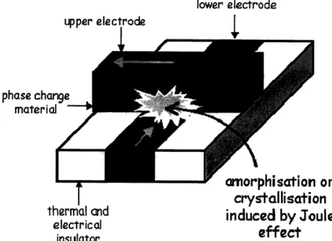
1.3.2 Phase Change Random Access Memory (PCRAM)
Phase Change Memory (PCRAM) comprises of a transistor and a resistor made from chalcogenide material alloys (eg. Ge2Sb2Te5) commonly used in rewritable compact
disks. Electrical charges are used to convert the phase of the material from crystalline, which is conductive, to amorphous, which is resistive, vice versa. This is accomplished though Joule heating. In this way, the resistance state of the material can be used to represent logic '0' and '1'. Multi-state operations can also be achieved by programming the cell to intermediate values. The energy required for phase transformation also decreases with cell size, encouraging memory scaling. Erasable thermal phase change recording at a storage density of 3.3Tb inch"2has been shown and Samsung has produced
a working prototype of PCRAM that is comparable to the size of NOR Flash2 5-26. Issues
include reducing the reset current as cell size scales while maintaining writing capability and reducing thermal cross-talk at higher densitiesl8'28
lower electrode upper electrode phase change material
-&__
I
c
thermal and in electrical insulatorFigure 1.4. Schematic of Phase Change Memory54
or
rystallisation
duced by
Joule
effect
1.3.4 Magnetic Random Access Memory (MRAM)
In Magnetic Random Access Memory, the information is stored as the magnetization direction of ferromagnetic elements. In MRAM, the elements are formed from two ferromagnetic plates, each of which can hold a magnetic field, separated by a thin insulating layer. It utilizes the tunneling magnetoresistive (TMR) effect. The tunneling energy for electrons that are spin-aligned with both magnetic layers is less than that for electrons that are spin-aligned with only one layer. When the orientation of
both magnetic layers is the same, spin-aligned electrons have a higher probability of tunneling through the insulating layer. When the magnetic orientations of the layers are opposed, the tunneling probability of both spin-up and spin-down electrons is reduced. Due to the magnetic tunnel effect, the electrical resistance of the cell changes depending on the orientation of the fields in the two plates. Two plates having the same polarity indicate a logic state of "0", while two plates of opposite polarity indicates a logic state of "1" as resistance is higher. Another type of MRAM consists of two ferromagnetic plates separated by a magnetic, non metallic spacer layer. This utilizes the giant magnetoresistive (GMR) effect. Free electrons are generated 'spin-up' and 'spin-down' in equal proportions. When the orientation of both magnetic layers is parallel, only one type of electron is retarded. When the magnetic orientations of the layers are anti-parallel, both spin-up and spin-down electrons suffer retardation. In this way, resistance is varied to give logic "0" and "1". For both methods, one of the two plates is commonly fixed to one polarity and the other's field will change to match that of an external field29 3 1. Issues with future development of MRAM includes disturbance
from neighbouring cells, stability issues concerning the tunneling barrier and the free layer with increased scalingl8' 31-33
Bit
ItControl
iord
A ZLJ lA L A "IMNIonoltic
ODI IControl 4NEW i~tSjL V./i
Figure 1.5. A MRAM Cell During Read (Above) and Write (Below) Operations34
1.4 Nanocrystal Memory
Another area of active research is the use of nanocrystals to replace a single floating gate as storage sites. This is similar to the use of nitride traps in SONOS memory. It is
easy to integrate nanocrystal based memories into current CMOS processes. It also has several other advantages. This will be discussed further in the next chapter.
References
1. D. Kahng and S.M.Sze "A floating gate ad its application to memory devices," Bell Syst. Tech. J., vol 46, p.1288, 1967
2. Jitu J. Makwana, Dieter K. Schroder "A non-volatile memory overview," http://aplawrence.com/Makwana/nonvolmem.html
3. B.H. Koh et al. "Traps in germanium nanocrystal memory and effect on charge retention: modeling and experimental measurements," J. of Appl Phys, vol 97,
p.124305, 2005
4. Min She and Tsu-Jae King, "Impact of crystal size and tunnel dielectric on semiconductor nanocrystal memory performance," IEEE Trans. On Electron Devices, vol 50, no 9, p. 1934, 2003
5. Ya-Chin King, Tsu-Jae King and Chenming Hu, "MOS Memory Using Germanium Nanocrystals Formed by Thermal Oxidation of Sil.x Ge,," IEEE Electron Devices Meeting, p. 115, 1998
6. Wikipedia, "Flash Memory," www.wikipedia.com.
7. Electronic Information Online, "Flash Memory Devices" http://www.electronics-manufacturers.com/info/computers-and-laptops/flash-memory-devices.html
8. Toshiba, "NAND vs NOR Flash Memory Technology Overview" http://www.chips.toshiba.com
9. Electronics Design, Strategy, News, "What is the difference between NAND and NOR Flash?" http://www.edn.com/article-partner/CA6319916.html
10. Michelle Kessler, "Demand for Flash Memory Skyrockets."
http://www.usatoday.com/money/industries/technology/2005-09-18-flash-memory x.htm
11. Michael Kanellos, " SanDisk drops prices with new flash drives." EETimes Encyclopedia
http://news.com.com/SanDisk+drops+prices+with+new+flash+drive/2100-1041 3-6166983.html
12. Chris Preimesberger, "Hot Flash: 'Flashtops' Take On the Memory Market." eWeek.com http://www.eweek.com/article2/0,1895,2008089,00.asp
13. John Walko, "SanDisk targets gruvi music card at mobiles." EETimes Encyclopedia
http://www.eetimes.com/showArticle.ihtml;jsessionid=ENNZMSCPVD3ZUQSN DLOSKHOCJUNN2JVN?articlelD=171201249
14. Dov Moran, "Progenitor of the USB Flash Drive," EETimes http://www.eetimes.com/showArticle.jhtml;jsessionid=ENNZMSCPVD3ZUQSN DLOSKHOCJUNN2JVN?articlelD = 174401544
15. Theo Valich, "Flash will Kill BluRay ad HD DVD," http://www.theinguirer.net/default.aspx?article=36930
16. Michael Kenellos, "Is Flash Fried?" CNet News.com http://news.com.com/Flash+forward/2009-1040 3-994240.html
17. Aaron Theon and Jean Pierre Leburton, " Towards Single-Electronics," IEEE 2002
18. Betty Prince, "Trends in Scaled and Nanotechnology Memories," Memory Strategies International, IEEE, 2005
19. The International Technology Roadmap for Semiconductors 2006 Update,
Process Integration, Devices and Structures
http://www.itrs.net/Links/2006Update/FinalToPost/04 PIDS2006Update.pdf 20. Jiankang Bu and Marvin H. White, "Design Considerations in Scaled SONOS
Non-volatile Memory Devices"
http:/!klabs.org/richcontent/MemorvContent/nvmt symp/nvmts 2000/presentatio ns/bu white sonos lehigh univ.pdf#search=%22SONOS%20memorv/o22 21. Min She, "Semiconductor Flash Memory Scaling" pHD dissertation, 2003.
22. C.T. Swift et al, "An Embedded 90nm SONOS non-volatile memory utilizing hot electron programming and uniform tunnel erase," IEEE Electron Devices Meeting, p 927, 2002.
23. Dennis A. Adams, David Mavis, James R.Murray and Marvin H.White, "SONOS Non Volatile Memory Semiconductor Memories for Space and Military
Applications."
http://klabs.org/richcontent/MemorvContent/nvmt symp/nvmts 2000/papers/ada ms d.pdf
24. Wikipedia, "Ferroelectric RAM,"
25. Samsung. "Samsung Introduces the Next Generation of Non-Volatile Memory -PRAM,"
http://samsung.com/PressCenter/PressRelease/PressRelease.asp?seq=20060911 0 000286481
26. Hendrik et al. "Ultra-high-density phase-change storage and memory," Nature Vol 5, 383, 2006.
27. PC-RAM Project Home Page http://www.projects.ex.ac.uk/pcram/
28. Yun Sheung Shin. "Non-volatile Memory Technologies for Beyond 2010," 2005 Symposium for VLSI Circuits Digest of Technical Papers, 2005
29. IBM, "IBM Research News",
http://www.research.ibm.com/resources/news/20001207 mramimages.shtml 30. Phillips Password Magazine, "MRAM- Magnetic Memory Goes Solid State",
http://www.research.philips.com/password/archive/12/mram.html
31. S. Tehrani et al, "Progress and Outlook for MRAM Technology", IEEE Transactions on Magnetics, Vol 35, No 5,p 2814, 1999
32. Johan Akerman, "Towards a Universal Memory", Science Vol 308, p508, 2005. 33. W.J. Gallagher et al. "Recent Advances in MRAM Technology, " IEEE VLSI
Technology, p72-7 3 2005. (VLSI-TSA-Tech).
34. J.P. Nozieres, "Magnetic random access memories (MRAM): a truly universal memory?" Unpublished Paper
Chapter 2: Nanocrystal Memory
Nanocrystal memory has been an area under intense research since Tiwari et al. demonstrated a Si nanocrystal memory that uses direct tunneling into three dimensionally confined nanocrystals for bi-stability in the conduction of a transistor channell'2. Since then, memory effects of materials such as Germanium-8 3 and transition metals such as Au, Ag, W, Pt and Sn9-3 have been investigated by various research groups worldwide.
2.1 Nanocrystal Memory Device
The memory devices demonstrated by Tiwari et al. are based on a Flash memory structure (consisting of a MOSFET as illustrated in Figure 1) with floating islands of silicon nanocrystals embedded in the gate oxide. This is illustrated in Figure 4. By using electrically isolated charge storage sites, charge leakage via localized oxide defects is reduced and a superior retention time can be achieved. As a result, a thinner tunneling oxide can be employed. This relaxation in the tunneling oxide constraint results in smaller operating voltages as well as lower power dissipation than current Flash EEPROM. It also brought about faster programming and at low operating voltage via direct tunneling mechanisms.1'2 Nanocrystal based memories are also
more resistant to defects in the tunnel oxide. In addition, nanocrystal based memories are less complex to manufacture than conventional Flash memory. Conventional
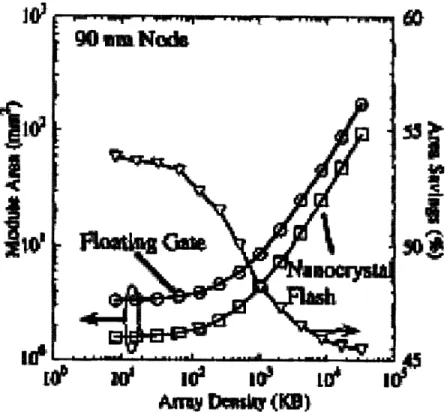
memory requires 11 additional mask adders over the basic CMOS process while nanocrystal memory requires only 4. The reduction in complexity is due to the elimination of process steps to satisfy the high voltage requirements in conventional Flash memory. The removal of high voltage requirements in nanocrystal memory also enable nanocrystal memory to scale better than conventional Flash memory. This is evident from Figure 2.2. Germanium as well as metal-nanocrystal-based transistors work similarly to silicon nanocrystal memory.
I1
alt lwd
Figure 2.1: Schematic of Silicon Nanocrystal Based Memory
U U I l
Process Step Logic Floating Gate Nanocrystal Isolation Formation
High Voltage Wells 2 masks
NVM Array Well (lMask) 1 mask lmask
Tunnel Oxidation
Floating Gate Deposition/Patterning 1 mask
ONO/Nanocrystal Dep./Patterning 1 mask 1 mask
Low Voltage Wells OGO Wells
High Voltage Oxidation/Patteming I mask 1 mask
OGO Oxidation Patterning Low Voltage Oxide CGrowth Gate Deposition
NVM Stack Patterning 1 mask
NVM Source Hole Implant I mask
NVM Drain Implant I mask I mask
Gate Patterning
High Voltage LDD Implants 2 masks
OGO LDD Implants S/D and Backend Processing
Masking Step Adder +11 +4
Taken from:
R. Muralidhar et al, "A 6VEmbedded 90nm Silicon Nanocrstal Non-volatile Memory",
IEEE Int Conf, 31, 2004
Table 2.1 Mask adders required to integrate nanocrystal based non volatile memory into a standard CMOS flow compared against conventional non volatile
IW
Ll"
AnM
D
mie (KD)
Figure 2.2: Memory module size for both conventional nanocrystal based NVM showing approximate factor of two based NVM'4
I5
I
floating gate NVM and reduction for nanocrystal
2.2 Synthesis of Germanium Nanocrystals
There are numerous ways of synthesizing germanium nanocrystals. These include cosputtering5-7, chemical vapour deposition15
-17, ion implantation3,4, sol gel techniques1" oxidation and reduction of SiGe films19and molecular beam epitaxy20.
int3cbaionJ~j~
I
steady-ta-te~~ regimte nucleationsequilibrium
saturation coarsening
regime regime
Figure 2.3: Schematic illustration of the density of supercritical particles as a function of time after quenching.21
Figure 2.3 shows a schematic illustration of the density of supercritical particles as a function of time after quenching. It can be observed that there are 4 stages of growth; namely, incubation, steady-state nucleation, equilibrium saturation and coarsening. In the incubation regime prior to the nucleation stage, the incubation time can be obtained by extrapolating the steady-state nucleation slope to zero density. In the nucleation stage, the steady-state nucleation rate can be predicted from the slope of the curve in this steady-state regime. Nanocrystals form by nucleation and growth.
The density of the particles peaks in the equilibrium saturation regime. Subsequently, coarsening or ripening of the particles occurs, where a decrease in the particle density is observed. In this stage, the supersaturation of the matrix with respect to the solute atoms is sufficiently small to make nucleation of new particles unlikely. Ostwald ripening (coarsening) of nanocrystals will then occur.
The nanocrystal size is usually controlled by time and annealing temperature. In the coarsening phase, the Lifshitz-Slyozov theory of coarsening in alloys is normally used to describe the time evolution of the sizes of the particles of a phase coarsening by mass transfer among particles in a matrix. The Lifshitz-Slyozov-Wagner (LSW) theory predicts the rate of coarsening in alloys. It states that at large times t, the critical dimension xc tends asymptotically to depend on time as t'13. At the same time,
the degree of supersaturation correspondingly falls as ft"3 and the number of grains as
t-1 . Large particles grow while smaller ones shrink at the coarsening stage due to the Gibbs Thomson effect. The Gibbs-Thomson effect relates the curvatures of the spherical grains (represented by rl and r2) to their corresponding activities
(represented by al and a2) and hence solubilities in solution by the following
equation:
RTln(-) = 2Vm[o[1
-a, r2 r,
R and T are the molar constant and the temperature, respectively. Vm represents the molar volume of a certain phase and a represents the interfacial energy between two phases. The difference in the solute concentrations for different curvature particles
sets up a concentration gradient that drives diffusion of matter from the smaller to the larger particles 21,22
The material in which Ge nanocrystals are embedded is usually SiO2 although
other types of materials such as A1203 are also investigated in research projects23.
2.3 Characterization of Nanocrystals
A variety of structural, optical and electrical techniques are commonly used to
characterize Ge nanocrystals.
For structural characterization, transmission electron microscopy (TEM) is commonly used. It enables the size distribution, the spatial distribution, shape and defect structure of the nanocrystals to be studied. X-ray photoelectron spectroscopy is commonly used to investigate the chemical bonds that are present while Raman spectroscopy is used to determine the crystallinity and size of the nanocrystals. In addition, secondary ion spectroscopy (SIMS) allows a quantitative depth profiling of the elements in a sample.
The most commonly used characterization method is photoluminescence (PL) spectroscopy, especially in the study of quantum confinement effects. For electrical
methods, capacitance-voltage (C-V), capacitance-time (C-t) and current-voltage (I-V), measurements can be made to characterize the charge storing capability of nanocrystal-based transistor devices.
2.4 Charge Storage in Nanocrystal Memory Devices
There is an argument going on in the research community on the way in which nanocrystals store charge. It has been suggested that the charges are stored at the conduction band 1,2,24 or at deep traps 7,8,25. Recent research indicates that charges are
more likely linked to interfacial traps. Y.Shi et al. has highlighted that the band edge of a Si nanocrystal is higher than that of the substrate due to three dimensional quantum confinement effects. As a result, any electrons stored in the conduction band can easily tunnel back to the substrate. This cannot account for the observation of long retention times. He proposed that the injected electrons are stored at deep traDping sites.
1.0
0.8
x0.6
0 0.4
0.2
non
-5 -4 -3 -2 -1 0 1 2 3 4 5Gate Voltage
[v]
10l l1p 100n
E Ion
C in 1p lIOp In -2 -1 0 1 2 3 4 5 - 6Gate Voltage [v]
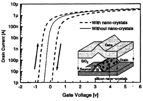
Figure 2.4: C-V hysteresis loops for various annealed MOS capacitors. The inset is a schematic of the MOS memory structure based on silicon nanocrystals 2 .
In order to investigate the effect of traps on charge storage, Shi et al. annealed various MOS capacitors in an H2 ambient at 430 °C and in vacuum at 700 OC. The
former process effectively decreased the number of interface traps by H-passivation, and the latter resulted in a high density of interface traps, especially Pb centers. Figure 2.4 shows the C-V characteristics for the treated samples as well as the as deposited ones. The device annealed in vacuum exhibited the largest Vfb shift as it has the highest trap density. The minimum Vfl shift is observed for the H2 annealed device
having the lowest trap density. This means that more charges are stored in the nanocrystals synthesized by annealing in vacuum rather than in H2.
A A 2.0 -0.5 --o
C
-1.0
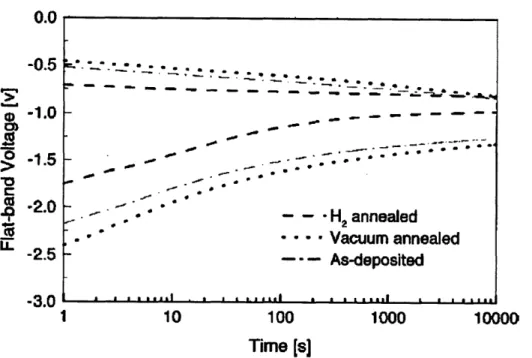
LS--2.5 30 1 10 100 1000 10000 Time [s]Figure 2.5: Long-term charge retention characteristics in various annealed MOS capacitors, measured using the constant-capacitance method at the flat-band point 25
Figure 2.5 shows the long-term charge storage characteristics of various devices where the changes in the net charge stored in nanocrystals are proportional to the shifts of the Vfb obtained under constant-capacitance conditions. The fastest rate of electron loss is observed for the vacuum-annealed device while the H2-annealed device has the slowest electron-loss rate. Therefore, a higher rate of charge loss is obtained for a device with a higher density of traps. Furthermore, the temperature dependence of the charge storage characteristics shows that the charge-loss rate decreases slightly when the temperature changes from 300 K to 80 K. This implies
O-P
• .~
*._-H
annealedS Vacuum annealed
- - - As-deposited
aE
m--AaAias-
d aAl i aaaepthat thermal activation is not dominant for the charge-loss processes in the tested samples.
Efs
Efm
Tunneling
Si 2
Gate SiO
2Figure 2.6: Energy band diagram of the MOS memory structure at flat-band condition for electron tunneling processes in the retention mode after injecting electrons 25
Based on the above experimental results, Shi et al proposed a model whereby an injected electron will first fill up the empty states in deep trap levels prior to filling up shallower trap levels. There are two mechanisms in which electrons can be detrapped and lost to the silicon substrate. The first is direct tunneling from the traps to the interface states at the SiO2/Si interface (process 2). Charge loss by this mechanism
can be reduced by reducing number of interface states. The second is the indirect process involving the thermal detrapping of electrons to the conduction band (process 3) and then tunneling back to the substrate (process 1). A deeper trap level is
desirable for suppressing this kind of thermal activation. Shi et al. concluded from the experimental observation of charge loss rates on interface trap density and temperature that process 2 determines the long term charge retention in the samples. He further notes that the traps and defects at the internal/surface of nanocrystals and the interface states at the SiO2/Si substrate play different roles in the charge-loss process. The traps and defects at the internal/surface of a nanocrystal determine the amount of charge that can be stored. On the other hand, a smaller number of the interface states in the Si/SiO2 interface would effectively result in a lower tunneling
rate and longer retention time 25
Chen et al also concluded that at least some of the electrons are stored in traps after comparing experimental results with simulation data generated by another research group 8,26
Unlike Shi et a125, King27 and Koh et al.28 note a significant temperature dependence in their Ge nanocrystal memory samples. Like Shi, they demonstrated that the memory devices lose their memory effect after annealing in a hydrogen ambient, thus showing that charges are stored in the interfacial traps rather than in the conduction band. Koh et al 28 found good agreement of experimental data with
simulations (Figure 2.6). The simulated data was based on the temperature dependent Shockley-Read-Hall (SRH) relationship developed by McWhorter et al. 29. The thermal equilibrium emission constant of electrons can be derived as
e, = AT 2 exp(-qE, /kT),
where k is the Boltzmann constant, q is the electronic charge, T is the temperature, Et is the trap energy level measured with respect to the conduction edge of the nanocrystal and A is the temperature independent constant which can be expressed as
4 t60'gk2m . m is the effective mass of the electron, g is the degeneracy and
h is Planck's constant. Also, the drain current during the discharge phase is modeled as
IDS(trans,ent) = q{n [1 - exp(-.t)] + n2 [1- exp(1 -
exp(-A2t]
},
where n, + n2 = n and n is the total number of nanocrystalline Ge charging sites. X1
and X2 represent the discharging rate constants for the two different discharging
mechanisms. 8.0X10⁴ -2.OxlOO
-
4.OxlO-2010
0,o~0~ 1 10 100 time (s) S 100-766Cm~r 100t
10m
100 -F ý) r 9··CT ___~_ 50C; -.- ... ... . ....,0- - -M
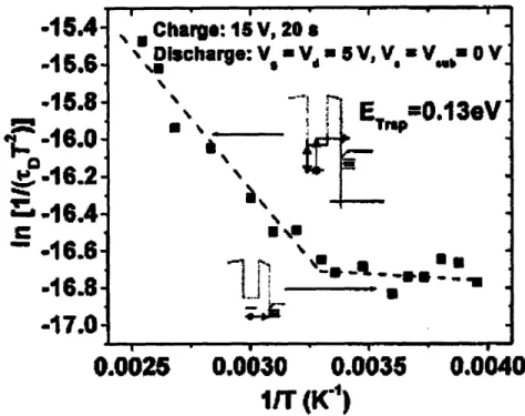
'' T ·II *Figure 2.7: Drain current (IDs) transient at a read voltage of 5V after a write operation at 15V for 20s. The symbols represent the measured data and the lines are fitted data from a simulation. The increase in Dlos for higher temperatures could be
explained by the larger carrier mobility and the higher intrinsic carrier concentration of the substrate.28
By performing transient drain current (IDs) measurements, the trap energy levels (Et) can be extracted. This is done by performing transient drain current measurements at different temperatures and calculating the discharging time constant
(TD). TD is defined as the time corresponding to 90% of the IDS at steady state, when
the drain current gradually returns to steady state value. The electrons which are detrapped during the discharge phase increase the drain current over its steady sate value. Figure 2.8 indicates that for the samples, below 307.7K, the discharging process is relatively temperature insensitive, which corresponds to Process 2 (direct tunneling from the traps to the interface states at SiO2/Si interface) as described by
Shi et al. Above 307.7K, Process 1 + 3 (indirect process involving the thermal detrapping of electrons to the conduction band and then tunneling back to the substrate) is more dominant and the discharging process shows a strong temperature dependence.28
15.4•16.0
-W-16.2
-16.8
-17.0
0.
0025
0,0030
0.0035
1lT (K")
Figure 2.8: Inverse of discharging time constant (Y ) divided by the square of the
temperature plotted against the inverse of T. The graph is plotted based on the calculations given by RD oc e, = AT2 exp(-qE, / kT). RD is the rate of discharge.28
Based on the above research observations, the following conclusions can be made:
1. The discharge process is dominated by Process 1 + 3 at high temperatures and Process 2 at low temperatures.
2. At low temperatures, decreasing the interface state at SiO2/Si substrate interface
will improve retention time. 25
S
Ch
arge:
15, 20
a
% Discharge:
V =V,
=
5VO,
V
W
V
04
o
V
1S=0.13eV
nsp ~ rr I ·1. 5, -NO %-WO %a0.0040
--4 |0025
3. At high temperatures, controlling the deep level traps is crucial to increase the retention duration of the memory device. Engineering the trap energy level can be carried out by manipulating the material of the host matrix, doping with impurities or changing the material of the tunnel oxide. The last method is based on the assumption that the trap sites in the nanocrystals responsible for charge storage are close to the Si substrate and such trap sites are affected by the close proximity to the tunnel barrier. Koh et al were able to prove this by showing that that nc-Ge/Al203 has higher activation energies and hence deeper trap levels than
nc-Ge/SiO2. 28 Other than methods involving increasing trap levels, retention time can also be increased by increasing the tunnel barrier, such as using germanium/silicon (Ge/Si) heteronanocrystals, which will be discussed later.
ft.^
Ur
t
3
S5,Nanocrystal Diameter (nm)
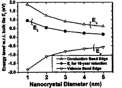
Figure 2.9: Trap energy level required for 10 year charge retention performance vs nanocrystal diameter. The Ge band-gap widening due to quantum confinement effect is also indicated. The conduction and valence bands edges at the boundaries of the
widened Ge band gap are given by Ec and Ev. (Ec- Ed = (Ej- Ev)=0.33eV in bulk Ge,
E, is the midgap energy of Ge.28
Figure 2.9 illustrates the trap energy required to meet the 10 year requirement taking into account quantum size effects28. We can see from Figure 2.9 that as the size of nanocrystals decrease, Ec-Et increases, and deeper level traps are required. As the size of the nanocrystals decreases, the barrier height is lower and it is easier for the electrons to leak through the tunnel barrier. In order to compensate for this,
deeper-level traps are required.
It is important to note that there is a tradeoff between read/write speeds and voltages with retention time. The thicker the tunnel oxide, the longer the retention time, the lower the operating speeds and the higher the voltages required. By improving retention time through other means, such as trap level engineering, read/write voltages can be decreased and operating speeds improved by decreasing the oxide barrier. Hence, other attributes such as operating speeds and voltages are inextricably linked to retention time.
2.5 Optimum Nanocrystal Size
There is also a tradeoff between the reliability/memory window with the retention time/programming speed. Generally, there is a need to fabricate nanocrystals as small
as possible in order to increase memory window and to reduce stress induced leakage during retention to improve reliability.
However, when the nanocrystals decrease, retention time is degraded as quantum confinement effects become significant. Confinement effects are strongly dependent on nanocrystal diameter and scales inversely with the square of nanocrystal diameter. In addition, coulomb blockage effects of small nanocrystals decrease tunneling probabilities and reduce programming speed. Coulomb charging effects are inversely proportional to the nanocrystal diameter. The two effects are evident from Figure 2.10. Retention time degrades as nanocrystal diameter decrease from 5nm to 2nm. Also, programming time is faster for 5nm diameter nanocrystals compared to 2nm diameter nanocrystals.
Neglecting effects of stress-induced leakage, we will attempt to estimate the largest nanocrystals that satisfy the minimum memory window requirements. The larger the size of the nanocrystals, the smaller the quantum confinement and coulomb blockage effects.30 32
0 0
1010
·
iol
0iI0
101
20
22
24
26
28
30
tunnel ode tic
(A)
Figure 2.10: Retention characteristics at various tunnel oxide thicknesses and the Ge nanocrystal size on device performance30
'I
Tunnel oxide thickness [nm]
Figure 2.11: Plot of threshold voltage shfifs A VT and retention period r, as afunction of tunnel oxide thickness.3'
Referring to Figure 2.11, for a ten year retention period, a tunnel oxide thickness of 3nm is required. This corresponds to a AVT of around 0.1V. This value can be used in the following equation
Q,
AV,
= -R
Q1
C
,
where R is a factor correcting for the non uniform coverage of the area by discrete nanocrystals (assumed to be 0.4), Q' is the total charge density stored and C' is the nanocrystal-gate capacitance per unit area.32 Also,
C,=
C1= 6
t
where s is the dielectric constant of the interpoly silicon oxide dielectric and is given by 3.9 x 8.854 x 10-12 F / m and t is the interpoly silicon oxide thickness (assumed to be 6nm).32 Assuming that one nanocrystal on average stores one charge,
Q'=-Ne
= C'xA VT _ 5.755 x 10-3 x0.1R 0.4
N= 9x10⁵ / m2 = 9x10" l /cm 2
N is the nanocrystal density (N=9x10 15/m2 =9x101 1/cm2 ) and e is the
EwJ
19 t.-
4I8
9-z 0.4- : 02
E....
I. I. Ii . * 0 10 20 30 40 50 60Depositin time (soc)
Figure 2.12: Nucleation curve for nanocrystal deposited by CVD on SiO2 showing the
evolution of nanocrystal density and size with deposition time.33
Based on the above assumptions, the optimum nanocrystal size is 3nm. However, it must be :noted that the optimum size is determined by factors such as the tunnel and
interpoly oxide thickness as well as the method in which the nanocrystals are deposited (the nucleation curves for other methods of deposition, such as sputtering, may differ from that of CVD).
47
Figure 2.13: OrderedArray ofNanocrystals
If the nanocrystals are deposited in an ordered array as shown above, then
A=-I=1.11x10⁻⁶m2 N
L = \ = 1.05 x 10-'m
Assuming that the spacing between the nanocrystal is equal to the nanocrystal diameter, then
L
D = - = 5.27 x 10⁻⁹ m = 5.27nm
2
2.6 Comparison of Different Nanocrystal Memories
I
I---I I I I I I I I I I I., I I I I I I I
---- ---
I
-'-"
The earliest work on quantum-dot Flash memories concentrated on nanocrystalline silicon (nc Si) as a replacement for the floating gate. Since then, numerous groups have proposed using nanocrystalline germanium (nc Ge) and metal dots such as Au, Ag, W, Pt, and Sn 9-13. The main advantages of using metal nanodots include a higher density of states around the Fermi Level, making them more immune to Fermi Level fluctuations caused by contamination and ensuring tighter threshold voltage control, and the creation of an asymmetrical barrier by engineering the work function and thus inducing a smaller barrier for writing and a larger barrier for retention. The potential well of the metal nanocrystals can be carefully engineered to yield a small barrier for writing and a large barrier for retention. The use of different types of metal nanocrystals with different work functions opens the possibility of changing the barrier height by 2eV.9 However, the
introduction of metal nanodots to current silicon processing technology is a great challenge. It is well known that the presence of contaminants vastly affects the performance of the transistor and an in-depth feasibility study needs to be undertaken before metal nanodots can be introduced to the baseline CMOS process. 10 Also, most of the advantages of metal nanocrystals revolve around improving the retention time. This can be achieved through other means using semiconductor nanocrystal memories also as highlighted above.
There are no in-depth experimental studies comparing the performance of silicon and germanium nanocrystal memory devices. However, researchers have pointed out some theoretical advantages of Ge nanocrystals over Si. Ge has a smaller bandgap
compared to Si, which results in a higher confinement barrier for retention similar to metal nanocrystals.34 Retention time could also be improved, especially if electrons detrap by Process 1+3 as highlighted above.
2.7 Hetero-nanocrystal Memory
A novel MOSFET memory storage cell using Ge/Si hetero-nanocrystals has been proposed35. Simulation results show that the hetero-nanocrystals have superior charge retention capability compared to Ge and Si nanocrystals alone. Ge has a smaller bandgap than Si and by introducing a Si interface around the nanocrystal, it would create an additional barrier height at the Ge/Si interface which makes it harder for electrons to leak out. A staircase potential well is created and charges will have to pass through both the potential barrier of Si nanocrystal and the tunnel barrier before it can leak out. During writing and erasing, the movement of charges is mainly affected by only the potential barrier of the tunnel oxide under the proper bias. Hence, the retention time could be prolonged remarkably while the writing and erasing time could be held to be approximately the same order of magnitude.3 5
- Camnu=Incdry.ta
,-- .Coisteelide
1-(a)
(b)
Figure 2.14: (Left) The schematic cross sectional of Ge/Si heteronanocrystal memory
half cell. (Right) The valence band diagram for (a) hole writing (b) retention and (c)
erasing. It is the effect of the compound barrier that prolongs the retention time of device evidently.35
Two ways in which heteronanocrystal memories can be fabricated are: (1) using porous alumina and (2) using diblock copolymers.
Porous alumina after first anodization in oxalic acid
Removal of porous alumina layer by phosphoric and chromic
acid Initiation of hole formation in second
anodization
Hole formation in second anodization
Coating of protective layer eg. PMMA
(a)
( b)
(d)
Removal of Al layer in saturated HgCI2solution
bRemoval
of bottom layer (a) using phosphoric acid4, (h) 0 0 0
30nm 4'
Removal of protecting layer using acetone
Evaporation of nanocrystal material on
SiO2 through mask
Nanocrystal array on Si
Fig 2.15: Fabrication of ordered nanocrystal array using porous alumina using a two step anodization process. The first anodization serves as a template for ordered hole formation in the second anodization.36
· 1
700
0C
NOW Si Nanocrystals111L
Ge Nanocrystals OR GeEtch and anneal
Ge Si
Fig 2.16: Formation of heteronanocrystals using porous alumina.
Fig. 2.15 illustrates one of the methods for fabricating porous alumina membranes. The fabricated alumina membrane can then be used for the ordered
1111111
10000C
deposition of heteronanocrystals or serve as masks for etching as shown in Figure 2.16. Experiments carried out using Ge nanodots show a highly ordered array.3
Figure 2.17: High magnification view of Ge nanodot array fabricated using alumina membrane.37
Diblock copolymers have been used for the ordered deposition of Si nanocrystals.3 8 It is likely that these could be extended to heteronanocrystals.
pomm Om7O
rri r"
M M M M1
r-"Z
h onnk
,o n.o ,Program CxW* rAnocrystst 7Growing of oxide and
spin coating + phase
separation of polymer
solution to promote
phase separation
Etching of oxide
Growing of program
oxide to form tunnel
barrier + deposition of
amorphous Si
RIE of amorphous Si +
annealing for
formation of Si
nanocrystals
Figure 2.18: Ordered formation of silicon nanocrystals using diblock copolymers.38
PMMA
Diblock
copolymers of
PMMA and
polystrene
polystyrene
0.6 styrene+ 0.4
methyacrylate
0.6 styrene+ 0.4
methyacrylate + TEMPOinitiator
Figure 2.19: Schematic for formation of vertical blocks ofpolystyrene.39
, Prca


![[PDF] Les portails : créer et gérer un site web](data:image/gif;base64,R0lGODlhAQABAIAAAP///wAAACH5BAEAAAAALAAAAAABAAEAAAICRAEAOw==)