HAL Id: hal-02492335
https://hal.laas.fr/hal-02492335
Submitted on 26 Feb 2020
HAL is a multi-disciplinary open access
archive for the deposit and dissemination of
sci-entific research documents, whether they are
pub-lished or not. The documents may come from
teaching and research institutions in France or
abroad, or from public or private research centers.
L’archive ouverte pluridisciplinaire HAL, est
destinée au dépôt et à la diffusion de documents
scientifiques de niveau recherche, publiés ou non,
émanant des établissements d’enseignement et de
recherche français ou étrangers, des laboratoires
publics ou privés.
silicon: from optical properties to vacancy-mediated
dopant diffusion
G Herrero-Saboya, L. Martin-Samos, Antoine Jay, Anne Hémeryck, N.
Richard
To cite this version:
G Herrero-Saboya, L. Martin-Samos, Antoine Jay, Anne Hémeryck, N. Richard.
A
comprehen-sive theoretical picture of E centers in silicon: from optical properties to vacancy-mediated dopant
diffusion. Journal of Applied Physics, American Institute of Physics, 2020, 127 (8), pp.085703.
�10.1063/1.5140724�. �hal-02492335�
A comprehensive theoretical picture of E centers in silicon:
from optical properties to vacancy-mediated dopant diffusion
G. Herrero-Saboya,1, 2,a) L. Martin-Samos,3 A. Jay,2A. Hemeryck,2 and N. Richard1
1)CEA, DAM, DIF, F-91297 Arpajon, France
2)LAAS-CNRS, Université de Toulouse, CNRS, Toulouse, France
3)CNR-IOM/Democritos National Simulation Center, Istituto Officina dei Materiali, c/o SISSA, via Bonomea 265, IT-34136 Trieste,
Italy
(Dated: 5 February 2020)
Among the common vacancy-related point defects in silicon, the E center is one of the most prominent due to its degrad-ing effect in silicon-based technology. Even though it has been the subject of extensive experimental and theoretical studies, a comprehensive theoretical model capable of reproducing the experimental evidence for all three dopants (P, As and Sb) is still missing. Guided by a Jahn-Teller model, we are able to reproduce the absorption bands and the transi-tion probability between equivalent geometries of the defect at low temperatures by including many-body-perturbatransi-tion corrections based on the GW approximation on top of DFT. At higher temperatures, vacancies become mobile centers, allowing the reorientation of the whole defect and contributing to the dopant diffusion. The underlying mechanisms of vacancy-mediated dopant diffusion are revisited, characterizing the activation energies of such technologically relevant processes, obtaining quantitative results in good agreement with experiment.
I. INTRODUCTION
One of the most abundant point-like defects in n-type doped silicon is the E center. It consists of a silicon vacancy trapped next to a donor element (most commonly P, As and
Sb). Besides their known electronic activity1, E centers
can play important roles in specific performance losses and long term degradation processes. The phosphorous-vacancy complex (also denoted as the PV center) is postulated, for instance, to be at the origin of the two level Dark
Current-Random Telegraph Signal2–5in image sensors, since
the defect reorientation at room temperature is believed to cause the variation of the measured conductivity. The arsenic-vacancy (AsV) and antimony-vacancy (SbV) com-plexes, are considered crucial in dopant diffusion as the vacancy-mediated contribution seems to be comparable to or
even higher than the interstitial-mediated mechanism6. The
possibility for a center to exhibit and/or participate to the aforementioned phenomena relies strictly on the details of its potential energy surface (PES) and the underlying reaction mechanisms that could be activated.
E centers were first characterized by Watkins and Corbett during a series of Electronic Paramagnetic Resonance (EPR)
studies of point defects in silicon7,8. They reported that the
ground state configuration of the neutral E center presents a pairing geometry: one of the three interatomic distances between the three silicon atoms adjacent to the vacancy is shorter than the other two, see Figure 1. Moreover, in 7 and 8 two temperature regimes were distinguished. At low temperature stress measurements revealed the existence of
three degenerate ground state geometries (P1, P2 and P3 in
Figure 1b), separated by an energy barrier of 60-70 meV.
Later optical absorption studies9 of PV−, AsV− and SbV−
a)Corresponding author. Email: gherrero@laas.fr
showed a ground state Jahn-Teller distortion of opposite sign. In this configuration, known as resonant, one of the silicon bonds is longer than the other two (see Figure 1). The change of Jahn-Teller distortion with the charge state, together with the presence of degenerate ground states was explained by a
simple single-electron orbital model10, according to which
the PES is predicted to exhibit the form of a Mexican hat.
Furthermore, Watkins hypothesized10that the energy barrier
between equivalent minima for the neutral systems actually corresponds to the energy difference between pairing and
resonant configurations. At higher temperatures, energy
barriers of 0.90 up to 1.30 eV, for P, As, Sb were observed. Such barriers were assigned to the reorientation of the vacancy-dopant axis, i.e. the reorientation of the whole vacancy-dopant complex. It was also postulated that this re-orientation process, followed by a dopant-vacancy exchange would characterize the vacancy-mediated dopant diffusion.
On the modelling side, the energy ranking of these
con-figurations is not consistent between different studies11–16:
the ground state geometry for the PV center was found to be a pairing configuration for both neutral and negative charge states in [11] (see also Ref. 12 for the neutral charge state) but a resonant one in [13]. Later studies reported a rather flat PES with multiple metastable minima, comprising pairing, resonant and, in some cases, also breathing (B)
configurations14,15. Only for the AsV center the measured
Jahn-Teller distortion at neutral and negative charge states (pairing and resonant distortions respectively) has been
correctly reproduced16. In all the aforementioned works, the
assessment for metastability has been only based on total energy calculations with no further exploration of the actual PES shape. This leaves the question open about the ground state geometry and low-temperature behavior of the E center in silicon, and of the capacity of computational modelling to
reproduce experimental findings7,8.
In the present work, by means of state-of-the art DFT-based
This is the author’s peer reviewed, accepted manuscript. However, the online version of record will be different from this version once it has been copyedited and typeset.
R P
P
P
P
R
R
R
1 3 2 3 2 1 Sb, As, P 1 2 31
2
3
defect axis d 1 2 3 12 13 d23B
B
dFIG. 1. The silicon E center: its projection along the vacancy-dopant axis (a) and Watkins et al. model for its potential energy surface at the neutral charge state (b). Three geometries for the E center are dis-tinguished depending on the relative interatomic distances between atoms 1, 2 and 3: the symmetric breathing configuration (B), the pairing configuration (P), and the resonant-bond configuration (R). Piand Ridenote the pairing and resonant geometries with unpaired
distances djk<di j=dikand djk>di j=dik, respectively.
methods we obtain the ground state geometry for different
charge states, in line with Watkins et al. observations7–9. The
presence of Jahn-Teller distortions is further confirmed by accurately describing and analyzing the electronic structure of vacancy-dopant complexes by means of many-body perturbation theory within the GW approximation. The PES shape is explored by single-point total energy calculations on interpolated geometries and by using Climbing Image
Nudged Elastic Band (CI-NEB)17. Within this approach,
we are able to reproduce the model proposed by Watkins et al.: three pairing degenerate minima and three resonant degenerate saddle points, with the higher energy maximum breathing mode lying at the top of the Mexican hat potential (see Figure 1b).
Finally, by using the CI-NEB algorithm we found energy barriers for the reorientation of the whole vacancy-dopant complex in very good agreement with the experimental mea-surements. For the exchange mechanism, for which no di-rect experimental measure is available, our results suggest a rethinking of this diffusion mechanism: the barrier, higher
than what previously postulated7,8, seems to indicate a
rele-vant vacancy-mediated contribution only for the case of Sb. However, in contrast with Ref. [18], we still find the presence of a positive, if small, barrier.
II. COMPUTATIONAL DETAILS
Structural properties are obtained by means of the Density Functional Theory (DFT) as implemented in the ABINIT
code19. All reported results are based on the 216/215 atoms
supercell. The Brillouin zone is sampled at gamma. The
ONCVPSP norm-conserving pseudopotential20 and the
Perdew-Burke-Ernserhof exchange-correlation functional21
have been chosen. An energy cutoff for the plane wave basis set of 762, 1306 and 1225 eV has been employed for the PV, AsV and SbV centers, respectively, resulting in a total energies convergence below 0.5 meV, for the complexes em-bedded in silicon bulk. Defect geometries at different charge states have been optimized by means of the BFGS algorithm, with a convergence threshold of 1 meV/Å. All geometries discussed in the present manuscript were obtained without any symmetry constrain. ABINIT, as all plane-wave codes, includes a compensating background charge for all charged systems. In addition, we also, turned on Markov-Payne
corrections22.
Real space electronic densities obtained by means of DFT
are plotted using the XCrySDen package23.
The PES is explored by both the climbing-NEB method17
as implemented in ABINIT, with a mean total energy conver-gence threshold of 1 meV, and by single-point total energy calculations.
Many-body corrections are computed on top of the
Kohn-Sham energies within the GW method (G0W0as implemented
in the ABINIT code19,24) in order to obtain the defect band
structure correctly. We employ the Godby-Needs plasmon-pole model and a cutoff energy of 82 eV to describe the dielectric matrix. In order to assure convergence of the GW exchange-correlation self-energy, we use a very large ratio of 10:1 empty bands versus occupied bands. Spin-unrestricted calculations are performed for the neutral charge state.
III. GROUND STATE ELECTRONIC STRUCTURE: CONFIRMATION OF THE JAHN-TELLER MODEL
The geometry of the point defect at different charge states is characterized by the interatomic distances between atoms 1, 2 and 3 in Figure 1 (or the vacancy’s first silicon neighbors). We report a pairing configuration (P in Figure 1)
as the ground state for the PV0, AsV0and SbV0centers and
a resonant geometry (R) for the negative charge states, in
agreement with the experimental evidence7–9. The breathing
mode configuration (B in Figure 1) is the ground state for the three centers at positive charge state (or empty trap), in
agreement with previous hypothesis10. The characteristic
interatomic distance, di j, for PV+, AsV+and SbV+is equal
to 3.54 Å, 3.59 Å and 3.63 Å respectively. The increase of the interatomic distance with the dopant atomic number is due to the subtle relaxation of the dopant towards the vacant site;
This is the author’s peer reviewed, accepted manuscript. However, the online version of record will be different from this version once it has been copyedited and typeset.
going from its ideal substitutional site to a slight interstitial position. The dopant net displacement at positive charge state is equal to 0.06 Å, 0.22 Å and 0.43 Å, in ascending order of the dopant atomic number. Such tendency is observed for all charge states, with a lower absolute displacement for 0 and -1 cases due to the increase of electronic density at the vacant site. Such behavior is not visible by EPR spectroscopy, it does however have an important implication on the impurity diffusion mechanism, as discussed in later sections.
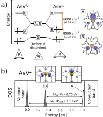
The change in structural configuration or Jahn-Teller distortion with the charge state can be explained through the electronic occupation of the trap-induced levels. By means of a simple one-electron molecular orbital (MO) model, the
electronic configuration of the E center was described10 as
a linear combination of the three dangling bonds a1, a2and
a3, located in atoms 1, 2 and 3 respectively. In the case of
the breathing mode configuration, i. e. before the Jahn-Teller distortions, the lowest electronic level corresponds to the
high symmetric state S = (a1+a2+a3)/√3, whereas states
A = (2a1− a2− a3)/√6 and B = (a2− a3)/√2 are higher
and degenerated in energy (see Figure 2a). If the empty trap gets occupied by one or two electrons, the system undergoes a structural reconfiguration in the form of a Jahn-Teller distortion, breaking the degeneracy of states A and B. The
state A is favored by the pairing configuration, P, (εA<εB),
whereas the state B is lower in energy in the case of the resonant, R, configuration. A simple MO model is able to predict, for example, that at neutral charge state the unpaired electron is mainly located at one of the silicon neighboring atoms (atom 1 in Figure 2a), as described by state A and
observed by EPR spectroscopy7,8. It is however limited to the
description of localized levels, overlooking the presence of bulk delocalized states, and to the use of empirical parameters when estimating the relative position of the trap levels. The splitting of the defect levels A and B after the spontaneous
distortion was confirmed by optical absorption experiments9
on the AsV− center, where two absorption bands were
reported at 0.74 eV and 1.05 eV. They were assigned to electronic excitations from an occupied localized state (S and B levels in Figure 2) to the unoccupied state A. Unfortunately, no values for the other two dopants were reported. However, Watkins speculated that their defect-induced optical bands
should be very similar to AsV−. Even though the electronic
structure of the E center is a clear evidence of the Jahn-Teller effect, no quantitative description has so far been given due to
the limitations of previously used mean-field approaches11–16.
Our DFT calculations qualitatively reproduce the point defect electronic structure obtained by means of simple symmetry arguments; i.e. the degeneracy of levels A and B in the absence of Jahn-Teller distortions and the splitting and reversion of such levels for the pairing and resonant configurations. Moreover, the electronic density distributions of the Kohn-Sham states A and B are in good agreement with the simple MO model (see Figure 2). The inclusion of crystal field effects, in contrast with Watkins’ simple MO model, allows us to determine that the highly symmetric S
S AsV
_
(1.05 eV) (before JT distortion) (0.74 eV) Ener gy A 1 3 2 B 1 3 2 6000 cm 8500 cm -1 -1 AsV0 P R A, B A B A BB
0.0 0.2 0.4 0.6 0.8 1.0 A B DOS Energy [eV] V alence band Conduc tion ba ndb)
0.70 eV A B EA - IP = 1.03 eV A TVB EA - IP =AsV
-a)
FIG. 2. Watkins’ single-electron molecular orbital model8,10 (no
crystal field effects included), before and after Jahn-Teller (JT) dis-tortions, measured optical bands9and their corresponding
electronic-transition assignments within Watkins’ model for AsV− (a).
Com-puted GW density of states for AsV at negative charge state is plot-ted in (b). Calculaplot-ted optical absorption bands (EAA-IPBand EAA
-IPTVB) for the AsV−center9and their assignment to single-particle
electronic transitions. In addition, the electronic density of the DFT-corresponding A and B states is also shown. DFT-DFT-corresponding Watkins’ S state is strongly hybridized with the valence states.
state does not appear as a disentangled localized state, but it hybridizes with the silicon bulk states, becoming part of the valence band for all charge states (and it is therefore not represented in Fig. 2b). Defect-induced levels A and B are always found to be within the forbidden silicon band. On the other hand, the electronic state coming from the donor atom is completely disentangled from both bulk states and localized trap states S, A and B; it is located deep in the valence band, at approximately 0.5 eV from the top of the valence band. In order to provide a quantitative description of the band structure, many-body perturbation corrections in
the GW approximation25,26are computed on top of the DFT
eigenvalues. In Figure 2b, we show the quasi-particle Density Of States (DOS) for the E center embedded in silicon. The semiconductor band gap (defined as the difference between the first electronic affinity and the first ionization potential of the bulk, i.e. the bottom of conduction band and the top of
the valence band, EABCB− IPTVB) is in agreement with the
experimental value of 1.17 eV.
As the electron-hole interaction is small, because of the
high macroscopic dielectric constant of silicon (ε∞∼ 12.0),
quasi-particle energy differences between empty and
occu-This is the author’s peer reviewed, accepted manuscript. However, the online version of record will be different from this version once it has been copyedited and typeset.
pied states (ionization potentials and electronic affinities) can be exploited to meaningfully estimate vacancy-dopant-complex-related optical absorption bands. In the case of the
AsV−center, see Figure 2, the energy difference between the
first ionization potential (IPB) and the first electronic affinity
(EAA) can be assigned to the 6000 cm−1(0.74 eV) absorption
peak reported in [9], confirming that such transition occurs from the occupied defect state B to the unoccupied localized
state A. In the case of the 8500 cm−1(1.05 eV) band, we
as-sign the measured absorption band to an electronic excitation involving the top of the valence band and the localized level A
(here described as EAA- IPTVB). We remark that the previous
assignment made by Watkins was limited to a MO model, and therefore the position of the top of the valence band was ne-glected from the electronic structure prediction (see Figure 2).
TABLE I. First excitations energies within many-body perturbation theory in the form of the GW approximation for the E center at charge states 0, ± 1. A and B stand for the localized defect states, whereas TVB stands for the top of the valence band.
Charge
state PV CenterAsV SbV
+ 1 EAA,B− IPTVB 0.59 – 0.60 – 0.49 –
0 EAEAB− IPA 0.66 – 0.62 – 0.56 –
B− IPTVB 0.88 – 0.85 – 0.75 –
-1 EAEAA− IPB 0.72 0.76a 0.70 0.74a 0.60 0.68a
A− IPTVB 1.04 – 1.03 1.05a 0.89 –
aMeasured absorption bands9
We estimate the absorption bands for PV− and SbV− to
be located at 0.72 eV and 1.04 eV and 0.60 eV and 0.89 eV respectively (see Table I), confirming that the E center has similar electronic properties independently of the dopant, as postulated in [9]. The predicted optical absorption bands at charges states 0 and +1 are also given in Table I
IV. LOW TEMPERATURE REGIME:
THE MEXICAN HAT ENERGY SURFACE
We now focus our attention on the energy landscape of the
E center at low temperatures, studied by EPR stress studies7,8
in the case of the neutral charge state. As hypothesized by
[7 and 8], we found three pairing configurations, P1, P2and
P3 in Figure 3a, as ground state minima of the potential
energy surface (Pi is characterized by an unpaired distance
djk <di j=dik). The unpaired electron is therefore mainly
located in silicon atom i at the pairing configuration Pi (see
the form of the localized state A in Figure 2). Even though the three distortions are geometrically equivalent, the elec-tronic jumps between atoms 1, 2 and 3 modify the magnetic moment of the center, making the transitions between pairing
configurations visible through EPR spectroscopy7,8. The
lifetime of each distortion was estimated by compressing the bulk in a given spatial direction (prioritizing one of the three orientations) and studying the recovering time of the
back-reorientation. The low-temperature regime reorientation
barriers were estimated to be within 60-70 meV7,8 and it
was later postulated10 that such energy barriers actually
correspond to the energy difference between the pairing and the resonant geometries. A NEB calculation between points
P1and P2finds the R3geometry (resonant configuration
char-acterized by unpaired distance d12>d31=d32) as the saddle
point of the transition path, proving Watkins hypothesis regarding the height of the energy barriers between equivalent minima. We estimate the energy difference between pairing and resonant configurations to be 36 meV, 31 meV and 28
meV for PV0, AsV0and SbV0respectively. As in Ref. [16]
the "disagreement" between the calculated barrier, 20 meV
for the AsV0complex, and the measured value8, 70 meV, was
attributed to size effects, we performed calculations on a 511 atoms supercell. We obtained a very similar value of about 38 meV for all three dopants, showing that size effects are particularly important for the SbV complex.
The potential energy surface for the E center at neutral charge state is, therefore, characterized by three pairing geometries as degenerated minima, separated by three resonant configurations as saddle points (see Figure 3a). Along the Minimal Energy Path (MEP), despite structural changes between pairing and resonant configurations seem "negligible", the unpaired electron localizes at different atomic sites (see the electronic density plots that follow the
symbolic paths P1→ R3→ P2in Figure 3 a). At the saddle
point, the system adopts a resonant configuration for which the half-filled electronic orbital becomes state B, as expected from a Jahn-Teller system (see Figure 2 a). If we consider a set of configurations along a straight path between a pairing and resonant configurations with the same characteristic unpaired distance, the system is forced to pass through a high symmetric configuration, close to the breathing mode geometry (B in Figure 1), overcoming an energy barrier of ∼ 60-100 meV (see figure 3 (b)). According to the above results, the PES of the E-center exhibits, therefore, the shape of a Mexican hat, in agreement with Watkins ideas and measurements. At room temperature, the barriers between
pairing configurations are comparable to kBTRT and the
neutral E center can reorient by circling around the Mexican hat. For the negative charged E centers the Mexican hat is inverted: pairing and resonant configurations become, respectively, saddles and minima points. The energy barriers to jump from one minimum, R configuration, to another
one is of 62 meV, 48 meV and 25 meV for PV−, AsV−
and SbV− respectively (511 atoms supercell) at the DFT
level of approximation. As in the neutral case, size effects are important when computing such reorientation barrier, resulting in up to 20 meV energy difference between 215 and 511 silicons supercells. Positively charged E centers exhibit a single minimum that corresponds to the breathing configuration, B.
The systematic underestimation of the barriers, 40 meV for all three dopants, against the 60 to 70 meV measured
by Watkins et al.7,8, is a signature of the well known
This is the author’s peer reviewed, accepted manuscript. However, the online version of record will be different from this version once it has been copyedited and typeset.
P P R R R 1 1 2 2 3 Reorientation process for PV0
a)
b)
20 40 60 0 80 100 R1 P1 E n e rgy [m e V] P3 P1 R3 2 P 1 2 3 P1 R1 PV AsV SbV 0 0 0~B
P1 R3 Energy [meV] 20 40 30 0 10 PV AsV SbV 0 0 0B
BFIG. 3. Transition mechanism between pairing configurations, P, (a) and potential energy surface (b) of E centers at neutral charge state. The electronic density for the unpaired electron at different atomic configurations is also shown. Points are obtained within the CI-NEB algorithm (a) and single point DFT calculations (b). Lines are a guide for the eye.
Self-Interaction problem in standard DFT exchange and correlation functionals. A combined DFT-GW approach, as previously exploited to correct total energy differences in
point-defects studies27,28, is here used to correct barriers as
follows. By definition, the ionization potential computed
within the GW method for the pairing configuration (RP) at
neutral charge state can be written as a total energy difference,
IP (RP, 0) = E (RP, 0) − E (RP, +). By computing the same
quantity at the resonant configuration, the reorientation
barrier at neutral charge state can be written as,∆E (RP,RR;
0) = IP (RP, 0) − ∆E (RP,RR; +) − IP (RR, 0). The quantity
∆E (RP,RR; +) is the difference in energy between the pairing
and resonant configurations at positive charge state (empty trap) and therefore can be safely estimated within DFT. In the case of the PV center (where the elastic contributions are minimal at 216 atoms), such difference in ionization
potentials, IP (RP, 0) − IP (RR, 0), is equal to 65 meV and
the corresponding reconfiguration energy, ∆E (RP,RR; +),
is 10 meV, given an overall reorientation barrier of 75 meV. Similarly, a value of 71 meV is obtained for the AsV center.
V. HIGH TEMPERATURE DYNAMICS:
VACANCY-DOPANT COMPLEX REORIENTATION AND EXCHANGE
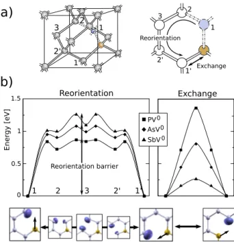
The present section is dedicated to the two mechanisms
underlying the vacancy-mediated dopant diffusion: the
defect reorientation and the vacancy-dopant exchange (see Figure 4a). The first process involves the reorientation of the vacancy-dopant axis, through the movement of the vacancy to second (vacancy positions 2 and 2’ in Figure 4a) and third neighbor positions (denoted 3) with respect to the impurity. Such mechanism was first proposed by [7 and 8], after performing EPR stress studies at high temperatures. They obtained the lifetime of each defect-axis orientation, corre-sponding to activation energies that were comprised between 0.9 and 1.3 eV, for dopant-increasing atomic number. As in the case of low temperature studies, a characterization of the
atomic process and its energy landscape at high temperatures is possible by EPR spectroscopy due to the change in mag-netic moment between the initial and final configurations (see configurations 1 and 1’ in Figure 4b). It was also postulated that the reorientation mechanism constituted the bottleneck process for vacancy-mediated diffusion, since the energy expense for the dopant-vacancy exchange was believed to be close to 0.33 eV (activation energy for the monovacancy
diffusion in silicon29).
The high temperature dynamics of the E center is studied through the mechanisms of defect reorientation and
dopant-vacancy exchange within the CI-NEB algorithm17. The
exchange of positions between the dopant and the vacancy is a direct symmetric process, as shown in Figure 4b. The decrease of the energy barrier with the increase of the dopant size is explained by the ground state geometry of the E center. As mentioned in section III, the dopant slightly moves from its ideal substitutional position towards the vacant site. Such effect increases with the dopant size, as it is evident by the low energy barrier obtained, in particular, for the antimony-vacancy exchange. In contrast with the simple exchange process, the reorientation of the defect axis, requires the movement of the vacancy to different sites of the lattice before arriving to its final configuration. In order to compute the Minimal Energy Path between equivalent positions 1 and 1’, a preliminary study of transient geometries is required. Geometry relaxation calculations were made for the vacancy at second and third neighbor positions from the dopant in or-der to specify the beginning and ending points of consecutive NEB calculations (see Figure 4b). Two different minimal energy paths are therefore characterized (1 → 2 and 2 → 3), with their respective energy barriers. The relative stability of the second neighbor and third neighbor configurations present opposite tendencies with the dopant size. The E center is barely stable at third neighbor configuration in the case of
the PV0center, finding an energy barrier of 26 meV, whereas
the energy expense to leave such configuration is about 0.16 eV in the case of the antimony. As it is shown in Figure 4b, such behavior is inverted in the case of the second neighbor
This is the author’s peer reviewed, accepted manuscript. However, the online version of record will be different from this version once it has been copyedited and typeset.
configuration, obtaining energy barriers to return to the first
neighbor site of 11 meV for SbV0and 0.11 eV for PV0. The
reorientation barrier observed by EPR stress studies at high
temperatures7,8 is here estimated as the energy difference
between the ground state configuration of the E center and the saddle point of the 2 → 3 transition (see Figure 4).
1 3 1' 2' 2 1 1' 2' 3 2 Exchange Reorientation
a)
1 2 3 2' 1' 1.5 1 0.5 0 E n e rgy [e V]b)
PV AsV SbV 0 0 0 Exchange Reorientation Reorientation barrierFIG. 4. The vacancy-mediated dopant diffusion mechanisms: the reorientation of the defect and the exchange vacancy-dopant (a) and their computed energy landscapes (b). The probability density for the unpaired electron along both processes is shown. Only relevant points, corresponding to local minimum and saddle points, are shown in the case of the reorientation process. Lines are guides to the eye.
The theoretical values obtained in Table II clearly show that the diffusion of the whole vacancy-dopant complex is energet-ically more expensive in the case of the PV center than pos-tulated by Ref. [7] from the mono-vacancy diffusion. While a detailed study of the diffusion mechanism of the E center is beyond the scope of the present work, our results indicate that vacancy-mediated diffusion would be the primary diffu-sion mechanism for large dopant-atomic numbers, as it has been experimentally proved in Ref. [6].
VI. CONCLUSIONS
In conclusion, we provide a comprehensive theoretical picture of the silicon E center comprising structural, elec-tronic and optical properties, together with their low- and high- temperature behavior, that ultimately complies with experiments.
The electronic ground state of the silicon E center is explained through a symmetry-based Jahn-Teller model:
the trap-induced states can recombine to lower the defect energy by distorting the symmetric breathing geometry into a pairing configuration (at neutral charge state) or resonant configuration (negative charge state). The relative position of these localized states (states A and B in Figure 2), can be ac-curately reproduced by many body perturbation calculations within the GW approximation. The calculated defect-related optical absorption bands are located at 0.70 eV and 1.03 eV
for the AsV− complex and at 0.72 eV and 0.60 eV for the
PV− and SbV− centers, in very good agreement with the
measured bands at 0.74, 1.05, 0.76 and 0.68 eV respectively. First-principles studies beyond the DFT method confirm that the E center presents similar optical and electronic properties independently of the dopant.
Thanks to an exhaustive first-principles exploration of the E center PES, we confirm that it exhibits the shape of a Mexican hat, in agreement with Watkins et al measurements. We find three degenerate pairing configurations (P in Figure 1) as
ground state for PV0, AsV0 and SbV0 separated by three
resonant (R in Figure 2) configurations as saddle points. Such centers are therefore not metastable as it was reported and/or
inferred in previous theoretical calculations14,15. At negative
charge state the resonant configuration becomes the minima of the sombrero, while the pairing configurations become unstable. The energy barriers encountered at low tempera-tures between equivalent minima are correctly estimated only when the electronic interaction is treated accurately within the GW approximation.
At higher temperatures, we explore the energy landscape for the vacancy-dopant axis reorientation, finding activation energy barriers in very good agreement with experiments. Moreover, the computed exchange barriers offer a new insight on the vacancy-mediated diffusion. In particular, in the case of the SbV complex, they support the long time belief that Sb diffuses in silicon mainly through a vacancy-mediated mech-anism.
1P. Pichler, Intrinsic point defects, impurities, and their diffusion in silicon
(Springer Science & Business Media, 2012) Chap. 5.
2I. H. Hopkins and G. R. Hopkinson, “Further measurements of random
tele-graph signals in proton irradiated CCDs,” IEEE Transactions on Nuclear Science42, 2074–2081 (1995).
3D. Smith, A. Holland, and I. Hutchinson, “Random telegraph signals in
charge coupled devices,” Nuclear Instruments and Methods in Physics Re-search Section A: Accelerators, Spectrometers, Detectors and Associated Equipment530, 521 – 535 (2004).
4T. Nuns, G. Quadri, J. David, and O. Gilard, “Annealing of proton-induced
random telegraph signal in CCDs,” IEEE Transactions on Nuclear Science 54, 1120–1128 (2007).
5C. Virmontois, V. Goiffon, P. Magnan, O. Saint-Pe, S. Girard, S. Petit,
G. Rolland, and A. Bardoux, “Total ionizing dose versus displacement damage dose induced dark current random telegraph signals in cmos image sensors,” IEEE Transactions on Nuclear Science58, 3085–3094 (2011).
6A. Ural, P. B. Griffin, and J. D. Plummer, “Fractional contributions
of microscopic diffusion mechanisms for common dopants and self-diffusion in silicon,” Journal of Applied Physics85, 6440–6446 (1999), https://doi.org/10.1063/1.370285.
7G. D. Watkins and J. W. Corbett, “Defects in irradiated silicon: Electron
paramagnetic resonance and electron-nuclear double resonance of the Si-E center,” Phys. Rev.134, A1359–A1377 (1964).
This is the author’s peer reviewed, accepted manuscript. However, the online version of record will be different from this version once it has been copyedited and typeset.
TABLE II. Exchange barriers, first neighbors binding energies and reorientation barriers at high temperatures for PV0, AsV0and SbV0. Values
are given in eV. T.W. stands for this work, whereas O. W. stands for other works.
Dopant Exchange barrier binding energy1st neighb. Reorientation barrier
T. W. O. W. T. W. O. W. T. W. O. W. Exp.
P 1.36 1.0518, 1.2930 0.84 1.0518 0.87 0.830 0.937
As 0.81 0.6518 0.95 1.1718 1.07 1.016 1.078
Sb 0.26 -0.0518 1.01 1.4518 1.26 – 1.288
8E. L. Elkin and G. D. Watkins, “Defects in irradiated silicon: Electron
para-magnetic resonance and electron-nuclear double resonance of the arsenic-and antimony-vacancy pairs,” Phys. Rev.174, 881–897 (1968).
9G. D. Watkins, “Optical properties of group-V atom-vacancy pairs in
sil-icon,” Radiation Effects and Defects in Solids111-112, 487–500 (1989), https://doi.org/10.1080/10420158908213023.
10G. Watkins, “Understanding the Jahn–Teller distortions for the divacancy
and the vacancy–group-V-atom pair in silicon,” Physica B: Condensed Mat-ter376-377, 50 – 53 (2006), proceedings of the 23rd International Confer-ence on Defects in Semiconductors.
11R. Virkkunen and R. Nieminen, “First-principles study of the
phosphorous-vacancy pair in silicon,” Computational Materials Science1, 351 – 357 (1993).
12G. Pfanner, C. Freysoldt, J. Neugebauer, and U. Gerstmann, “Ab initio
EPR parameters for dangling-bond defect complexes in silicon: Effect of Jahn-Teller distortion,” Phys. Rev. B85, 195202 (2012).
13M. G. Ganchenkova, A. Y. Kuznetsov, and R. M. Nieminen, “Electronic
structure of the phosphorus-vacancy complex in silicon: A resonant-bond model,” Phys. Rev. B70, 115204 (2004).
14A. N. Larsen, A. Mesli, K. Bonde Nielsen, H. K. Nielsen, L. Dobaczewski,
J. Adey, R. Jones, D. W. Palmer, P. R. Briddon, and S. Öberg, “e center in silicon has a donor level in the band gap,” Phys. Rev. Lett.97, 106402 (2006).
15M. Ganchenkova, L. Oikkonen, V. Borodin, S. Nicolaysen, and R.
Niem-inen, “Vacancies and E-centers in silicon as multi-symmetry defects,” Ma-terials Science and Engineering: B159-160, 107 – 111 (2009), eMRS 2008 Spring Conference Symposium K: Advanced Silicon Materials Research for Electronic and Photovoltaic Applications.
16S. Ö˘güt and J. R. Chelikowsky, “Charge state dependent Jahn-Teller
distor-tions of the E-center defect in crystalline Si,” Phys. Rev. Lett.91, 235503 (2003).
17G. Henkelman, B. P. Uberuaga, and H. Jónsson, “A climbing image
nudged elastic band method for finding saddle points and minimum en-ergy paths,” The Journal of Chemical Physics113, 9901–9904 (2000), https://doi.org/10.1063/1.1329672.
18J. S. Nelson, P. A. Schultz, and A. F. Wright, “Valence and atomic size
de-pendent exchange barriers in vacancy-mediated dopant diffusion,” Applied Physics Letters73, 247–249 (1998), https://doi.org/10.1063/1.121779.
19X. Gonze, F. Jollet, F. Abreu Araujo, D. Adams, B. Amadon, T.
Applen-court, C. Audouze, J.-M. Beuken, J. Bieder, A. Bokhanchuk, E. Bousquet, F. Bruneval, D. Caliste, M. Côté, F. Dahm, F. Da Pieve, M. Delaveau, M. Di Gennaro, B. Dorado, C. Espejo, G. Geneste, L. Genovese,
A. Gerossier, M. Giantomassi, Y. Gillet, D. Hamann, L. He, G. Jo-mard, J. Laflamme Janssen, S. Le Roux, A. Levitt, A. Lherbier, F. Liu, I. Lukaˇcevi´c, A. Martin, C. Martins, M. Oliveira, S. Poncé, Y. Pouillon, T. Rangel, G.-M. Rignanese, A. Romero, B. Rousseau, O. Rubel, A. Shukri, M. Stankovski, M. Torrent, M. Van Setten, B. Van Troeye, M. Verstraete, D. Waroquiers, J. Wiktor, B. Xu, A. Zhou, and J. Zwanziger, “Recent de-velopments in the ABINIT software package,” Comput. Phys. Commun. 205, 106–131 (2016).
20D. R. Hamann, “Optimized norm-conserving Vanderbilt pseudopotentials,”
Phys. Rev. B88, 085117 (2013).
21J. P. Perdew, K. Burke, and M. Ernzerhof, “Generalized gradient
approxi-mation made simple,” Phys. Rev. Lett.77, 3865–3868 (1996).
22G. Makov and M. C. Payne, “Periodic boundary conditions in ab initio
cal-culations,” Phys. Rev. B51, 4014–4022 (1995).
23A. Kokalj, “Xcrysden—a new program for displaying crystalline structures
and electron densities,” Journal of Molecular Graphics and Modelling17, 176 – 179 (1999).
24F. Bruneval, N. Vast, and L. Reining, “Effect of self-consistency on
quasi-particles in solids,” Phys. Rev. B74, 045102 (2006).
25L. Hedin, “New method for calculating the one-particle Green’s function
with application to the electron-gas problem,” Phys. Rev.139, A796–A823 (1965).
26L. Hedin and S. Lundqvist, “Effects of electron and
electron-phonon interactions on the one-electron states of solids,” (Academic Press, 1970) pp. 1 – 181.
27P. Rinke, A. Janotti, M. Scheffler, and C. G. Van de Walle, “Defect
forma-tion energies without the band-gap problem: Combining density-funcforma-tional theory and the GW approach for the silicon self-interstitial,” Phys. Rev. Lett.102, 026402 (2009).
28L. Martin-Samos, G. Roma, P. Rinke, and Y. Limoge, “Charged oxygen
de-fects in SiO2: Going beyond local and semilocal approximations to density
functional theory,” Phys. Rev. Lett.104, 075502 (2010).
29G. Watkins, “An EPR study of the lattice vacancy in silicon,” J. Phys. Soc.
Japan18, Suppl. II, 22 (1963).
30X.-Y. Liu, W. Windl, K. M. Beardmore, and M. P. Masquelier,
“First-principles study of phosphorus diffusion in silicon: Interstitial- and vacancy-mediated diffusion mechanisms,” Applied Physics Letters 82, 1839–1841 (2003), https://doi.org/10.1063/1.1562342.
31H. Xu and U. Lindefelt, “Electronic structure of vacancy-phosphorus
im-purity complexes in silicon,” MRS Proceedings163, 287 (1989).
This is the author’s peer reviewed, accepted manuscript. However, the online version of record will be different from this version once it has been copyedited and typeset.
R
P
P
P
P
R
R
R
1
3
2
3
2
1
Sb, As, P
1
2
3
1
2
3
defect axis
d
1
2
3
1
2
13
d
23
B
B
d
This is the author’s peer reviewed, accepted manuscript. However, the online version of record will be different from this version once it has been copyedited and typeset.
S
AsV
_
(1.05 eV)
(before JT
distortion)
(0.74 eV)
Ener
gy
A
1
3
2
B
1
3
2
6000 cm
8500 cm
-1
-1
AsV
0
P
R
A, B
A
B
A
B
B
0.0
0.2
0.4
0.6
0.8
1.0
A
B
DOS
Energy [eV]
V
alence
band
Conduc
tion
ba
nd
b)
0.70 eV
A
B
EA - IP =
1.03 eV
A
TVB
EA - IP =
AsV
-a)
This is the author’s peer reviewed, accepted manuscript. However, the online version of record will be different from this version once it has been copyedited and typeset.
P
P
R
R
R
1
12
23
R e o rie n ta tio n pr oc e ss for PV 0a
)
b)
2 0 4 0 60 0 801
00
P
1En
ergy
[me
V]
P
3
P
1R
3 2P
1
2
3
P
1
R
1
PV
AsV
S
bV
0 0 0~B
P
1
R
3
E n e rgy [m e V] 2 0 4 0 30 10 0 PV AsV SbV 0 0 0B
B
This is the author’s peer reviewed, accepted manuscript. However, the online version of record will be different from this version once it has been copyedited and typeset.
1
3
1
'
2
'
2
1
1
'
2
'
3
2
E
xc
h
a
n
ge
R
e
o
rie
n
ta
tio
n
a
)
1
1
'
2
3
2
'
1
.5
1
0.5
0
En
ergy
[eV]
b)
PV
AsV
S
bV
0
0
0
E
xc
h
a
n
ge
R
e
o
rie
n
ta
tio
n
R
e
o
rie
n
ta
tio
n
ba
rr
ie
r
This is the author’s peer reviewed, accepted manuscript. However, the online version of record will be different from this version once it has been copyedited and typeset.