Control of a Semiconductor Dry Etch Process using
Variation and Correlation Analyses
by
Tan Nilgianskul
B.S. Materials Science and Engineering
Cornell University (2015)
Submitted to the Department of Mechanical Engineering
in partial fulfillment of the requirements for the degree of
Master of Engineering in Manufacturing
at the
MASSACHUSETTS INSTITUTE OF TECHNOLOGY
September 2016
© 2016 Massachusetts Institute of Technology. All rights reserved.
Author . . .
Department of Mechanical Engineering
August 19, 2016
Certified by . . .
Duane S. Boning
Professor of Electrical Engineering and Computer Science
Thesis Supervisor
Accepted by. . .
Rohan Abeyaratne
Quentin Berg Professor of Mechanics
Chairman, Department Graduate Committee
Control of a Semiconductor Dry Etch Process using Variation
and Correlation Analyses
by Tan Nilgianskul
B.S. Materials Science and Engineering Cornell University (2015)
Submitted to the Department of Mechanical Engineering on August 19, 2016 in partial fulfillment of the requirements for the degree of
Master of Engineering in Manufacturing
Abstract
Statistical process control (SPC) is one of the traditional quality control methods that, if correctly applied, can be effective to improve and maintain quality and yield in any manufacturing facility. The purpose of this project is to demonstrate how to effectively apply SPC to a dry etch process (in this case plasma ashing), at Analog Devices, Inc., a company that runs large-scale fabrication sites in the Boston area. This thesis focuses on spatial and run-to-run variation across multiple measurement sites on a wafer and validates the assumptions of normality and correlation between sites within a wafer in order to justify and confirm the value of employing SPC theories to the plasma ashing process. By plotting control charts on past data, outlier data points are detected using Analog’s current monitoring system. Further, irregularities in the process that would not have been detected using traditional x-bar Shewhart charts are detected by monitoring non-uniformity. Finally, cost analysis suggests that implementing SPC would be a modest investment relative to the potential savings.
Thesis Supervisor: Duane Boning, Professor of Electrical Engineering and Computer Science
Acknowledgements
I would like to thank Prof. Duane Boning and Prof. David Hardt for advising us on process control theories throughout this project. I would like to thank Ken Flanders and Jack Dillon, heads of the process engineering and manufacturing operations teams, for providing close technical guidance and for their supervision throughout our time working at Analog Devices, Inc. Furthermore, all the experimental work done leading up to this thesis would not have been possible if not for other process engineers in the etch group including Pamela Petzold, Peter Cardillo, Rich DeJordy, Dale Shields along with many others who were of great support in performing experiments the cleanroom. I would also like to thank Dr. Brian Anthony for initiating this collaboration between MIT and Analog Devices and Jose Pacheco for coordinating with all parties involved
throughout the M.Eng. program.
Finally, I would like to especially thank my project teammates, Tanay Nerurkar and Feyza for their contribution to the work presented in this thesis as well as for their incredible support throughout the entire course of this program.
Table of Contents
Abstract ...3 Acknowledgements ...4 List of Figures ...7 List of Tables ...9 1. Introduction ...101.1 Background Information on Analog Devices, Inc. ...10
1.2 General Semiconductor Fabrication Process. ...11
1.3 Plasma Ashing Process. ...12
1.3.1 Gasonics Aura 3010 Plasma Asher ...13
1.3.2 Partial and Forming Recipes ...15
1.3.3 Data Collection and Logging ...17
1.3.4 Calculation of Basic Statisics ...19
2. Theoretical Review of Key Concepts ...23
2.1 Statistical Process Control (SPC) ...23
2.1.1 Origin of SPC ...23
2.1.2 Shewhart Control Charts ...23
2.2 Analysis of Variance ...25
2.3 Design of Experiments ...26
2.4 Hypothesis-Testing ...29
2.4.1 Z-Test for Detecting Mean-shifts ...29
2.4.2 F-Test ...31
2.4.3 Bartlett’s Test ...32
3. Statistical Process Control: Methodology ...34
3.1 Source of Data ...34
3.2 Test for Normality ...34
3.3 Fundamental Analysis Procedure ...36
4.1 Raw Shewhart Charts ...38
4.1.1 Analog’s Original Run Charts ...38
4.1.2 Three Sigma Control Charts ...39
4.1.3 Principle Component Analysis ...41
4.2 Separation of Variation Components ...44
4.3 Additional Modified Parameters to Monitor ...45
4.3.1 Weighted Average Thickness ...45
4.3.2 Non-Uniformity ...45
5. Benefits for Analog Devices, Inc. ...50
5.1 Choosing “Control Groups” ...50
5.1.1 Monitoring Weighted Average Thickness ...51
5.1.2 Monitoring Non-Uniformity ...54
5.2 Recap of Possible Paths to Take ...58
5.3 Cost-Benefit and Tradeoffs ...61
5.3.1 Cost-Benefit and Tradeoffs ...61
5.3.2 Comparing the Costs of Three Options ...62
5.3.3 Recommendations ...63
6. Conclusions and Future Work ...65
6.1 Conclusions ...65
6.2 Suggestions for Further Studies ...66
References ...67
List of Figures
Figure 1-1: ADI’s manufacturing facilities. ...11
Figure 1-2: Semiconductor processing steps [4]. ...12
Figure 1-3: Ashing process schematic [5]. ...13
Figure 1-4: Gasonics Aura 3010 machine [7]. ...14
Figure 1-5: Display-screen of Gasonics tool [6]. ...15
Figure 1-6: Spatial distribution and coordinate positions of the nine sites. ...18
Figure 1-7: Data logging from Nanospec 9200. ...19
Figure 2-1: Example of a Shewhart control chart. ...24
Figure 3-1: Histogram of the nine-site average thickness from G53000 ...35
Figure 3-2: Normal probability plot of nine-site average from G53000. ...36
Figure 4-1: Original control chart on G53000. ...39
Figure 4-2: Shewhart x-bar control chart with control limits calculated using the average nine-site standard deviation as 𝑠. ...41
Figure 4-3: Data from site 2 plotted against data from site 3. ...42
Figure 4-4: Weighted average thickness run chart. Grand mean and ±3σ calculated based on all 127 runs. ...46
Figure 4-5: WIWNU run chart. ...48
Figure 5-1: WAT control limits calculated from the lumped nine months of data. ...52
Figure 5-2: WAT control limits calculated from samples 45 to 60. ...53
Figure 5-3: WAT control limits calculated from samples 64 to 89. ...54
Figure 5-4: WIWNU control limits calculated from the lumped nine months of data. ....56
Figure 5-5: WIWNU control limits calculated from samples 40-70. ...57
Figure 5-7: three methods in setting control limits. ...59 Figure A1: Control limits for WAT calculated from the lumped nine months of data
under the forming recipe. ...70
Figure A2: Control limits for WIWNU calculated from the entire nine months of data
under the forming recipe. ...71
Figure A3: Control limits for WIWNU calculated from the samples 50 through 80 under
List of Tables
Table 1-1: Machine parameters for the Partial recipe. ...16
Table 1-2: Machine parameters for the Forming recipe. ...17
Table 2-1: 23 full factorial experimental design. ...28
Table 2-2: 23-1 factorial experimental design. ...28
Table 4-1: Variance distribution across nine principle components. ...43
Table 4-2: Process variance broken down into the within-wafer or “error” component and the between-wafer or “group” component. ...44
Table 4-3: ANOVA table to test the significance of spatial variation. ...45
Table 5-1: Parameters and results for the F-test done on WAT of samples 45-60 vs. samples 64-89. ...52
Table 5-2: Parameters and results for the t-test done on WAT of samples 45-60 vs. samples 64-89. ...52
Table 5-3: Parameters and results for the F-test done on the WIWNU of samples 40-70 vs. samples 98-111. ...55
Table 5-4: Parameters and results for the Z-test done on the WIWNU of samples 40-70 vs. samples 98-111. ...56
Table 5-5: Summary of maintenance costs. ...62
Chapter 1: Introduction
The work in this thesis presents a methodology to systematically perform statistical process control on a high volume semiconductor dry etch process. It lays out the necessary tools required to build statistical regression models and demonstrates potential implications and analyses that could be used to better understand, monitor and ultimately improve the performance of the machines involved. This is an industrial thesis, and the work was done in collaboration with Analog Devices Inc. (will also be referred to as ADI or Analog) at their fabrication facility in Wilmington, MA. Analog Devices Inc. is a world leader in the design, manufacture, and marketing of high performance analog, mixed-signal, and digital signal processing integrated circuits used in a broad range of electronic applications. The company is headquartered in Norwood, MA. Currently, there is a need in the company to rigorously analyze various processes and machine
capabilities in an effort to improve yield, throughput, and reduce machine downtime. The rest of this chapter will provide background information on Analog Devices Inc. as well as an introduction to the semiconductor dry etch process that was studied in this work. Finally, the chapter ends by explicitly stating the problem statement will be addressed later on throughout this thesis.
1.1
Background Information on Analog Devices Inc.
Analog Devices Inc. is an American multinational company that specializes in the design, manufacturing, and marketing of high performance analog, mixed-signal, and digital signal processing integrated circuits used in a broad range of electronic
applications. The company’s products play a fundamental role in converting,
conditioning, and processing real-world phenomena such as temperature, pressure, sound, light, speed and motion into electrical signals that would be then used in a wide array of electronic devices.
The company was founded in 1965 by Ray Stata and Matthew Lorber. It has operations in 23 countries and serves over 100,000 customers ranging from those in the consumer electronics and automotive industry to the defense industry. Analog’s revenue
The manufacturing and assembly of ADI’s products is conducted in several locations worldwide. Figure 1-1 shows an overview of the location and functions of the company’s manufacturing and assembly facilities.
Figure 1-1: ADI’s manufacturing facilities.
This experiments in this thesis were carried out on a dry etch process in the Wilmington, MA fabrication center. This thesis is written in conjunction with the works of Feyza Haskaraman and Tanay Nerurkar, and several sections and descriptions in this thesis are written in common with their works [2, 3].
1.2 General Semiconductor Fabrication Process
Pre-doped wafers are supplied to the Wilmington fabrication site as the starting material. The Wilmington fabrication site is divided into five main sub-departments: thin-films, etch, photolithography, diffusion and CMP (chemical mechanical polymerization). A key procedure used at many points in the manufacturing of a device is
photolithography where photoresist is deposited and patterned onto desired parts of the wafer. This allows the diffusion team to selectively implant impurity ions, the etch group to remove materials, or the thin-films group to deposit metals onto the designated parts of the silicon wafer. Afterwards, the etch group strips the resist off from these wafers. The
function of the CMP group is then to use chemical-mechanical reaction techniques to smoothen the surface of the deposited materials.
Figure 1-2: Semiconductor processing steps [4].
Different types of devices will require a different set and configuration of material layers, with repeated sequences of photolithography, etch, implantation, deposition, and other process steps. In fact, the flexibility of this process setup enables ADI to produce customizable electronic parts on a customer’s short-term order.
1.3 Plasma Ashing Process
For the purpose of this thesis, the plasma ashing process is investigated. This process is used to remove photoresist (light-sensitive mask) from an etched wafer using a monoatomic reactive species that reacts with the photoresist to form ash, which is
removed from the vicinity of the wafer using a vacuum pump. The reactive species is generated by exposing a gas such as oxygen or fluorine to high power radio or
microwaves, which ionizes the gas to form monoatomic reactive species. Figure 1-3 shows a general schematic of the plasma ashing process with key components indicated.
Figure 1-3: Ashing process schematic [5].
ADI uses the Gasonics A3010 tool to carry out the plasma ashing process. The reactive gas used by the company is oxygen. Microwaves are used to ionize the gas. The Gasonics A3010 tool allows for changes to be made to several variables including temperature, chamber pressure, and power that make up a “recipe” to allow for different photoresist removal rates that may be needed for different products.
1.3.1 Gasonics A3010 Tool Components
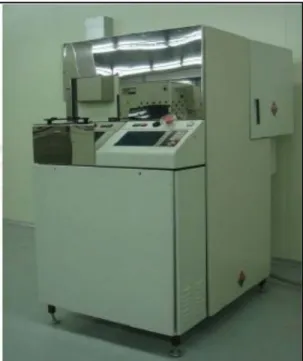
The Gasonics Aura 3010 machine is used by Analog Devices Inc.’s Wilmington, MA fabrication center for photoresist ashing and cleaning of semiconductor wafers by creating a low-pressure and low-temperature glow discharge, which chemically reacts with the surface of the wafer. The Aura 3010 system is composed of three main components [6]:
i. The reactor chamber which contains the system controller, the electro-luminescent display, the wafer handling robot, the microwave generator, and the gas box.
ii. The power enclosure wall box. iii. The vacuum pump.
Figure 1-4 shows a picture of the Gasonics Aura 3010 machine.
Figure 1-4: Gasonics Aura 3010 machine [7].
The machine is equipped with a wafer-handling robot that picks up a single wafer from a 25-wafer cassette and places it into the photoresist stripping process chamber. After a particular recipe is executed, the robot removes the wafer and places it on a cooling station if required before returning the wafer back to its slot in the cassette [6]. Inside the process chamber, the wafer rests on three sapphire rods and a closed loop temperature control (CLTC) probe. CLCTC is a thermocouple that measures the temperature of the wafer during the ashing process. Twelve chamber cartridges
embedded in the chamber wall then heat the process chamber. During the plasma ashing process, eight halogen lamps heat the wafer to the required process temperature. The process gases (oxygen, nitrogen, or forming gas) are mixed and delivered to a quartz plasma tube in the waveguide assembly where microwave energy generated by a magnetron ionize the gases into the monoatomic reactive species. The machine is
contact with the wafer surface as higher energy radicals can damage the wafer [6]. After the wafer has been stripped, the halogen lamps, microwave power, and the process gas flows are turned off and the process chamber is then purged with nitrogen before being vented to the atmosphere for wafer removal. The door to the process chamber is then opened and the robot removes the wafer to either place it on the cooling station or put it back in the cassette slot.
Analog Devices Inc.’s Wilmington, MA fabrication center has seven Gasonics Aura 3010 machines which have a codename of GX3000 where X is a number between 1 and 7. The experiments and analysis that are presented in this work were conducted on the G53000 machine.
1.3.2 Partial and Forming Recipes
A recipe can be defined as a set of input settings that can be adjusted on a tool or machine to execute a desired manufacturing process. For example, Figure 1-5 shows a sample recipe on the display screen of the Gasonics Aura 3010 machine.
The machine allows the operator to vary the quantities under the column “PARAMETER”. The process engineers in the company are responsible for proposing and executing an optimal recipe taking into account product quality, throughput and cost constraints. In addition to designing recipes for production wafers, Analog also designs recipes to run qualification tests. Qualification tests are used to periodically monitor product quality and verify machine calibrations. In this thesis, two qualification test recipes are studied. They are named “Partial” and “Forming”. The details of these two recipes are as follows:
i.
Partial: The Partial recipe is used for a qualification test to calibrate the rate of photoresist removal on a Gasonics Aura 3010 machine. The recipe is designed such that the photoresist mask is not completely removed from the wafer after the process. This is intentionally done so that the amount of photoresist removed and the time taken to do so can be recorded. An ideal Gasonics Aura 3010 machine would remove 6000 Angstroms of resist in eight seconds. The entire process with the Partial recipe takesapproximately 63 seconds with the first 20 seconds being allocated to heating the wafer to the necessary conditions and bringing the machine to steady state, the next eight seconds being allocated to the stripping process and the last 35 seconds being allocated to cooling the wafer. Table 1-1 shows the necessary machine parameters needed for the Partial recipe.
ii.
Forming: The Forming recipe is also a qualification test used to verify the rate of photoresist removal on the Gasonics Aura 3010 machine, but this recipe simulates the machine conditions in a different production recipe which is known as the “Implant” ash. The Implant recipe is used to strip photoresist from a production wafer that has undergone harsh treatments like ion implantation. The necessity to use a different recipe for wafers that have undergone harsh treatments comes from the fact that the chemistry of the photoresist mask may have changed during those treatments, and not accounting for these changes can damage the wafer and product. As in the case of the Forming recipe, the ideal machine will remove 6000 Angstroms but the time taken to do so in this recipe is 60 seconds. The entire process with the forming recipe takes approximately 115 seconds with the first 20 seconds being allocated to heating the wafer to the necessary conditions and bringing the machine to steady state (Step-1), the next 60 seconds to the stripping process (Step-2) and the last 35 seconds to cooling the wafer. Table 1-2 shows the necessary machine parameters needed for the forming recipe.Table 1-2: Machine parameters for the Forming recipe.
1.3.3 Data Collection and Logging
The key parameter that needs to be measured in the plasma ashing process is the amount of photoresist removed from the wafer after the process has been completed. The amount of photoresist removed divided by the time the Gasonics Aura 3010 tool was set to function gives the photoresist removal rate. Analog uses this parameter to monitor
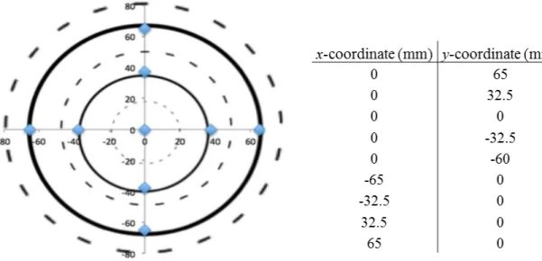
machine health. The tool used to measure the amount of photoresist is the Nanospec 9200. The Nanospec 9200 tool has the capability to accurately measure wafer thicknesses in the Angstrom range. The Nanospec 9200 tool is programmed to measure nine sites on each wafer. Figure 1-6shows the spatial distribution as well as the coordinate
measurements of the nine sites on each wafer. In the spatial distribution diagram, the blue dots indicate the sites where the measurements are taken.
Figure 1-6: Spatial distribution and coordinate positions of the nine sites.
The measurement procedure of the thickness of the photoresist in each of the nine sites is as follows:
i) The thickness of the photoresist is measured and recorded before the wafer undergoes the plasma ashing process. These are known as
“pre-measurements”.
ii) The thickness of the photoresist is measured and recorded after the wafer undergoes the plasma ashing process. These are known as
“post-measurements”.
iii) The difference between the pre-measurements and post-measurements gives the amount of photoresist removed during the process.
iv) The amount of photoresist removed can be divided by the duration of the plasma ashing process to give the resist-removal rate, which is included as an input and monitored by the Gasonics A3010 tool.
The amount of photoresist removed for each of the nine sites on a single wafer is recorded in an excel spreadsheet on which further analysis can be conducted. An example of the spreadsheet can be seen in Figure 1-7. In Figure 1-7, the columns in the
spreadsheet represent the measurements taken on the nine sites within a single wafer while the rows represent the different wafers measured. The Nanospec 9200 tool also logs the date and time of the measurement, which is very useful in detecting output anomalies.
Figure 1-7: Data logging from Nanospec 9200.
1.3.4 Calculation of Basic Statistics
The raw data collected from the Nanospec 9200 tool, as shown in Figure 1-7, needs to be processed in order to make meaningful implications of the underlying trends and patterns. This section introduces the method that was used to calculate three
statistical quantities:
i. The weighted average thickness of the nine sites on a single wafer (𝑥∗)
ii. The area-weighted standard deviation of the nine sites on a wafer (𝑠) iii. The within wafer non-uniformity parameter (WIWNU)
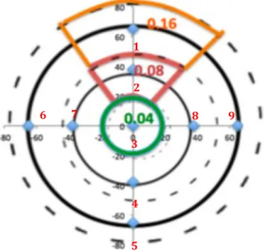
The nine sites that the Nanospec 9200 tool measures on a single wafer are distributed in a radial pattern from the center as can be seen in the spatial distribution diagram in Figure 1-6. Davis et al. has shown that in a radial distribution pattern, the calculation of any statistics on the sites measured on a wafer should take into account the
wafer area represented by each site for accurate analysis [8]. Figure 1-8shows the wafer areal representation of each site on a nine-site radial distribution pattern. The wafers used for the purposes of this study have a diameter of 80 mm or 6 inches.
Figure 1-8: Areal representation of each site on a wafer.
In Figure 1-8, site 3 represents the area bounded by the green circle (4% of the total wafer area), sites 2, 4, 7, and 8 each represent the area bounded by the red segments (32% of the total wafer area), and sites 1, 6, 5, and 9 each represent the area bounded by the orange segments (64% of the total wafer area).
The mean (𝑥∗) taking into account the areal representation of each site is
calculated as follows [9]:
𝑥∗ = '&()𝑤&𝑥&
𝑤&
' &()
(1.1) where 𝑥& is the wafer thickness measured at each site, 𝑤& is the weighted area associated with that site and 𝑁 is the number of sites.
1 2 5 4 6 7 8 9 3
The weighted standard deviation taking into account the areal representation of each site can be derived as follows starting from the fundamental standard deviation formula:
𝑠+,+-./&012/3 = '&() 𝑥&− 𝑥 5 𝑁 − 1
(1.2) The unbiased estimate for the area-weighted standard deviation, replacing 𝑥 with the weighted mean 𝑥∗, can be written as:
𝑠 = '&()𝑤& 𝑤&
'
&() 5− '&()𝑤&5
∙ 𝑤& 𝑥& − 𝑥∗ 5 '
&()
(1.3) In both equations, 𝑥& is the wafer thickness measured at each site, 𝑤& is the weight
associated with that individual site, and 𝑥∗ is the weighted average mean. The derivation
for Eq. (1.3) can be found in one of NASA’s Giovanni documents [9].
The within-wafer non-uniformity parameter (WIWNU) taking into account the areal representation of each site is calculated as follows:
𝑊𝐼𝑊𝑁𝑈 = 𝑠 𝑥∗
(1.4) where 𝑠 is the weighted standard deviation and 𝑥∗is the weighted average mean [8].
1.4 Problem Statement
This section outlines the motivation behind the work done alongside this thesis with Analog Devices, Inc. to improve yields and increase throughput of the plasma ashing process. As manufactured semiconductors are shrinking in various dimensions, more sophisticated control systems need to be implemented to achieve higher yields. Analog is also adapting to these changes by implementing Internet of Things (IoT) and
Advanced Control Systems. From observing Analog’s IoT pilot project, it is clear that the already-existing control system does not facilitate steps to keep the process in control, and the machines operate at different values of the critical dimensions measured for the process. ADI stated that such differences that might result in yield losses appear later at the end-of-the-line after many process steps. Such losses can become more problematic in high-resolution manufacturing and for more expensive large-scale processes.
Therefore, the work outlined in this thesis including an improvement plan for the use of statistical control, process modeling and eventually machine matching, would be a
critical step towards the implementation of Advanced Control Systems such as Predictive Maintenance (PM).
1.5 Outline of Thesis
This chapter has just discussed the background information of Analog Devices as well as the dry etch process and data collecting conventions around which this thesis revolves. Chapter 2 outlines the fundamental SPC procedures and details, with equations and examples, the mathematical tools that are relevant to making recommendations to the company. Chapter 3 discusses the SPC methodology and how it will be applied to the nine-month resist-thickness data from the fabrication facility. Chapter 4 will then delve into these analyses in a quantitative manner. Control charts and correlation graphs will be presented accordingly. Chapter 5 will consolidate the results, presenting a solution on how to proceed and evaluate the potential benefits of adopting the solution. Finally, the last chapter (Chapter 6) will draw a conclusion from the statistical analyses done in prior chapters. Suggestions for further studies will also be discussed in the final section.
Chapter 2: Theoretical Review of Key Concepts
This chapter will introduce the mathematical concepts and models that are
relevant to the construction of this thesis. This includes both theoretical SPC background from textbooks by May and Spanos and Montgomery as well as prior research that has applied those concepts in both academic and industrial settings [5, 10].
2.1 Statistical Process Control (SPC)
Statistical Process Control or SPC is an applied statistics concept used to monitor and control the quality of a manufacturing process by minimizing process variability. With decreased variability, the rate at which defective parts occur also decreases, thereby reducing waste. Key topics that are applied towards the collaboration with Analog
Devices include Shewhart control charts, analysis of variance (ANOVA), design of experiments (DOE) and hypothesis-testing.
2.1.1 Origin of SPC
The SPC method was introduced by Walter A. Shewhart at Bell Laboratories in the early 1920s. Later in 1924, Shewhart developed the control chart and coined the concept of “a state of statistical control” which can actually be derived from the concept of exchangeability developed by logician William Ernest Johnson in the same year in one of his works, called Logic, Part III: The Logical Foundations of Science [11]. The theory was first put in use in 1934 at the Picatinny Arsenal, an American military research and manufacturing facility located in New Jersey. After seeing that it was applied
successfully, the US military further enforced statistical process control methods among its other divisions and contractors during the outbreak of the Second World War. [12]
2.1.2 Shewhart Control Charts
A Shewhart control chart essentially plots an output parameter or some indicator of the process performance over a measure of time [13]. These plots are then bounded by control limits which are, as a rule-of-thumb, three standard deviations away from the mean on either side. An example of a control chart is shown in Figure 2-1 [14].
Figure 2-1: Example of a Shewhart control chart.
Points marked with X’s are points that would be rejected based on Western Electric Rules (set of rules that indicate when process is out of control). Control charts can either be plotted as a run chart or an x-bar chart. The run chart plots each measurement separately on the chart while the x-bar control chart plots the average of several measurements. Because the thickness measurements associated with the plasma ashing process do not come in batches and are sampled individually over periods of time, only the run chart will be relevant in subsequent analyses here.
The goal of plotting control charts is to monitor the manufacturing process and detect when it is out of control. Assuming that the data plotted is normally distributed, which is usually the case for most processes, the chance that any single point would lie above the upper control limit UCL or below the lower control limit LCL (in the case of the typically used three standard deviations above or below the mean) would be less than 0.3% [14]. Assuming that a set of data is normally distributed with mean µ and variance σ 2, the UCL and LCL can be expressed as:
𝑈𝐶𝐿 = 𝜇 + 3𝜎 𝐿𝐶𝐿 = 𝜇 − 3𝜎
(2.1) With that, the probability of a point lying beyond the limits for any normally distributed data set can be solved for:
𝑃 𝑋 < 𝑈𝐶𝐿 = 𝑃 𝑍 <𝜇 − 𝐿𝐶𝐿
𝜎 = 𝑃 𝑍 < 3 ≅ 0.0013
𝑃(𝑋 > 𝑈𝐶𝐿| 𝑋 < 𝐿𝐶𝐿 = 𝑃 𝑋 > 𝑈𝐶𝐿 + 𝑃 𝑋 < 𝐿𝐶𝐿 = 0.0013 + 0.0013 𝑃(𝑝𝑜𝑖𝑛𝑡 𝑙𝑖𝑒𝑠 𝑜𝑢𝑡𝑠𝑖𝑑𝑒 𝑐𝑜𝑛𝑡𝑟𝑜𝑙 𝑙𝑖𝑚𝑖𝑡) ~ 3%
(2.2) Besides the upper and lower control limit rule, there are other Western Electric Rules that could be used as guidelines to suspect when the process is out of control. These include 1) if two out of three consecutive points lie either two standard deviations above or below the mean 2) four out of five consecutive points lie either a standard deviation above or below the mean 3) nine consecutive points fall on the same side of the centerline/mean [14].
2.2 Analysis of Variance
Analysis of variance or ANOVA is a collection of statistical models used to analyze the differences among group means and variances between and within sets of data. This would thus indicate the difference in the process associated with those data. ANOVA only came into substantial use in the 20th century, although mathematicians have been passively implementing parts of it in prior academic work, the earliest of which dates back to when Laplace conducted hypothesis-testing in the 1770’s [15].
In semiconductor processing, extra attention will be paid to the nested analysis of variance. This is the analysis that is done when data can be broken down into groups, subgroups and etc. Nested variance analysis will determine the significance of the variance between and within groups and subgroups of data [16]. For instance, say there are W groups of data with M data in each of those groups; the mean squared sum between groups (MSW) and within groups (MSE) can be calculated as follows [5].
𝑀𝑆] = 𝑆𝑆] 𝑊 − 1 (2.3) 𝑀𝑆^ = 𝑆𝑆^ 𝑊 𝑀 − 1 (2.4)
where:
𝑆𝑆] = 𝑠𝑞𝑢𝑎𝑟𝑒𝑑 𝑠𝑢𝑚 𝑜𝑓 𝑑𝑒𝑣𝑖𝑎𝑡𝑖𝑜𝑛𝑠 𝑜𝑓 𝑔𝑟𝑜𝑢𝑝 𝑚𝑒𝑎𝑛𝑠 𝑓𝑟𝑜𝑚 𝑔𝑟𝑎𝑛𝑑 𝑚𝑒𝑎𝑛 𝑆𝑆^ = 𝑠𝑞𝑢𝑎𝑟𝑒𝑑 𝑠𝑢𝑚 𝑜𝑓 𝑑𝑒𝑣𝑖𝑎𝑡𝑖𝑜𝑛𝑠 𝑜𝑓 𝑒𝑎𝑐ℎ 𝑑𝑎𝑡𝑎𝑝𝑜𝑖𝑛𝑡 𝑓𝑟𝑜𝑚 𝑖𝑡𝑠 𝑔𝑟𝑜𝑢𝑝 𝑚𝑒𝑎𝑛
Note that 𝑆𝑆] sums up the grand-group mean deviation for every individual point. So in this case, each squared difference between grand and group mean is multiplied by M before summing them together. The significance of the between-group variation could then be determined, given that the ratio 𝑀𝑆]/𝑀𝑆^ approximately follows the F-distribution.
It is important to take into account that the observed variance of the group averages does not reflect the actual wafer-to-wafer variance because of the existence of sub-variation (group variance). The observed variation between the group averages 𝜎.5
can be written as a linear combination of the true variance 𝜎.5 and the group variance 𝜎 f5 [5]. 𝜎.5 = 𝜎 .5 + 𝜎f5 𝑀 (2.5) Hence the true group-to-group variance can be expressed as:
𝜎.5 = 𝜎 .5 −
𝜎f5
𝑀
(2.6) From this, both the group-to-group component and the within-group component can be expressed as a percentage of the total variance. This variance decomposition enables one to differentiate between measurements among and within silicon wafers.
2.3 Design of Experiments
Design of experiments (DOE) is a systematic method to determine how factors affecting or the inputs to a process quantitatively relate to that process’s output. It is a
information could then be used to tune the process inputs in order to optimize the outputs of that process to achieve production goals. The focus of DOE is not on figuring out how to perform individual experiments but rather on planning the series of experiments in order to obtain the most information in the most efficient manner. This leads to the concept of designing fractional factorial experiments.
Factorial experiments allow for both individual factor and multiple-order
interactions (effect of varying multiple factors simultaneously) to be evaluated from one set of experiments. Single factor relationships are also termed “main effects.”
Experimental design is built upon the foundation of analysis of variance and
orthogonality. Analysis of variance is used to break down the observed variance into different components while orthogonality is, in other words, the relative independence of multiple variables which is vital to deciding which parameters can be simultaneously varied to get the same information [10]. For this work, experiments were done based on pre-designed half-factorial experiments and it would extort from the main objectives of this project to stress all the theoretical background that led up to the designs.
As reducing from full-factorial to half-factorial experimental designs requires fewer experimental combinations at the expense of aliasing or confounding main effects with multiple-order interactions. These interactions, effects of which are assumed negligible, usually include some second degree interactions and third degree (or higher) order interactions that are typically less significant than lower-degree interactions. For example, Table 2-1 shows the full factorial (23) experimental design for a two-level test with three variable input parameters (A, B and C) as the main effects. “-1” indicates a low setting while “+1” represents the high setting of the input parameter. The two levels mean that each main effect will only be varied between two values, the high value and the low value. [10]
A B AB C AC BC ABC (1) -1 -1 +1 -1 +1 +1 -1 a +1 -1 -1 -1 -1 +1 +1 b -1 +1 -1 -1 +1 -1 +1 ab +1 +1 +1 -1 -1 -1 -1 c -1 -1 +1 +1 -1 -1 +1 ac +1 -1 -1 +1 +1 -1 -1 bc -1 +1 -1 +1 -1 +1 -1 abc +1 +1 +1 +1 +1 +1 +1
Table 2-1: 23 full factorial experimental design.
By defining the following identity relation and aliases: I = ABC
A + BC B + AC C + AB,
a half factorial experimental design can be made. Table 2-2 shows the half factorial design. This is extremely powerful when there are several factors to consider as it can immensely reduce the number of experiments needed.
Run Factors A B C 1 -1 -1 +1 2 +1 -1 -1 3 -1 +1 -1 4 +1 +1 +1
2.4 Hypothesis-Testing
A statistical hypothesis test compares at least two sets of data that can be modeled by known distributions. Then assuming that those data follow the proposed distributions, the probability that a particular statistic calculated from the data occurs in a given range can be calculated. This probability is also referred to as the p-value of a test and is ultimately the basis to either accept or reject the current state or the null hypothesis. The acceptance/rejection cutoff is marked by a rather arbitrary “significance level.”
Generally, the decision as to what significance level to use would depend on the consequences of either rejecting a true null hypothesis (type I error) versus accepting a false null hypothesis (type II error). The three upcoming sections will outline the three tests around which this project revolves. Each of these tests centers on a different distribution. [13]
2.4.1 Z-Test for Detecting Mean-shifts
The Z-test technically refers to any hypothesis test whereby the distribution of the test statistic under the null hypothesis is modeled by the normal distribution. This
becomes useful because of the central limit theorem. With the central limit theorem, means of a large number of samples of independent random variables approximately follow a normal distribution. Mathematically, the sample mean of any distribution of mean 𝜇 of sample size n and standard deviation 𝜎 would be normally distributed with the same mean and standard deviation g
+ , or ~𝑁 𝜇, g
+ . [13]
For instance, when testing for whether the mean of a given process (with default mean µ and standard deviation σ) has shifted, the following hypotheses can be formed [10].
𝐻j: 𝜇 = 𝜇j 𝐻): 𝜇 ≠ 𝜇j
(2.7) The null hypothesis H0 is assumed to hold with the true mean µ being equal to the
assumed mean µ0 to begin with. Now given a set of data or observations with sample mean 𝑥 > 𝜇j, the test statistic Z0 could be calculated.
𝑍j =
𝑥 − 𝜇j 𝜎/ 𝑛
(2.8) The p-value can then be deduced as follows.
𝑝-value = 𝑃 𝑥 > 𝜇j = 𝑃 𝑧 > 𝑍j
(2.9) Given a significance level α, the null hypothesis would be rejected if p-value < α/2 or, equivalently, if Z0 > Zα/2, then the alternative hypothesis H1 would be accepted, that the
mean has shifted.
The probability of encountering a type I error would be the significance level α itself, i.e., P(Type I Error) = α. Given an alternative mean 𝜇), the distribution of the alternative hypothesis could be written as 𝑥~𝑁 𝜇), 𝜎/ 𝑛 . Hence the probability of making a type II error could be calculated:
𝑃 𝑇𝑦𝑝𝑒 𝐼𝐼 𝐸𝑟𝑟𝑜𝑟 = 𝑃 𝑥 < 𝑥wx&2&wyz
(2.10) where 𝑥wx&2&wyz is the 𝑥 that corresponds to Z1-α/2 under the old mean 𝜇j.
𝑥wx&2&wyz = 𝜇j+ 𝑍)-{ 5 ∙ 𝜎
(2.11) Therefore, continuing from Eq. (2.11)
𝑃 𝑇𝑦𝑝𝑒 𝐼𝐼 𝐸𝑟𝑟𝑜𝑟 = 𝑃 𝑍 < 𝜇j− 𝜇)
𝜎 + 𝑍)-{5
(2.12) As previously mentioned, the significance level would depend on the tolerance for these two errors. For instance, if the detection of a mean shift triggers a very costly alarm, then a lower α would be desired in order to minimize P(Type I Error) or practically the probability of a false alarm. However, if it is very crucial to detect the mean shift even at
the cost of incurring several false alarms, then a higher α would be desirable to minimize P(Type II Error).
Note that the example presented is a two-sided test because the p-value is tested against the probability of the sample mean being too far from the mean on either side. If it was a one-sided test, with the alternative hypothesis would be 𝐻): 𝜇 > 𝜇j or 𝐻): 𝜇 < 𝜇j, the p-value would be compared to α and the null hypothesis would be rejected if Z0 > Zα (no ½ factor on α). The format of other tests will more or less follow the same
structure as the example above but with different formulas for calculating the test statistics and their probabilities.
2.4.2 F-test
Rather than detecting a mean shift, the F-test indicates whether the ratio of the variances of two sets of data is statistically significant. Following the same method as in the previous Z-test example, the F-test begins with formulating hypotheses around the variances (s12 and s22) of two sets of data [13].
𝐻j: 𝑠)5 = 𝑠55
𝐻): 𝑠)5 ≠ 𝑠55
(2.13) The test statistic F0 in this case is simply the ratio of the variances where the numerator is the greater of the two variances, s12 > s22. F0 can approximately be modeled by the F-distribution.
𝐹j = 𝑠)5 𝑠55
(2.14) With that, the null hypothesis H0 would be rejected under a certain significance level α if 𝐹j > 𝐹+}-),+~-),{ where n1 and n2 represent the sample sizes of the first and second data sets respectively. Alternatively, the p-value could be calculated and tested directly against the significance level. The calculation of the p-value is shown in Eq. (2.15).
𝑝-value = 𝑃 𝐹 > 𝐹j
(2.15) This is a one-sided test as can be seen intuitively. To modify this into a two-tailed test, F0 would simply be compared with 𝐹+}-),+~-),{/5, where n1 and s1 represent the first data set (i.e., s12 is not necessarily larger than s22). Typically for testing whether or not two variances are different, a two-tailed test would not be used.
2.4.3 Bartlett’s Test
Bartlett’s test is used to determine whether k sets of numbers of were sampled from distributions with equal variances. The null and alternative hypotheses can be formulated as follows:
𝐻j: 𝑠)5 = 𝑠
55 = 𝑠•5… = 𝑠•5
𝐻): 𝑠&5 ≠ 𝑠
‚5 for at least one pair (i, j)
(2.16) Given the k samples with sample sizes ni, and sample variances si2, the test statistic T can
be written as follows [17]. 𝑇 = 𝑁 − 𝑘 ln 𝑠…5 − 𝑛&− 1 • &() ln 𝑠&5 1 +3 𝑘 − 11 𝑛 1 &− 1 − 1 𝑁 − 𝑘 • &() (2.17) where N is the total number of data points combined and sp2 is the pooled estimated
variance. 𝑁 = • 𝑛& &() (2.18) 𝑠…5 = 1 𝑁 − 𝑘 𝑛&− 1 𝑠&5 • &
T can be approximated by the chi-squared distribution. H0 would therefore be rejected under a significance level α if 𝑇 > 𝜒•-),{5 . [17]
Chapter 3: Statistical Process Control Methodology
This chapter discusses the data analysis procedure used to support the statistical process control methodology. Based on the background SPC theories and literature reviews presented in Chapters 1 and 2, a plan was developed to first make sense of the data that comes out of the Gasonics tool and then to use that information to make valuable conclusions that will lead to improving the performance of the machine.
3.1 Source of Data
Data is obtained from the Gasonics A3010 machines at Analog’s facility in Wilmington. For simplicity and to isolate our investigation to as few external variables as possible, SPC analysis is limited only to the data from the Partial recipe from the G53000 machine. This was the etching process that was responsible for monitoring the removal rate by only partly removing coated resist from silicon wafers. The data extracted consists of the thickness of the photoresist layer before and after the etching process. The
difference between the two numbers is the amount (in thickness) of photoresist removed. Dividing this thickness by the time spent etching is a measure of resist-removal rate (typically in Å/min). Each wafer undergoes this measurement at nine sites. The average of resist-removal rate on the nine sites is then used to plot the control charts.
The data analyzed in this thesis is extracted from the end of August 2015 all the way through to the middle of March 2016. The measurements were taken approximately once every two days. The general procedure begins by applying some of the simplest methods such as the traditional run-chart, which then inspires bringing in more
complicated analytical techniques to make sense of the data which will be discussed in subsequent sections in this chapter.
3.2 Tests for Normality
Before any of the conventional SPC theories can be applied, the first step is always to test the data for normality. To evaluate data distribution for normality, either a histogram or a normal probability plot could be used. In a histogram, one observes how close the distribution of the data is to the “bell-curve” shape that would be seen if the data
linearly the sorted data fits to the selected values. The concept of a normal probability is derived from what is called the quantile-quantile plot (or Q-Q plot) that graphs the quantiles of two distributions against each other [10].
A histogram of the data (for G53000) is shown in Figure 3-1. This is the average of the nine sites in each wafer. Histograms for the nine individual sites also exhibit similar bell-shaped trends. This supports the assumption that the output thickness could approximately be modeled by a normal distribution.
Figure 3-1: Histogram of the nine-site average thickness from G53000.
Figure 3-2 is a normal probability plot of the same data shown in the previous histogram in Figure 3-1. The bulk of the data on the plot lies very closely to the linear fit, hence also supporting the assumption of a normal approximation on the distribution of the output thickness. Note that it is expected for the data on both ends of the distribution to deviate farther from the fit than those nearer to the mean. This is why there is more deviation from the linear fit for the thicknesses less than 5700 Å and greater than 7000 Å as seen in the plot shown in Figure 3-2.
Figure 3-2: Normal probability plot of nine-site average from G53000.
3.3 Fundamental Analysis Procedure
Comparing the control limits on Analog’s current run charts to the three sigma (±3σ) limits shows that the three sigma limits are slightly tighter than those on ADI’s current SPC run charts. Shewhart x-bar and s-charts were also plotted, assuming that the each of the nine-site measurements were independent replicates (i.e., plotted x-bar and s-charts with n = 9). From the control s-charts, a few outliers that were outside of the control limits could be seen. These were later found to be erroneous data and were removed from the analysis. These charts, however, appeared to produce overly tight control limits. From this observation, the team chose to respectively explore 1) the difference between the variation within wafer (spatial variation) and between wafers (temporal variation), and 2) the correlation between the nine-site measurements.
The analysis of nested variance was initially used to separate the components of variation from one measurement to the next and, more specifically, to determine whether the variation between measurements or wafers was even significant at all. Results from this provided motivation to further look into the correlation between the nine sites. The concept of principal component analysis was used to relate the measurements on these nine sites. Throughout this process, it was noted that the correlation and variation between the 9 sites can largely be explained by a simplified factor, namely the non-uniformity element. Finally, the run charts were re-plotted using the parameters and factors deduced from those analyses. This would allow for those charts to be juxtaposed against the traditional SPC method. Each of these steps is presented in further detail in Chapter 4.
Chapter 4: Control Charts: Analysis
This chapter incorporates all of the data analyses done on the nine months of data in a coherent order. The purpose is to take readers step-by-step through the logic of how and why certain tests and analyses were done subsequent to the results summarized in Chapter 3.
4.1 Raw Shewhart Charts
One of Analog’s major issues is they are not able to detect as many of the
problematic data points as they would like to and as early as they would hope to. And so maintenance would not occur at optimal times. The first milestone is therefore to refine these control charts in such a way that would allow ADI to effectively detect problems with the Gasonics tool in advance of when it would inflict further harm on its operations.
The Shewhart charts that were plotted assuming each of the nine sites to be independent replicates generated no out-of-control points as will be seen in Section 4.1.2 on the x-bar chart in Figure 4-2.
4.1.1 Analog’s Original Run Charts
Analog’s original control limits for the plasma ashing process were calculated collectively for all of the machines with the means of the resist removed on all machines pooled together. The population standard deviation of the data was estimated to be half of the range of those means. And it follows that the upper and lower control limits were three times that (estimated) standard deviation above and below the mean. With this method, the control limits on all of the machines would be identical. The original run chart with control limits for machine G53000 is shown in Figure 4-1. As seen, the current control limits allow for practically every out-of-control state to go undetected. Note also that the ADI’s original control charts plot the non-weighted average of the thicknesses removed on each wafer.
Figure 4-1: Original control chart on G53000.
Analog Devices considers data points to be out of control points and would require machine shut down and component inspection in either of the following two cases:
i. Any data point that crosses the 3-sigma control limit
ii. Two or more consecutive data points crossing the 2-sigma control limit
4.1.2 Three Sigma Shewhart Control Charts
On the other hand, contrary to ADI’s original run charts, the control limits
calculated using the traditional Shewhart x-bar chart seems to be too tight for the process and it would not make sense financially for ADI to shut down and maintain the machine as frequently as indicated by the x-bar chart. Note the x-bar chart also does not take into account the areal weighting of the within-wafer measurements. The control limits on the traditional x-bar chart were calculated as follows [13]:
i. The mean of the nine sites on each wafer and the within-wafer standard deviation of the nine sites were calculated:
4500 5000 5500 6000 6500 7000 0 20 40 60 80 100 120 Th ic k n es s (Å ) Sample Number
𝜇& = 𝑥‚ ‚(‡ ‚() 9 , 𝑠& = 1 8∗ (𝑥‚− 𝜇&)5 (4.1) ii. The mean of the within-wafer standard deviations or s-bar was then calculated as
follows:
𝑠 = ( 𝑠&)/𝑚
(4.2) where m is the total number of wafer runs.
iii. The 3-sigma control limits for the 𝑥-chart can then be written out as: 𝑈𝐶𝐿 = 𝑥 + 3𝑠
𝑐Š 𝐿𝐶𝐿 = 𝑥 − 3𝑠 𝑐Š
(4.3) where 𝑐Š is a constant used to estimate the standard deviation of the process and 𝑥 is the grand mean (𝑐Š = 0.9693 for n = 9). The Shewhart x-bar control chart is shown in Figure 4-2. As seen, almost a third of the points lie beyond the UCL and LCL. On further
investigation on the comments recorded by the operators of the machine, it was noted that many of these out-of-control points, including those that are circled in green in the graph shown in Figure 4-2, would have merely been false alarms as the machine seemed to be operating as expected and the wafers were well within the specification limits. After discussing with the manufacturing team, it was determined that the control limits generated using this method are now overly tight and that this method would not be feasible for ADI to implement.
Figure 4-2: Shewhart x-bar control chart with control limits calculated using the average nine-site standard deviation as 𝑠.
To construct the x-bar chart, the average of the within-wafer standard deviation was used as 𝑠 for calculating the control limits. This would usually be done when the measurements on the nine sites are uncorrelated and with the assumption that the
measurements of all the sites on all wafers come from the same overarching distribution. One hypothesis as to why the control limits on the x-bar chart were not an accurate representation of the state of the process was that the resist removal rate on the nine sites within a single wafer were not independent; some (if not all) sites may have been
strongly correlated with each other.
4.1.3 Principle Component Analysis
A preliminary test for this correlation hypothesis was to make a scatter plot of the data from any two sites and look for trends. The scatter plot of site 2 vs. site 3, as shown in Figure 4-3, clearly shows a strong correlation pattern and preliminarily validates the hypothesis that the two sites are indeed correlated. The linear fit has a slope of very close to one, and the data on the plot lies very closely to the linear fit. The R-squared value is also very close to one, indicating a high quality of fit. One might even be able to infer this
5200 5400 5600 5800 6000 6200 0 20 40 60 80 100 120 140 Th ic k n es s (Å ) Sample Number
as an indication that sites 2 and 3 are not that much statistically different from each other, though that is not as relevant at this stage.
A more formal approach to test for redundancies in the nine-site data is to analyze the variation of the data set along its principle components. This method is known as principle component analysis. The principle components are a set of orthonormal axes that capture the maximum variation in each dimension of the data set. If the variation of the data set is equally distributed across all the principle components, then the entire data set is uncorrelated. If most of the variation is captured by only some of the principle components, then those principle components that capture the least variation are redundant and the number of dimensions or variables can be reduced.
Figure 4-3: Data from site 2 plotted against data from site 3.
To perform a principle component analysis on the nine-site data set, an m x n matrix X was formulated where m is the total number of wafers and n is the number of measurements on each wafer. The covariance matrix (C) of X was then calculated as follows [18]:
y = 1.09x - 445.61
R² = 0.95
5000 5500 6000 6500 5000 5500 6000 6500 Si te 2 Site 3𝐂 =1 n𝐗𝐗′
(4.4) The principle components of the nine-site data set are the eigenvectors associated with the covariance matrix C and the variance across each principle component is the
eigenvalue associated with that principle component/eigenvector. This data set will have nine principle components, as there are nine measurement sites on each wafer. These values were computed in MATLAB. The percentage of variation captured by each principle component is shown in Table 4-1 and can be calculated using the following formula: %𝑉𝑎𝑟𝑖𝑎𝑛𝑐𝑒 = 𝜆& 𝜆& &(‡ &() ∗ 100 (4.5) where 𝜆& is the eigenvalue associated with the principle component i [18].
%Variance Captured by Each Principle Component
91.242 4.260 1.967 1.314 0.995 0.096 0.055 0.052 0.020
4.2 Separation of Variation Components
It is apparent from the nature of the etching process data and the control charts that there has to be a differentiation between the spatial (within-wafer) variance and the temporal (between-wafer) variance. Therefore, ANOVA was performed, results of which are shown in Tables 4-2 and 4-3. The MS ratio (between-wafers to within-wafer or MSGROUP/MSERROR) or F-value was found to be 6.54. This translates into a p-value on the order of 10-68 which is way below any reasonable significance level. Hence it can be concluded with virtually full confidence that the variation between each wafer run is significant to the process. Note that the reverse conclusion could not be drawn with this method without affirming that there is no spatial correlation within each wafer.
Table 4-2: Process variance broken down into the within-wafer or “error” component and the between-wafer or “group” component.
The total variation of the etching process was further separated into their components. This was done by analyzing the nested variance in the data. The results of the calculation are shown in Table 4-2. SS and MS values are calculated using formulas presented in Eq. (2.3) through Eq. (2.6) in Chapter 2. The spatial variation accounted for 62% of the total variation while the temporal variation accounted for only 38% of the total variation. In other words, more than half of the variation associated with this process can be explained by the within-wafer variation. However, because of the observable trends in the temporal run charts and the fact that the ANOVA F-test indicated an exceedingly high significance level, there is reason to suspect that a large part of the spatial variation could be owed to strong correlations between the nine sites.
VARIANCE COMPONENTS
ERROR (site to site) 38253 1 38253 38253 61.89
GROUP (wafer to wafer) 250256 9 27806 23556 38.11
TOTAL 288509 1 288509 61809 # data in SS Observed Variance Estimated Variance % Est Variance MS Variation Source
Table 4-3: ANOVA table to test the significance of spatial variation.
4.3 Additional Modified Parameters to Monitor
The monitoring strategy proposed by the classical Shewhart control strategy using the nine-site sample standard deviation would not be feasible for Analog’s plasma ashing operation. Control limits would be too narrow and would constantly trigger unwanted alarms. On the other hand, with the original control chart method, the system would still not have detected problematic data points during the past nine months when there
definitely was a significant amount of improperly etched wafers. Analyzing the variation components and within-wafer correlation suggests that a wafer-to-wafer run chart might be most suited for Analog’s purpose.
The significance of the spatial variation indicates that it might also be beneficial to look into more parameters that would account for the within- versus between-wafer distribution of the output thickness. The next two sections will re-visit the concepts of weighted average thickness and within-wafer non-uniformity mentioned in the first two chapters, plotting them on control charts to see what other benefits could be realized.
4.3.1 Weighted Average Thickness
This section is partly a continuation from Section 1.3.4 of this thesis. The weighted average thickness (WAT) is calculated from Eq. (1.1) where the measurement of each site is roughly weighted according to the size of the area it represents. The control chart plotting the weighted average thickness (instead of non-weighted) is shown in Figure 4-4. The average nine-site standard deviation 𝑠 (weighted or not) would not be relevant in this case so a plain run chart of the individual weighted average values were plotted. Note that from this point forward, all data plotted on control charts will account for areal weighting. The central line or mean µWAT and sigma σWAT are the average and
SS DOF MS F-value P-Value (Pr>F) SSG (Temporal) 31282053 125 250256 6.54 6.09×10-69 SSE (Spatial) 38558931 1008 38253 SSD (Total) 69840984 1133 61643
standard deviation of all 127 runs of the WAT values. This is represented formulaically in Eq. (4.6) and (4.7) as follows.
𝜇]‘’ = 𝑊𝐴𝑇& )5” &() 127 (4.6) 𝜎]‘’ = )5”&() 𝑊𝐴𝑇&− 𝜇 127 − 1 (4.7) where in both cases, WATi represents each of the individual run values the weighted
average resist-thickness removed.
In this chart, the ±3σ control limits become wider than that in the Shewhart control chart of the non-weighted average thickness (Figure 4-2). The trends, however, are almost identical.
Figure 4-4: Weighted average thickness run chart. Grand mean and ±3σ calculated based on all 5000 5500 6000 6500 0 20 40 60 80 100 120 Th ic k n es s (Å ) Sample Number
Even though there are no points that lie outside the upper or lower control limit in this chart, it is clear that the process is not in control. Especially if the Western Electric rules were to be applied, it could be concluded that many or most of the runs plotted are not in control. Starting at sample 12, there is a clear drift downwards. Performing a formal pairwise Z-test to test for a mean shift between samples 1-27 and 37-63 (assuming the population variance is equal to the variance of the entire nine months of data), it can be concluded that the mean has shifted with a 1% significance level, with a Z-value of 7.18 which translates into a p-value of essentially zero. Referring to the logged
observation, the drift was due to an adjustment in the magnetron voltage that creates the microwave power. Shortly after, there was a leak found in the O-ring which may have worsened the tool’s condition.
Defining specific criteria to detect out-of-control output requires a more
elaborated discussion with ADI’s manufacturing team. Slight tweaks can be made on the control chart to make many out-of-control data points more apparent, though these techniques will involve cost-benefit tradeoffs to consider. These different options will be discussed in more depth in Chapter 5. In the meantime, there is another parameter that cannot be neglected when dealing with semiconductor manufacturing processes. This is the within-wafer non-uniformity.
4.3.2 Non-uniformity
Similar to the last section on weighted average thicknesses, this chapter also continues from Section 1.3.4. The within-wafer non-uniformity (WIWNU) is defined as the weighted coefficient of variation of the sites within a wafer. Monitoring the spatial uniformity is crucial to maintaining lean and high quality semiconductor manufacturing and will come in especially useful when trying to optimize for the most effective process parameters [19]. Process optimization of this same process can be read more about in the corresponding thesis written by Nerurkar [2]. Note that because of the areal adjustment concept, the mean of the nine sites will be the weighted average as per what was
explained in the previous section. The control chart of the WIWNU is plotted and shown in Figure 4-5. Again, the average nine-site standard deviation 𝑠 would not be relevant in this case so a plain run chart of the non-uniformities were plotted, now using the mean
µWIWNU and standard deviation σWIWNU calculated using the 125 individual wafer-level run values to define the center line and ±3σ limits.
𝜇]—]'˜ = 𝑊𝐴𝑇& )5” &() 127 (4.8) 𝜎]—]'˜ = )5”&() 𝑊𝐴𝑇&− 𝜇 127 − 1 (4.9)
Figure 4-5: WIWNU run chart.
There is a much different trend in the WIWNU run chart than in the WAT run chart. Just by inspection, it can be seen that WIWNU is more in-control than the thickness removed over the past nine months. However, there are some out-of-control points that would be detected in the WIWNU chart that otherwise would not have been detected with the WAT run chart alone, one of which is sample 89 (circled in Figure 4-5) which singly lies out of the upper and lower control limits. This run signifies the leak across the door of the Gasonics machine which was a result of the O-ring breakdown
0.00 0.01 0.02 0.03 0.04 0.05 0.06 0 20 40 60 80 100 120 Wi th in -W af er N on -U n if or m it y Sample Number
According to the respective logged comments, this was due to a power glitch, causing at least a temporary mean shift (there was no further data readily available to confirm whether or for how long this mean shift persisted). This problem is one that would not have been detected by the WAT run chart, even if all the Western Electric Rules were to be enforced. This underlines the importance of monitoring the WIWNU in addition to monitoring the weighted average removed resist thickness.
Chapter 5: Benefits for Analog Devices, Inc.
To evaluate the benefits of the statistical process control analyses done throughout this thesis, all the methods and options must be compared. Chapter 5 will focus on
consolidating the results obtained from Chapter 4. In addition, a few different cases of the previously presented analyses will be re-introduced to exemplify the associated costs and benefits. Specific recommendations will be proposed together with the possible tradeoffs that should be considered between each of the choices. Finally, this will lead to the conclusion of how Analog should consider its options on how to proceed from this point forward, as well as what further investigations could be conducted to make more
informed decisions.
5.1 Choosing “Control Groups”
To systematically implement the SPC methods that have been discussed in this thesis, the focus question is how one chooses the control group off of which to calculate the control limits. In other words, Analog needs to decide, based on its needs for
maintenance, how “in control” it wants this etching process to be. For instance, looking back at the run chart in Figure 4-4, Analog can conclude that the entire process is
sufficiently in control, assuming that all the observed fluctuation is just part of the natural variation of the entire system. This will be referred to as the “lumped data/trend” method. On the other hand, Analog can also be as strict as to take only a small group of points with the least variation, for instance samples 45 to 60, to be the control group, and determine that any points or group of points that lie out of the control limits calculated from that control group is out of control. This will be referred to as the “small-window control limits” method. In an ashing process, it is beneficial to detect control violations as early as possible to prevent compounded downstream effects [20]. Yet devoting too much attention to insignificant fluctuations can also result in unnecessary maintenance costs.
Cassidy showed that simulation models can be used to optimize control limits to achieve the desired optimal cost-saving decisions [21]. However, because precise
information on yield and maintenance benefits is not readily available, a more simplified approach is taken here. A few extreme cases and methods were examined on the nine
![Figure 1-2: Semiconductor processing steps [4].](https://thumb-eu.123doks.com/thumbv2/123doknet/14477479.523468/12.918.146.783.194.474/figure-semiconductor-processing-steps.webp)
![Figure 1-3: Ashing process schematic [5].](https://thumb-eu.123doks.com/thumbv2/123doknet/14477479.523468/13.918.218.689.130.498/figure-ashing-process-schematic.webp)
![Figure 1-5: Display-screen of Gasonics tool [6].](https://thumb-eu.123doks.com/thumbv2/123doknet/14477479.523468/15.918.158.760.612.993/figure-display-screen-of-gasonics-tool.webp)