HAL Id: hal-01736059
https://hal.archives-ouvertes.fr/hal-01736059
Submitted on 23 Mar 2018
HAL is a multi-disciplinary open access
archive for the deposit and dissemination of
sci-entific research documents, whether they are
pub-lished or not. The documents may come from
teaching and research institutions in France or
abroad, or from public or private research centers.
L’archive ouverte pluridisciplinaire HAL, est
destinée au dépôt et à la diffusion de documents
scientifiques de niveau recherche, publiés ou non,
émanant des établissements d’enseignement et de
recherche français ou étrangers, des laboratoires
publics ou privés.
Splitting kinetics of Si_0.8Ge_0.2 layers implanted with
H or sequentially with He and H
P. Nguyen, K.K. Bourdelle, C. Aulnette, F. Lallement, N. Daix, N. Daval, I.
Cayrefourcq, F. Letertre, C. Mazuré, Y. Bogumilowicz, et al.
To cite this version:
P. Nguyen, K.K. Bourdelle, C. Aulnette, F. Lallement, N. Daix, et al..
Splitting kinetics of
Si_0.8Ge_0.2 layers implanted with H or sequentially with He and H . Journal of Applied Physics,
American Institute of Physics, 2008, 104, pp.113526. �10.1063/1.3033555�. �hal-01736059�
Splitting kinetics of
layers implanted with H or sequentially with He and H
Phuong Nguyen, K. K. Bourdelle, C. Aulnette, F. Lallement, N. Daix, N. Daval, I. Cayrefourcq, F. Letertre, C. Mazuré, Y. Bogumilowicz, A. Tauzin, C. Deguet, N. Cherkashin, and A. ClaverieCitation: Journal of Applied Physics 104, 113526 (2008); doi: 10.1063/1.3033555 View online: https://doi.org/10.1063/1.3033555
View Table of Contents: http://aip.scitation.org/toc/jap/104/11
Splitting kinetics of Si
0.8Ge
0.2layers implanted with H or sequentially with
He and H
Phuong Nguyen,1,a兲K. K. Bourdelle,1C. Aulnette,1F. Lallement,1N. Daix,1N. Daval,1 I. Cayrefourcq,1 F. Letertre,1 C. Mazuré,1 Y. Bogumilowicz,2 A. Tauzin,2
C. Deguet,2N. Cherkashin,3and A. Claverie3
1
SOITEC, Parc Technologique des Fontaines, Bernin 38926, Crolles Cedex, France 2
CEA-LETI-Minatec, 17 Rue des Martyrs, 38054 Grenoble Cedex 9, France 3
CEMES/CNRS, nMat Group, BP 4347, F-31055 Toulouse, France
共Received 25 July 2008; accepted 16 October 2008; published online 9 December 2008兲
We have performed systematic measurements of the splitting kinetics induced by H-only and He + H sequential ion implantation into relaxed Si0.8Ge0.2 layers and compared them with the data
obtained in Si. For H-only implants, Si splits faster than Si0.8Ge0.2. Sequential ion implantation leads
to faster splitting kinetics than H-only in both materials and is faster in Si0.8Ge0.2than in Si. We have
performed secondary ion mass spectrometry, Rutherford backscattering spectroscopy in channeling mode, and transmission electron microscopy analyses to elucidate the physical mechanisms involved in these splitting phenomena. The data are discussed in the framework of a simple phenomenological model in which vacancies play an important role. © 2008 American Institute of Physics.关DOI:10.1063/1.3033555兴
I. INTRODUCTION
Strained Si 共s-Si兲 layers are attractive for advanced complementary metal-oxide semiconductor technologies be-cause of the large enhancements of carrier mobilities they offer.1The fabrication of s-Si on insulator共s-SOI兲 structures adds to the traditional SOI technology the advantage of pro-viding “substrates” with better performances in terms of mo-bility, transconductance, and drive current. These benefits have been recently demonstrated through the fabrication of partially and fully depleted planar transistors, as well as of three dimensional FinFET-fin field effect transistors.2–4 The fabrication of s-SOI wafers using the Smart Cut™ technol-ogy has been demonstrated.5–8 To fabricate such wafers, a layer detachment must occur in the SiGe film, which has served as a template for growing s-Si by epitaxy. We re-ported the studies of splitting kinetics involved H implanta-tion into SiGe layers with different Ge concentraimplanta-tions.9 We also showed that, by using He and H sequential implantation instead of H-only implantation, the total implantation dose needed to achieve full splitting of the Si0.8Ge0.2layers can be
divided by a factor of 3.9
In this article we study in detail the splitting kinetics of Si0.8Ge0.2 substrates implanted with H-only or sequentially
implanted with He and then with H. These data are compared with the kinetics obtained for bulk Si substrates. The exten-sive physical characterization of the implanted and annealed substrates provides important insights into the mechanism of splitting in Si0.8Ge0.2.
II. EXPERIMENTS
Relaxed SiGe layers of 1 – 2 m thickness with uniform Ge content of 20% were grown on 200 mm 共001兲 Si
sub-strates by the reduced pressure-chemical vapor deposition technique using a well known graded buffer approach.5 X-ray diffraction analysis confirmed the good crystalline quality and a relaxation degree of about 95%–98% of the layers. Dislocation densities measured by wet chemical rev-elation are typically in the 104 cm−2range. 20-nm-thick s-Si layers were subsequently grown on the Si0.8Ge0.2templates.
The phonon wave number of this s-Si layer, given by Raman spectroscopy, is found at 514⫾0.2 cm−1, which is in very
good agreement with the expected value determined with a 20% Ge fraction and no strain in the SiGe virtual templates. In the following, the s-Si/Si0.8Ge0.2/Si structures will be simply named “SiGe” or “Si0.8Ge0.2” samples since the
frac-ture phenomenon occurs within the Si0.8Ge0.2layer.
H-only implantations in the SiGe samples and reference 共001兲 Si substrates through a 145-nm-thick oxide were car-ried out at doses and energies in the共5–10兲⫻1016 cm−2and
共20–50 keV兲 ranges, respectively. For the sequential implan-tations, He was implanted first with energies for which the resulting depth profiles were somewhat deeper than the H profiles, but still close to the surface, in the region far from the graded buffer layer. Total doses共He+H兲 in the range of about 共2–3兲⫻1016 cm−2 were used. Direct bonding of the SiGe and Si implanted wafers with Si substrates was then performed. The bonded pairs were isothermally annealed at different temperatures until fracture occurred.
Some Si0.8Ge0.2 and Si samples have been annealed at
moderate temperature共300–400 °C兲 for a few minutes. The He and H depth profiles were obtained by secondary ion mass spectrometry共SIMS兲. Rutherford backscattering spec-troscopy共RBS兲 was used to measure the damage/defect dis-tributions in the as-implanted and annealed samples. Cross sectional TEM共XTEM兲 was used to study the microstructure of the layers. Statistical analysis of the populations of H
a兲Electronic mail: [email protected].
JOURNAL OF APPLIED PHYSICS 104, 113526共2008兲
共He兲-related defects was performed on images taken under specific imaging conditions to access to their size and depth distributions.10
III. RESULTS
Figure1summarizes the results we obtained when mea-suring the time needed for the splitting of the layers during annealing at various temperatures for H-only and He+ H se-quentially implanted Si and SiGe samples. In agreement with our previous report9for H-only implants, splitting is signifi-cantly slower in SiGe than in Si. Moreover, the sequential He+ H implantations result in a faster splitting than the H-only implantations, both in Si and SiGe layers. Alterna-tively, the same splitting times can be obtained by annealing at much lower temperatures. This benefit is even larger in the case of SiGe layers. In other words, splitting occurs faster in Si than in SiGe when H-only is implanted, while it occurs slower in Si than in SiGe when He and H are sequentially implanted.
The Arrhenius-type plot presented in Fig.1allows us to extract an apparent “activation energy for splitting” from the
results. For H-only implanted samples, this activation energy is smaller 共1.5 eV兲 in Si than in SiGe 共1.8 eV兲, while it is larger in Si共2 eV兲 after sequential implantation than in SiGe 共1.6 eV兲. These numbers confirm that it is easier to split Si than SiGe layers with the single H implants, while it is more difficult to split Si than SiGe layers with the sequential im-plantation.
Figure 2 shows a set of typical XTEM images of the H-only implanted Si and Si0.8Ge0.2samples after annealing at
moderate temperature in the 300– 400 ° C range and after layer transfer obtained in the 500– 550 ° C range. After an-nealing at moderate temperature关Figs.2共a兲and2共b兲兴, 共001兲 H-filled platelets of average sizes ranging from 15 to 20 nm are depth distributed over about 210 nm. There are no sig-nificant differences between the populations of platelets found in the Si and SiGe samples except that, owing to the higher stopping power of the H ions in SiGe, the platelets are located at a somewhat smaller distance from the surface. However, after splitting关Figs.2共c兲and2共d兲兴, the samples are
clearly different. Large platelets and/or microcracks are seen in both layers, but being clearly larger in Si than in SiGe. Moreover, high resolution electron microscopy images, taken
FIG. 1. 共Color online兲 Splitting kinetic curves for Si and Si0.8Ge0.2 with
H-only and He+ H sequential implants.
FIG. 2. 共Color online兲 XTEM micrographs of annealed at moderate tem-perature and as-split Si and Si0.8Ge0.2samples implanted with H-only.
FIG. 3. 共Color online兲 RBS channeling spectra for H-only and sequentially implanted Si and Si0.8Ge0.2samples in the as-implanted state and after
an-nealing at moderate temperature. A random spectrum is shown for reference. 113526-2 Nguyen et al. J. Appl. Phys. 104, 113526共2008兲
near the surface, show that in SiGe关Fig.2共f兲兴 关and not in Si, Fig.2共e兲兴, these platelets have partially broken up into small pores that are aligned on a 共100兲 plane. Isolated nanovoids could also be evidenced in some places.
Figure3shows the aligned共具001典 axis兲 and random RBS spectra obtained for H-only and sequentially implanted Si and SiGe samples in the as-implanted state and after anneal-ing at moderate temperature for a few minutes. In Si, it is clearly seen that while the damage level found in the as-implanted state is smaller after sequential implantation than after H-only implantation, after annealing, the situation is opposite, i.e., the damage profile in the sample sequentially implanted with He and H is slightly higher and considerably sharper关Fig.3共a兲兴.
The SiGe spectra 关Fig. 3共b兲兴 are more complicated to interpret since they are composed of backscattering contribu-tions from the SiGe and from the s-Si top layers, which overlap around channels 620–650. For simplicity and for comparison with the case of Si substrates, we will only dis-cuss here the evolution of damage seen in the Si sublattice, i.e., centered around channel 450. As in Si, the damage level
in the as-implanted layers is much smaller after sequential implantation than after H-only implantation. Both damage levels increase during annealing but the increase in the amount of lattice disorder is considerably more significant for the sequential implant as compared to H-only implant. Again, the damage seen by RBS after annealing is somewhat sharper in the sample sequentially implanted.
It has been previously shown that, for H-only implants in Si and SiGe, the H profiles do not change significantly dur-ing annealdur-ing at moderate temperature.9,11 Figure 4 shows the SIMS profiles of H and He obtained after sequential im-plantations in Si关Fig.4共a兲兴 and SiGe 关Fig. 4共b兲兴 samples in the as-implanted state and after annealing at moderate tem-perature. There is little difference between H depth profiles in the as-implanted and annealed共not shown in Fig.4兲 states.
However, we note a large redistribution of implanted He dur-ing annealdur-ing: migration toward and accumulation in the re-gion corresponding to the maximum in H concentration. This phenomenon is better evidenced in the SiGe sample, where the distance between the maxima of the H and He profiles is twice larger than in Si.
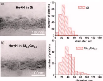
Figure 5 shows a set of typical XTEM images of the He+ H sequentially implanted Si and SiGe samples after the same annealing关Figs.5共a兲and5共b兲兴 and the size histograms describing the populations of platelets in these samples. After annealing at moderate temperature, the mean size of the platelets is significantly larger in SiGe共40 nm兲 than in Si 共27 nm兲. Conversely, the area density of platelets is smaller in SiGe than in Si: 5.5⫻1010and 11⫻1010 cm−2, respectively.
Moreover, the width of the zone in which the platelets are confined is smaller in SiGe than in Si共60 and 80 nm, respec-tively兲. We conclude from these observations that the Ost-wald ripening of platelets created by the sequential implan-tation of He and H is faster in SiGe than in Si.
IV. DISCUSSION
The data on splitting kinetics presented in Fig.1 clearly show that the process of layer transfer depends strongly on the properties of the corresponding materials and the nature
FIG. 4. 共Color online兲 SIMS profiles of H and He in as-implanted and annealed Si and Si0.8Ge0.2 samples. A 1450-Å-thick oxide was removed
before analysis of the samples.
FIG. 5. 共Color online兲 XTEM micrographs of annealed sequentially im-planted samples.
of the implanted species, i.e., H-implant or sequential im-plant He+ H. XTEM images 关Figs. 2共a兲 and 2共b兲兴 do not
show significant differences between the populations of platelets observed in H-only implanted samples, Si and SiGe, after annealing at moderate temperature. The difference in splitting kinetics cannot be directly ascribed to differences in H diffusivity or platelet growth rate as the diffusivities of all relevant species involved in that growth 共H and vacancies兲 are larger in SiGe than in Si. We note, however, that the depth distribution of platelets is wider in SiGe than in Si, an observation consistent with the larger surface roughness of the SiGe samples after splitting.9The reason for slower split-ting in SiGe is not due to the behavior of H-related defects but to the reaction of the material itself to the stress exerted by a given population of defects. Indeed, stress relaxation by straining of the matrix is expected to be easier in SiGe than in Si owing to the weaker Si–Ge bond. An important obser-vation concerns the presence of nanovoids and the platelet-like aligned nanovoids 关Figs.2共d兲 and2共f兲兴 in as-split SiGe when the annealing increases up to 500 ° C. These platelet-like aligned nanovoids might be due to the breaking up of 共001兲 platelets into small pores. That phenomenon was not detected in Si关Fig.2共e兲兴. It is known that the propagation of fracture lines is due to formation of 共001兲 hydrogen-terminated internal surface and pumping of gas共H2兲 in it.11
We speculate that, at the later stages of the layer transfer, due to the lower thermal stability of the Si–H bond the hydrogen-terminated 共100兲 internal surface in Si0.8Ge0.2 changes its
morphology. Si in the matrix tends to close up other nearby Si, resulting in a decrease in the size and density of these platelets. In contrast, for Si, the Si–H bond of 共100兲 hydrogen-terminated internal surface is more stable even at 650 ° C.12 The loss of many platelets favorable for exfolia-tion at this moment provides an explanaexfolia-tion of the slower splitting kinetics in SiGe with the H-only implant.
Thermal annealing of hydrogen implanted Si results in significant increase in the channeled-RBS signal. Cerofolini et al.13attributed the origin of this effect to the formation of hydrogen molecules in vacancy agglomeration sites. Our RBS/channeling results in Fig. 3 indicate that significantly stronger reverse annealing effect is observed for the sequen-tially implanted samples, Si, and Si0.8Ge0.2, as compared to H-only ones. Despite a very low level of damage in the as-implanted state for sequential implants, the height of the damage peaks is comparable for both implant types after the short anneal at moderate temperature. The finding is very consistent with the TEM observation that the populations of platelets are much more confined in depth after sequential implantation 共about 60–80 nm in Fig.5兲 than after H-only
implantation共about 210 nm in Fig.2兲. Moreover, TEM also
reveals that the platelets found after sequential implantation are much larger than those found after H-only implantation after the same annealing conditions. These two characteris-tics, larger platelets and better in-plane confinement of these platelets, explain well why splitting occurs faster after se-quential implantation than after H-only implantation. It is well known that implantation with any kind of ion leads to formation of high strain closer to the implanted range. Dur-ing sequential implantation, H is introduced in the region,
which is already strained by previous implantation of He. So, this region could be “doubly” strained. Of course, this works only in the case of sequential implantation and cannot be applied for H-only implantation. Alternatively, SIMS results show that the total redistribution of He during annealing oc-curs with characteristics consistent with the diffusion and trapping of the He atoms in a sharp region close to the H profile共Fig.4兲. The “double strain” effect and massive
trans-fer of He toward the H-rich region allow a faster growth of the H and He related platelets. Recent and in-depth charac-terization of quite similar samples by positron Dopler broad-ening spectroscopy 共DBS兲 suggests that hydrogen atoms in-teract with the damage previously created by He implantation, producing more stabilized vacancylike defects, a finding consistent with our own observations.14
Diffusivity arguments only cannot be brought to the forefront to explain the different behaviors in splitting kinet-ics between Si and SiGe after sequential implantation since we ruled them out to compare splitting characteristics be-tween H-only and sequential implantations in two materials. The migration length of He is larger in SiGe than in Si as measured by our SIMS results. However, for both in Si and SiGe, the phenomenon is not limited by He diffusion only as all the He atoms should be transferred during annealing from the implanted region toward the H-rich region. Interestingly, TEM shows that after the same implantation and annealing conditions, the platelets are significantly larger, in smaller density, and confined within a thinner layer in SiGe than in Si共Fig.5兲. In other words, the Ostwald ripening of the
plate-lets, known to be at the origin of the formation of microc-racks and further splitting, goes faster in SiGe than in Si after sequential implantation, while this could not be evidenced after H-only implantation.
The nucleation and/or the Ostwald ripening of the He–H platelets are/is limited by the availability and diffusivity of one of the species involved in that competitive growth. Plate-let nucleation and growth occur through the coprecipitation of gas atoms共H and/or He兲 and vacancies.11,15Our TEM and SIMS results show that the behavior of H is quite similar in H-only implanted Si and SiGe samples after annealing at moderate temperature, although some small differences in binding energies exist. We do not expect that He behaves radically differently in SiGe than in Si. Thus, we are left with the possibility that vacancies may play the central role in controlling the kinetics of platelet growth and splitting. The formation of vacancies and vacancy clusters has been studied in detail in SiGe.16It is known that the most abundant defect is a monovacancy surrounded by four Ge atoms, whose for-mation energy is 1 eV lower than that of V – Si4 due to the
weakening of the atomic bonding. Consequently at any given temperature the equilibrium concentration of vacancies is higher in SiGe alloys than in pure Si layer, and this facilitates the nucleation and/or increases the growth rate of the gas-filled cavities during annealing and leads to faster splitting in SiGe.
That result does not contradict that for H-only implanted samples. In the sequentially implanted samples, the fracture line was already observed after annealing at moderate tem-perature 共300–400 °C兲 due to the massive transfer of He
toward the H-rich region. So the layer transfer takes place at the temperature significantly lower than that corresponding to the dissolution of fracture defining共001兲 platelets in SiGe with H-only implantation, i.e., near 500– 550 ° C.
V. SUMMARY
The mechanism of the Si0.8Ge0.2 layer transfer in the Smart Cut™ technology for H-only and sequential He+ H implants was studied using a wide range of techniques. Tak-ing into account recently published results, we propose a scenario that explains the observed behavior. For H-only im-plants, the slower splitting in SiGe than in Si is due to the reaction of the material itself to the stress exerted by a given population of defects in this material. Alternatively, after se-quential He+ H implantation, this effect is overcompensated by the faster growth kinetics of gas-filled platelets, a behav-ior we correlated with the “double strains” effect and fast diffusion and total getting of He into the H-rich and/or V-rich regions. In all cases, sequential implantation at low dose per-mits faster splitting kinetics in Si and SiGe than H-only im-plantation. Moreover, the larger concentration of vacancies available in the SiGe samples facilitates the nucleation and/or increases the growth rate of the gas-filled cavities dur-ing annealdur-ing, leaddur-ing to faster splittdur-ing in SiGe sequentially implanted sample with regard to pure Si.
1J. Welser, J. L. Hoyt, and J. F. Gibbons,IEEE Electron Device Lett.15,
100共1994兲.
2W. Xiong, C. R. Cleavelin, P. Kohli, C. Huffman, T. Schulz, K. Schruefer,
G. Gebara, K. Mathews, P. Patruno, I. Cayrefourcq, M. Kennard, C. Ma-zure, K. Shin, and T.-J. King Liu,IEEE Electron Device Lett.27, 612 共2006兲.
3A. V-Y. Thean, D. Zhang, V. Vartanian, V. Adams, J. Conner, M.
Canonico, H. Desjardin, P. Grudowski, B. Gu, Z.-H. Shi, S. Murphy, G. Spencer, S. Filipiak, D. Goedeke, X-D. Wang, B. Goolsby, V. Dhandapani,
L. Prabhu, S. Backer, L-B. La, D. Burnett, T. White, B.-Y. Nguyen, B. E. White, S. Venkatesan, J. Mogab, I. Cayrefourcq, and C. Mazure, VLSI Tech. Symp. Proc., 2006, p. 130.
4F. Andrieu, T. Ernst, O. Faynot, Y. Bogumilowicz, J.-M. Hartmann, J.
Eymery, D. Lafond, Y.-M. Le Vaillant, C. Dupre, R. Powers, F. Fournel, C. Fenouillet-Beranger, A. Vandooren, B. Ghyselen, C. Mazure, N. Kern-evez, G. Ghibaudo, and S. Deleonibus, Proceedings of the IEEE Interna-tional SOI Conference, 2005, p. 223.
5B. Ghyselen, J.-M. Hartmann, T. Ernst, C. Aulnette, B. Osternaud, Y.
Bogumilowicz, A. Abbadie, P. Besson, O. Rayssac, A. Tiberj, N. Daval, I. Cayrefourcq, F. Fournel, H. Moriceau, C. Di Nardo, F. Andrieu, V. Pail-lard, M. Cabié, L. Vincent, E. Snoeck, F. Cristiano, A. Rocher, A. Ponchet, A. Claverie, P. Boucaud, M.-N. Semeria, D. Bensahel, N. Kernevez, and C. Mazure,Solid-State Electron.48, 1285共2004兲.
6L. J. Huang, J. O. Chu, D. F. Canaperi, C. P. D’Emic, R. M. Anderson, S.
J. Koester, and H.-S. Philip Wong,Appl. Phys. Lett.78, 1267共2001兲.
7G. Taraschi, A. J. Pitera, L. M. McGill, Z-Y. Cheng, M. L. Lee, T. A.
Langdon, and E. A. Fitzgerald, Novel Materials and Processes for Ad-vanced CMOS, MRS Symposia Proceedings, Vol. 745共Materials Research Society, Pittsburgh, 2003兲, p. N4.7.1.
8R. Singh, I. Radu, M. Reiche, R. Scholz, D. Webb, U. Gösele, and S. H.
Christiansen, Mater. Sci. Eng., B 124–125, 162共2004兲.
9P. Nguyen, C. Aulnette, E. Guiot, N. Daval, K. K. Bourdelle, I.
Cayre-fourcq, C. Deguet, S. Sartori, A. Tauzin, C. Lagahe-Blanchard, and A. Soubie, Silicon-on-Insulator Technology and Devices XII, ECS Proceed-ings, Vol. 2005-03共The Electrochemical Society, Pennington, NJ, 2005兲, p. 185.
10J. Grisolia, G. Ben Assayag, A. Claverie, B. Aspar, C. Lagahe, and L.
Laanab,Appl. Phys. Lett.76, 852共2000兲.
11S. Personnic, K. K. Bourdelle, F. Letertre, A. Tauzin, N. Cherkashin, A.
Claverie, R. Fortunier, and H. Klocker,J. Appl. Phys.103, 023508共2008兲.
12M. K. Weldon, V. E. Marsico, Y. J. Chabal, A. Agarwal, D. J. Eaglesham,
J. Sapjeta, W. L. Brown, D. C. Jacobson, Y. Caudano, S. B. Christman, and E. E. Chaban,J. Vac. Sci. Technol. B15, 1065共1997兲.
13G. F. Cerofolini, L. Meda, R. Balboni, F. Corni, S. Frabboni, G. Ottaviani,
R. Tononi, M. Anderle, and R. Canteri,Phys. Rev. B46, 2061共1992兲.
14C. Macchi, S. Mariazzi, G. P. Karwasz, R. S. Brusa, P. Folegati, S.
Frab-boni, and G. Ottaviani,Phys. Rev. B74, 174120共2006兲.
15C. Villeneuve, K. K. Bourdelle, V. Paillard, X. Hebras, and M. Kennard,J.
Appl. Phys.102, 094905共2007兲.
16M. Rummukainen, J. Slotte, K. Saarinen, H. H. Radamson, J. Hallstedt,
and A. Yu. Kuznetsov,Phys. Rev. B73, 165209共2006兲.