HAL Id: hal-01513102
https://hal.univ-lorraine.fr/hal-01513102
Submitted on 24 Apr 2017
HAL is a multi-disciplinary open access
archive for the deposit and dissemination of
sci-entific research documents, whether they are
pub-lished or not. The documents may come from
teaching and research institutions in France or
abroad, or from public or private research centers.
L’archive ouverte pluridisciplinaire HAL, est
destinée au dépôt et à la diffusion de documents
scientifiques de niveau recherche, publiés ou non,
émanant des établissements d’enseignement et de
recherche français ou étrangers, des laboratoires
publics ou privés.
Effects of structural defects and polarization charges in
InGaN-based double-junction solar cell
Abdoulwahab Adaine, Sidi Ould Saad Hamady, Nicolas Fressengeas
To cite this version:
Abdoulwahab Adaine, Sidi Ould Saad Hamady, Nicolas Fressengeas. Effects of structural defects and
polarization charges in InGaN-based double-junction solar cell. Superlattices and Microstructures,
Elsevier, 2017, 107, pp.267-277. �10.1016/j.spmi.2017.04.025�. �hal-01513102�
Effects of structural defects and polarization charges in InGaN-based double-junction
solar cell
Abdoulwahab Adainea,b, Sidi Ould Saad Hamadya,b, Nicolas Fressengeasa,b
aUniversit´e de Lorraine, Laboratoire Mat´eriaux Optiques, Photonique et Syst`emes, Metz, F-57070, France bLaboratoire Mat´eriaux Optiques, Photonique et Syst`emes, CentraleSup´elec, Universit´e Paris-Saclay, Metz, F-57070, France
Abstract
The performance of a double heterojunction solar cell based on Indium Gallium Nitride (InGaN) including a tunnel junction was simulated. The most challenging aspects of InGaN solar cells development being the crystal polarization and structural defects detrimental effects, their impact on the solar cell performances has been investigated in detail. The solar cell simulation was performed using physical models and InGaN parameters extracted from experimental measurements. The optimum efficiency of the heterojunction solar cell was obtained using a multivariate optimization method which allows to simultaneously optimize eleven parameters. The optimum defect free efficiency obtained is 24.4% with a short circuit current JSC= 12.92mA/cm2, an open circuit voltage VOC= 2.29V and a fill factor FF = 82.55%. The performances evolution as functions of the polarization and the defects types and parameters was studied from their maximum down to as low as a 2% efficiency.
Keywords: Simulation, Optimization, Solar cell, InGaN, Heterojunction, Tunnel, Polarization, Defects
1. Introduction
Among the materials currently being studied for high effi-ciency solar cells lies the Indium Galium Nitride (InGaN) al-loy. Indeed, InGaN possesses unique properties, such as its wide band-gap that is tunable from 0.7 eV to 3.4 eV [1]. It also presents strong interatomic bonds and high thermal con-ductivity [2], which makes it an ideal material for photovoltaic solar panels resistant to high energy radiation.
Several p-n and p-i-n homojunction and heterojunction struc-tures were studied. The strucstruc-tures with low Indium composi-tion have conversion efficiencies below 5% [3,4]. Indeed, in practice, the InGaN layers with a high concentration of Indium are very difficult to achieve today. For relatively high-Indium-content structures, Doolittle et al. [5] theoretically showed that a p-i-n structure having an Indium composition of 60% exhibits
∗Corresponding author
Email addresses:[email protected] (Abdoulwahab Adaine),[email protected] (Sidi Ould Saad Hamady),[email protected] (Nicolas Fressengeas)
a maximum efficiency of about 19%. Our previous studies [6,7] have shown that single junction structures have conver-sion efficiencies not exceeding 20%. The p-n structure presents an optimal efficiency of 17.8% while that of a p-i-n structure is 19.0%. These previous works, using empirical parameters and models, demonstrated that the theoretical maximum efficiency of a single junction is limited to about 20%.
In this paper, we simulate and optimize an InGaN-based dual-junction solar cell including a tunnel junction. This allows the conversion of different parts of the solar spectrum, thus en-hancing the solar light absorption efficiency and the photocar-riers transport. Photovoltaic panels using such solar cells can potentially achieve efficiencies exceeding those of systems that use conventional single junction solar cells.
In the past, only two papers on InGaN-based double-junction solar cells have been published. A first study published in 2008 [8] reports a dual-junction InGaN solar cell with a conversion efficiency of 35.1%. Another similar study published in 2016 [9] confirms these results with a roughly similar efficiency of
34.9%. In these works the two subcells of the solar cell are studied separately. The tunnel junction between the two sub-cells is thus not included in the simulations. The effects related to the junction, such as the electrical resistance, the disconti-nuity of the bands, are thus ignored. Furthemore, the physical parameters of the material used, as well as the optical proper-ties, notably the refractive index, are not reported. Furthermore, the authors did not take into account the structural defects in the InGaN layers and their polarization.
Moreover, the optimum efficiency obtained results from a parametric analysis which obviously does not allow a rigorous optimal efficiency of the solar cell. Indeed, parametric opti-mization can optimize only one parameter at a time, it thus does not allow to take into account the dependencies of optimized parameters.
We thus propose here a new approach which consists in performing a global simulation of the complete InGaN-based double-junction solar cell, including the tunnel junction, us-ing rigorous physical models and empirical material parame-ters, and including structural defects and polarization effects.
Indeed InGaN is usually grown on lattice-mismatched Sap-phire (Al2O3) or GaN/SapSap-phire substrates by MOVPE [10]. Thus, during the growth, a relaxation occurs beyond a certain thickness called ”critical thickness”[11–13], resulting in a high density of dislocations and other structural defects in the InGaN layers, which impacts the solar cell performances. In addition to the defects, InGaN presents a spontaneous polarization due to the intrinsic asymmetry of the bonds in the wurtzite crystal structure, as well as a piezoelectric polarization mainly due to the lattice mismatch between the layers [14,15].
The device is simulated in the framework of a drift-diffusion model using the Atlas device simulation framework from the Silvaco company. It is the most commonly used model to ac-curately describe the fundamental physics of semiconductor-based devices. For the carrier mobility, we use the classic model of Caughey-Thomas in which the carrier mobility is a function of doping and temperature [16]. In order to model the losses in the structure, we take into account the
Shockley-Read-Hall (SRH) [17] and direct Auger recombination models using Fermi statistics. An empirical model of the absorption of light using and interpolating experimental data was used [18] and combined to a precise model for the refractive index initially developped for GaN [19]. When the direct experimental data are not available, the InGaN parameters values are determined using Vegard’s law linear interpolation between InN and GaN binaries values, except for the bandgap (Eg) and the electronic affinity (χ), where we used a quadratic modified Vegard’s law with a bowing parameter of b= 1.43 eV for the bandgap and
b= 0.8 eV for the electronic affinity[18]. All these physical models and dependent material parameters are detailed in our previous work [6,7] and summarized in table1.
The optimization of the device is done with rigorous math-ematical methods. The objective is to find the optimal effi-ciency of the solar cell by simultaneously optimizing a given set of physical and geometrical parameters of the cell. We have, for this solar cell, optimized simultaneously eleven parameters. With that many parameters to optimize, a careful fine tuning of the previously used optimization algorithms was necessary in order to ensure their convergence while keeping a reasonable computing time, which can be as high as 30 hours per simula-tion.
This optimization work was realized with a Python package that we developed using the SciPy optimizers[20]. This pack-aged source code will be released to the photovoltaic commu-nity soon.
The paper is organized as follows. In the next section 2, we describe the solar cell structure as well as the InGaN struc-tural properties that can limit the performance of the solar cell, including structural defects and spontaneous and piezoelectric polarizations. In section 3, we present the optimal results ob-tained and discuss the effects of the polarization and structural defects on the performance of the solar cell, before concluding.
Parameters[18] InN GaN
Bandgap Eg(eV ) 0.7 3.42
Electron affinity χ (eV ) 5.6 4.1
Hole and electron lifetime (ns) 1 1
Dielectric constant 15.3 8.9
Nc(cm−3) 9.1 × 10¹⁷ 2.3 × 10¹⁸
Nv(cm−3) 5.3 × 10¹⁹ 4.6 × 10¹⁷
Physical model
Charge carrier mobility Caughey-Thomas Model [21]
Absorption Coefficient Phenomenological Model [18]
Refraction Index Adachi Model [19]
Table 1: Parameters of InN an GaN and significant physical model used in the simulations of the solar cell structure
2. Solar cell, polarization and defect modeling
2.1. Solar cell structure
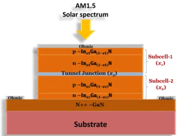
The modeled solar cell is based on an InGaN-made double junction structure shown on Figure 1. This structure is com-posed of two vertically stacked p-n junctions with a top wide bandgap cell, named subcell-1 in the following, and a bot-tom narrower bandgap cell, named subcell-2, both being con-nected by a tunnel junction. The difference in the bandgaps is obtained by changing the Indium composition x of InGaN. The structure is studied under an AM1.5 illumination (about 100mW/cm2). The high-energy photons are absorbed by the
top subcell (subcell-1) while those of lower energies are trans-mitted through the junction to be absorbed by the bottom sub-cell (subsub-cell-2). The solar sub-cell structure therefore absorbs a larger solar spectrum and can thus produce more energy than a single junction cell, provided the current can be matched be-tween the two subcells.
Indeed, the two subcells being connected in series, the sub-cell that produces the smallest current limits the maximum cur-rent that can flow through the solar cell. Therefore, the opti-mum performance of the cell strongly depends on the subcells electrical interconnection and their respective optimal currents. To achieve that fine tuning, the two subcells are connected by a tunnel junction, consisting of yet another p-n junction built in the opposite direction to that of the two subcells wich are designed for photocurrent generation. We designed here a p-n junction whose Indium composition can be different from that
Figure 1: Solar cell structure with two p-n junctions (subcell-1 and subcell-2) connected by a tunnel junction. The cell is realized on a substrate via a heavily doped GaN buffer layer. x1represents the composition of the subcell-1, x2the
Indium composition of subcell-2 and x3the induium composition of the tunnel
junction. The structure is under AM1.5 illumination.
of the subcells and that includes highly doped p++ and n++ layers. Therefore, This junction space-charge region is spatially narrow and its Fermi level is located both in the conduction and valence band: the bottom of the conduction band is on the same level as the top of the valence band.This way, the charge carriers can cross the potential barrier by tunneling.
Finally, the device proposed here can be realized in practice using the conventional InGaN growth on insulating substrates such as Sapphire (Al2O3) or SiC via a GaN or similar heavily
doped buffer layer.
2.2. Spontaneous and piezoelectric polarizations
The InGaN crystal structure belongs to the wurtzite group [22]. It is a non-centrosymmetric structure having two types of polarities according to the arrangement of atoms of Gallium and Nitrogen during the epitaxial growth. They are called Ga-face polarity if the last epitaxially grown atomic layer is composed of Gallium atoms and N-face polarity if the last epitaxially grown atomic layer is composed of Nitrogen atoms [23]. This polarity will generate a spontaneous polarization (PSP) in the structure, spatially separating electrons and holes and thus creating an accumulation of charges at the InGaN sur-face.
InN GaN e31(C/m2) -0.41 -0.34 e33(C/m2) 0.81 0.67 c13(GPa) 94 100 c33(GPa) 200 392 Psp(C/m2) -0.042 -0.034
Table 2: Experimental data of piezoelectric parameters and spontaneous polar-ization values for InN and GaN [26].
In addition to the spontaneous polarization, the lattice mis-matched between different composition layers induces strain and thus piezoelectric polarization. This polarization also re-sults in a displacement of electrons and holes at the surface of the layers and therefore may either reduce or enhance the total polarization [23]. Thus, without external polarization, the total polarization of the structure is equal to the sum of the sponta-neous and piezoelectric polarizations.
Charge accumulation at the extremities of the structure can then change the electrical properties of the solar cell and the re-sulting photovoltaic performances. Indeed, if the electric field associated with the total polarization is in the same direction as the field generated in the space-charge region of the PN junc-tion, the polarization could improve the performance of the cell, or reduce it otherwise.
The spontaneous polarization (Psp) is quadratically interpo-lated from the modified Vegard’s law with a bowing factor of
b= 0, 038C/m2[24,25]:
PspInGaN= xPspInN+ (1 − x)PspGaN− bx(1 − x), (1)
where x is the Indium composition of InxGa1−xN, PspInGaN is the spontaneous polarization of InxGa1−xNwhile PspInN and and PspGaN are the spontaneous polarizations of InN and GaN binaries. Their values are given in Table2.
The piezoelectric polarization (Ppi) is linearly interpolated by Vegard’s law [24]:
PpiInGaN= xPInN
pi + (1 − x)PpiGaN, (2)
where PInGaNpi is the piezoelectric polarization of InxGa1−xN,
0.0 0.1 0.2 0.3 0.4 0.5 0.6 0.7
Indium Concentration (x)
0 20 40 60 80 100 120 140Critical Layer Thickness (nm)
Figure 2: The critical layer thickness for InxGa(1−x)N/GaN layer as a function
of the Indium composition using a Fischer model [27]. Blue circles represent experimental measurements from [13] and the red diamonds the experimental measurements from [12].
PpiInN and PpiGaN are the piezoelectric polarizations of InN and GaN binaries. The latter are evaluated from piezoelectric con-stants and lattice parameters [22]:
Ppi= 2 ×
as− a0
a0
× (e31 −c13
c33× e33), (3)
where e31 and e33 are piezoelectric constants; c13 and c33 are elastic constants; asand a0are the lattice parameters of the
substrate and of the material layer respectively. Their values are summarized in Table2.
2.3. Critical thickness
In our modeling conditions, the spontaneous polarization is applied throughout the structure, while the piezoelectric polar-ization is applied only to the strained layers. In order to deter-mine if a layer is strained or relaxed, we refer to the experimen-tal measurements of critical thicknesses as a function of Indium composition. Since no measurements has been done for high Indium content layers, we have fitted the experimental data re-ported in [12] and [13] by a Fischer model [27] to extrapolate the critical thicknesses for high Indium content layers (Figure
2). For the extrapolation based on the measurements reported in [13], the critical thickness corresponding to an Indium compo-sition of x= 0.6 would be about 30nm, while it would be closer
to 10nm for that based on [12]. Therefore, for our simulations, we considered that all layers with a thickness less than 10nm are strained and thus that layers having a thickness greater than 10nm are relaxed. This layer relaxation induces a high density of dislocations and other structural defects in the epitaxial layer.
2.4. Structural defects
Among the defects in III-Nitride alloys, and particularly evi-denced in GaN, one can cite point antisites and interstitials de-fects, threading dislocations [28], stacking faults [29], stacking mismatch boundaries [30], grain boundaries [31], nanopipes and inversion domains[32]. All these defects cause perturba-tions in the periodicity of the crystal and affect the electronic properties of the devices. The defect whose associated en-ergy lies in the bandgap, exchange with the conduction and valence bands through the emission and capture of electrons or/and holes. Garni et al. [33], showed that threading disloca-tions in GaN act as nonradioactive centers and diffusion centers in electron transport[34]. Moreover, Garni et al. also showed that these dislocations defects cause nonradioactive recombi-nation which causes crystal heating up and thus significantly influences the performances of the device.
According to calculations by Neugebauer and Van de Walle [35], the formation energy of GaN point defects depends on the position of the Fermi level. The type of the defects usu-ally observed in GaN thus depends on the doping type of the layer. This study shows that, for p-type doping, the Nitrogen vacancy have the lowest energy and are therefore most likely to be present in this layer while for n-type doping, Gallium va-cancy are dominating. The Nitrogen vacancies being n-type and the Gallium vacancies being p-type, one can conclude that on p-type layers, the donor-type defects will be dominant, while, in n-type layers, the acceptor-type defects will.
Stampf et al. [36] also showed that, for InN, the Nitrogen vacancies have a lower energy than other defects in the p-type layers and thus are more likely to be present. It is then assumed that InGaN has the same types of defects as GaN and InN. We therefore consider in our simulations the donor-type defects in
p-type layers and acceptor-type defects in n-type layers. Furthermore and to take into account the disorder due to dis-locations, the defect density of states is defined as a continuous function of the energy. It is a combination of exponentially de-caying band tail states and Gaussian distributions states within the bandgap. Band tail states represent the shallow states in the bandgap and Gaussian distributions represent the deep ones. They both impact the effective charge mobility through the cap-ture and recombination of opposite charges. The total density of states is thus composed of four bands: two band tails and two bands of deep levels.
3. Influence of defect and polarization on efficiency
3.1. Solar cell optimization
The simulated and optimized cell structure is shown schematically in Figure1. It includes three different Indium compositions: subcell-1 has an x1 Indium composition and
subcell-2has an x2one while the junction tunnel can exhibit
a yet different x3Indium composition.
The 11 parameters for which we sought the optimal values are the the 2 layer thicknesses and dopings for each PN junc-tion along with their composijunc-tions. These 10 parameters are in-cluded globally in the optimization process along with the tun-nel junction Indium composition. The thicknesses and dopings of the tunnel junction have not been included in the optimiza-tion process because our simulaoptimiza-tions have shown that they need to be as highly doped and thin as the technology allows it.
All the 11 optimization parameters have been constrained within a variation domain, which is the interval in which they are meaningful in physical and technological terms. The In-dium compositions are allowed within the full range: xi ∈ [0, 1], ∀i ∈ {1, 2, 3}. The InGaN layer n-type and p-type dop-ings (Nd and Na) minimum allowed values are chosen to be the minimal residual doping of 1016cm−3, as usually measured in this material. Their maximum values are, on their side, set to 1019cm−3, which is the highest doing value used. To put it shortly: Nd∈ [1016, 1019]cm−3and Na∈ [1016, 1019]cm−3. For
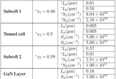
Subcell 1 ∗x1= 0.40 ∗L p(µm) 0.01 ∗L n(µm) 0.58 ∗N a(cm−3) 8.04 × 10¹⁸ ∗N d(cm−3) 2.38 × 10¹⁶ Tunnel cell ∗x3= 0.5 Ln(µm) 0.005 Lp(µm) 0.005 Nd(cm−3) 5.00 × 10¹⁹ Na(cm−3) 5.00 × 10¹⁹ Subcell 2 ∗x2= 0.59 ∗L p(µm) 0.57 ∗L n(µm) 0.01 ∗N a(cm−3) 2.51 × 10¹⁸ ∗N d(cm−3) 1.00 × 10¹⁷ GaN Layer Ln(µm) 0.16 Nd(cm−3) 1.00 × 10¹⁹
Table 3: Optimized parameters of the heterojunction InGaN solar cell. The parameters marked with an asterisk are the eleven simultaneously optimized parameters, the other parameters being fixed. x1, x2and x3are the Indium
com-positions for subcell-1, subcell-2 and tunnel junction respectively (see figure1).
Lpand Lnare the InGaN layer thicknesses of the P and N layers respectively. Naand Npare the dopings of the P and N layers respectively. The optimum
efficiency found is 24.4%, associated to a JSC= 12.92mA/cm2 short circuit
current, a VOC= 2.287V open circuit voltage and a FF = 82.55% fill factor.
the InGaN layer thicknesses (Lpand Ln), we chose to set the minimum values to 10nm and the maximum values to 1µm. Therefore: Lp∈ [0.01, 1.00]µm and Ln∈ [0.01, 1.00]µm.
Finally, for the optimizing algorithm to work as expected, the sought parameters should have similar variation ranges. There-fore, the Indium composition and the layer thicknesses are nor-malized to 1, their maximum value. For doping, the normal-ization is logarithmic (log10) and normalized to 19, its
maxi-mum value. The mathematical optimization methods used for optimization are detailed in our recent published work [6,7]. Optimization is run several times with several starting points randomly chosen to ensure that the optimum obtained is abso-lute.
Using this procedure, a global maximum cell efficiency of 24.4% is found. Associated to this maximum efficiency, the dual junction solar cell main electrical characteristics at the op-timum are the short circuit current JSC = 12.92mA/cm2, the open circuit voltage VOC = 2.287V and the fill factor FF = 82.55%. The optimal values obtained for the free parameters are given in Table3. Figure3 shows the current-voltage and power-voltage characteristics of the this optimal solar cell.
0.0 0.5 1.0 1.5 2.0 2.5 Voltage (
V
) 0 2 4 6 8 10 12 14 C ur re nt (mA/c
m
2) 5 10 15 20 25 Po w er (mW
/cm
2)Figure 3: Current-voltage and power-voltage charateristics of the solar cell at the optimum.
By comparison, previous simulation works for InGaN-based double-junction solar cells obtained a higher efficiency [8,9] of 35.1%. This is due to the fact that this work did not take into account the tunnel junction as itself. The two subcells were simulated separately and the effects of the series resistance and tunnel junction ignored.
In addition, our work is based on an empirical conduction and absorption model directly deduced from experimental data, associated to a rigorous optimization procedure. Therefore, we expect the obtained optimal efficiency to be on one side actually optimal and, on the other side, not overestimated.
3.2. Spontaneous and Piezoelectric polarization
Once the optimal solar cell found, the effects of the po-larization charges on its performances have been analyzed. As pointed out above, the spontaneous polarization is applied throughout the structure while the piezoelectric polarization is applied only to the constrained layers. subcell-2 has an op-timum thickness of 0.56µm, and is thus relaxed, as deduced from figure2and previously discussed in section2.3. The tun-nel junction, at the bottom, has a thickness of 10nm, so it is a constrained layer. The subcell-1 has a lattice parameter very close to that of the tunnel junction, it is also constrained. In short, the piezoelectric polarization is considered for the tunnel junction and subcell-1 only.
0.0 0.5 1.0 1.5 2.0 2.5 Voltage (
V
) 0 2 4 6 8 10 12 14 C ur re nt (mA/c
m
2) 1.0 1.8 2.0 3.0(a) Current-voltage characteristics with different polarization charges.
>> >>
Subcell-2 Tunnel Junction
Subcell-1
(b) Conduction band diagrams in the tunnel junction with different polarization charges.
Figure 4: Impact of total polarization on the performances of the solar cell. The normalized value of 1.0 corresponds to the value in C/m2, obtained by
the sum of the spontaneous and piezoelectric polarization given respectively by equations (1) and (2). To evidence the impact of a strong polarization, it is grad-ually increased up to 3 times the total polarization. subcell-1 is on the left of the figure, while subcell-2 is on its right, the tunnel junction being sandwiched between the two.
Figure4(a)shows the I-V curves for solar cells with different polarization charge. The normalized value of 1.0 corresponds to the value in C/m2, obtained by the sum of the spontaneous
and piezoelectric polarization given respectively by equations (1) and (2). For a small polarization, a normalized value of 1.0, the solar cell performances barely change, the optimal ef-ficiency dropping from 24.4% to 23.3%. However, should the polarization charges be higher, a sharp decrease in the open cir-cuit voltage VOC would be seen while the short circuit current
JSCwould remains constant. In addition, for high polarizations, a change in the shape of the curve would be observed, consid-erably degrading the fill factor.
To explain these behaviors, we have analyzed the conduction band in the tunnel junction with various polarization charges, as is shown in figure4(b). The polarization charges bend the con-duction band at the interface between the tunnel junction and
subcell-2; the bend curvature increasing with the polarization. This causes charges to accumulate at this interface, which in turn create an electric field. This field, induced by the polar-ization, is in the direction opposite to that of the PN junction internal field. It thus tends to lower the total integrated electric field in the cell, which explains the decrease in the open circuit voltage VOC.
Moreover, the presence of this induced field reveals a reverse biased diode, which opposes the efficient collection of the car-riers. A threshold effect appears: when the induced field is less than the electric field of the cell, a deformation of the I-V curve is observed which severely degrades the fill factor and thus de-creases the solar cell efficiency though no change on the short circuit current is JSCis observed; on the contrary, if the induced field is largely greater than that of the cell, the deformation of the I-V curve also results a decrease of the JSC. Indeed, the induced field opposes efficient collection of the carriers. This leads to a decrease of the current in the subcell-2. This latter then imposes its low current to the whole structure.
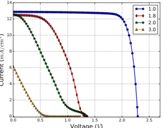
3.3. Deep and band tail defects
As for polarization, structural defects play a central role in an InGaN solar cell operation. The InGaN layer composing
subcell-2being relaxed, the dislocations generated are similar to line charges and are an important source of defects, consid-erably reducing the mobility of the charge carriers and the effi-ciency of the solar cell.
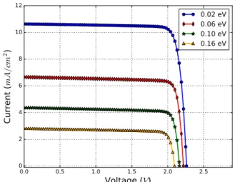
In figure5, the impact of the Urbach band tail energy on the cell performances was studied. In figure6, it is the impact of the deep defects Gaussian distribution that was studied. Figures
5(a)and6(a)show the different current-voltage characteristics of the solar cell, while figures5(b)and6(b)show the variations of JSCand VOC.
Band tails reflect the state of disorder of the material. The characteristic energies of the band tails and deep defects usually increase with the Indium composition. This is the reason why their influence on the solar cell performances was studied.
The increase of the Urbach energy as well as that of the de-cay energy (Figures5(a)and6(a)) leads to a decrease of the JSC while the VOCremains almost constant (Figures5(b)and6(b)). Indeed, an increase of the Urbach energy implies a reduction in the optical gap owing to the presence of states in the InGaN bandgap, leading to a higher probability of carrier recombina-tion. In the same way, for the deep states, the increase of the decay energy also leads to an increase of the state density in the bandgap and therefore to a higher probability of recombination of the carriers. Both these effects thus result in the decrease of the short circuit current JSC.
However, it can be noted the an increase in the disorder – in the Urbach energy– degrades the solar cell performances much more than a deep states decay energy increase. Indeed, for an Urbach energy of 60meV, the short circuit current JSC drops from more than 10 to 6.65mA/cm2, while the variation of
the decay energy, between 20meV and 160meV only induces a slight decrease in the same short circuit current JSC from 12.8 down to 10.5mA/cm2. In InGaN solar cells, material disorder
is therefore more detrimental to the performances than deep de-fects states. 0.0 0.5 1.0 1.5 2.0 2.5 Voltage (
V
) 0 2 4 6 8 10 12 C ur re nt (mA/c
m
2) 0.02 eV 0.06 eV 0.10 eV 0.16 eV(a) Current-voltage characteristics with various Urbach energy of the band tail.
0.00 0.05 0.10 0.15 0.20 Decay energy (
eV
) 0 2 4 6 8 10 12J
SC (mA/c
m
2) 0 1 2 3 4 5 6V
OC (V
) JSC VOC(b) Variation of JSCand VOCas a function of the Urbach energy of the band tail.
Figure 5: Impact of the band tail Urbach energy on the performances of the solar cell. The efficiency drops from 20.54% down to 4.89% for an Urbach energy varying from 0.02eV up to 0.16eV. The fill factor remains unchanged around 82%. The capture cross-sections are taken equal to 1× 10⁻¹⁴cm2, the
band tail state densities are taken equal to 2.3 × 1018cm2for the valence band
0.0 0.5 1.0 1.5 2.0 2.5 Voltage (
V
) 0 2 4 6 8 10 12 14 C ur re nt (mA/c
m
2) 0.02 eV 0.06 eV 0.10 eV 0.16 eV(a) Current-voltage characteristics with various decay energy of the Gaussian distribution. 0.00 0.05 0.10 0.15 0.20 Decay energy (
eV
) 10.0 10.5 11.0 11.5 12.0 12.5 13.0 13.5 14.0J
SC (mA/c
m
2) 1.0 1.5 2.0 2.5 3.0V
OC (V
) JSC VOC(b) Variation of JSCand VOCas a function of the decay energy of the Gaussian
distribution.
Figure 6: Impact of the Gaussian distribution decay energy on the performances of the solar cell. The efficiency is slightly degraded from 22.90% down to 19.45% for a defect decay energy varying from 0.02eV up to 0.20eV, the fill factor remaining unchanged around 81%. The capture cross-sections are taken equal to 1× 10⁻¹⁴cm2. The energies that correspond to the Gaussian
distribu-tion peaks are fixed at 0.6eV, the Urbach energy of the band tail is set at 0.05eV, the defect density of donor-type is equal to 1× 1018cm2. The defect density of
acceptor-type is equal to 1× 1017cm2.
1014 1015 1016 1017 1018 1019
Defect Density (
cm
−3/eV
)0 5 10 15 20 25 Ef fic ie nc y (% )
(a) Solar cell efficiency as a function of the defect density of donor-type states in a Gaussian distribution.
1014 1015 1016 1017 1018 1019
Defect Density (
cm
−3/eV
)0 2 4 6 8 10 12 14
J
SC (mA/c
m
2) 0.0 0.5 1.0 1.5 2.0 2.5 3.0 3.5V
OC (V
) JSC VOC(b) Variation of JSCand VOCas a function of the defect density of donor-type
states in a Gaussian distribution.
Figure 7: Impact of the defect density of donor-type states in a Gaussian distri-bution on the performance of the solar cell. The defect density of acceptor-type states is constant and equal to 1017cm−3. The capture cross-sections are taken
equal to 10−14cm2. The energies that correspond to the Gaussian distribution
Finally, in Figure7, the effect of the density of donor-type defects was studied. Figure7(a)shows its impact on the effi-ciency whereas figure7(b)shows its impact on the short circuit current JSC and the open circuit voltage VOC. For donor-like defects, that are mostly found in the p-type layer, it can be ob-served that, when the defects density is less than the doping density in the layer, the efficiency remains close to its optimal value. On the contrary, as soon as the defects density exceeds the doping density, the efficiency of the cell dramatically de-creases as shown in Figure 7(a). Indeed, by their ability to emit or capture free carriers, defects can compensate for in-tentionally introduced donor or acceptor levels. This reduces the mobility of the photogenerated carriers, thus reducing the short circuit current JSC (Figure7(b)) and the solar cell overall efficiency.
4. Conclusion
In this work, a detailed investigation on the performance of an InGaN-based double-junction solar cell was carried out. We have globally simulated the solar cell using empirical InGaN material parameters, to avoid any overestimation in the solar cell performances. In order to take into account the interde-pendence of the solar cell physical and geometrical parameters, ensuring the absoluteness of the optimized photovoltaic perfor-mances, the cell was optimized using a multivariate optimiza-tion algorithm that simultaneously optimizes eleven physical and geometrical parameters. We obtained an optimal efficiency of 24.4%, with a short circuit current JSC = 12.92mA/cm2, an open circuit voltage VOC= 2.287V and a fill factor FF = 82.55%.
We quantitatively investigated the impact on the solar cell performances of the internal polarization and structural defects in InGaN. We have shown that the internal polarization reduces the performance of the cell by inducing an electric field which does not favor an efficient collection of photo-generated car-riers; showing the importance of controlling this polarization when designing the lattice-mismatched solar cell heterostruc-ture. We have also investigated the impact of structural defects
in InGaN, including disorder and deep defects, and correlated their effect to the InGaN doping concentration.
[1] C. Zhang, J. Gwamuri, R. Andrews, J. M. Pearce, Design of Multijunc-tion Photovoltaic Cells Optimized for Varied Atmospheric CondiMultijunc-tions, International Journal of Photoenergy 2014 (2014) e514962.
[2] A. Bhuiyan, K. Sugita, A. Hashimoto, A. Yamamoto, InGaN solar cells: present state of the art and important challenges, IEEE Journal of Photo-voltaics 2 (3) (2012) 276–293.
[3] E. Matioli, C. Neufeld, M. Iza, S. C. Cruz, A. A. Al-Heji, X. Chen, R. M. Farrell, S. Keller, S. DenBaars, U. Mishra, et al., High internal and exter-nal quantum efficiency InGaN/GaN solar cells, Applied Physics Letters 98 (2) (2011) 021102.
[4] M. R. Islam, M. R. Kaysir, M. J. Islam, A. Hashimoto, A. Yamamoto, MOVPE growth of InGaN and fabrication of homo-junction solar cells, Journal of Materials Science & Technology 29 (2) (2013) 128–136. [5] C. A. M. Fabien, W. A. Doolittle, Guidelines and limitations for the
de-sign of high-efficiency InGaN single-junction solar cells, Solar Energy Materials and Solar Cells 130 (2014) 354–363.
[6] S. Ould Saad Hamady, A. Adaine, N. Fressengeas, Numerical simulation of InGaN Schottky solar cell, Materials Science in Semiconductor Pro-cessing 41 (2) (2016) 219–225.
[7] A. Adaine, S. Ould Saad Hamady, N. Fressengeas, Simulation study of a new InGaN p-layer free Schottky based solar cell, Superlattices and Microstructures.
[8] X. Zhang, X. Wang, H. Xiao, C. Yang, J. Ran, C. Wang, Q. Hou, Jinmin Li, Z. Wang, Theoretical design and performance of ingan two-junction solar cells, Journal of Physics D: Applied Physics 41 (24) (2008) 245104. [9] A. Mesrane, A. Mahrane, F. Rahmoune, A. Oulebsir, Theoretical Study and Simulations of an InGaN Dual-Junction Solar Cell, Journal of Elec-tronic Materials (2016) 1–8.
[10] A. S´anchez, M. Gass, A. Papworth, P. Goodhew, P. Singh, P. Ruterana, H. Cho, R. Choi, H. Lee, V-defects and dislocations in InGaN/GaN het-erostructures, Thin Solid Films 479 (1-2) (2005) 316–320.
[11] D. Holec, P. Costa, M. J. Kappers, C. J. Humphreys, Critical thickness calculations for InGaN/GaN, Journal of Crystal Growth 303 (1) (2007) 314–317.
[12] M. J. Reed, N. A. El-Masry, C. A. Parker, J. C. Roberts, S. M. Bedair, Critical layer thickness determination of GaN/InGaN/GaN double het-erostructures, Applied Physics Letters 77 (25) (2000) 4121–4123. [13] C. A. Parker, J. C. Roberts, S. M. Bedair, M. J. Reed, S. X. Liu, N. A.
El-Masry, Determination of the critical layer thickness in the InGaN/GaN heterostructures, Applied Physics Letters 75 (1999) 2776.
[14] Z. Q. Li, M. Lestradet, Y. G. Xiao, S. Li, Effects of polarization charge on the photovoltaic properties of InGaN solar cells, physica status solidi (a) 208 (4) (2011) 928–931.
[15] H. Zhang, E. J. Miller, E. T. Yu, C. Poblenz, J. S. Speck, Measurement of polarization charge and conduction-band offset at ingan/gan
heterojunc-tion interfaces, Applied Physics Letters 84 (23) (2004) 4644–4646. [16] D. Caughey, R. Thomas, Carrier mobilities in silicon empirically related
to doping and field, Proceedings of the IEEE.
[17] H.-Y. Ryu, H.-S. Kim, J.-I. Shim, Rate equation analysis of efficiency droop in InGaN light-emitting diodes, Applied Physics Letters 95 (8) (2009) 081114.
[18] G. Brown, J. Ager III, W. Walukiewicz, J. Wu, Finite element simulations of compositionally graded InGaN solar cells, Solar Energy Materials and Solar Cells 94 (3) (2010) 478–483.
[19] A. B. Djuriˇsi´c, E. H. Li, Modeling the optical constants of hexagonal GaN, InN, and AlN, Journal of Applied Physics 85 (5) (1999) 2848–2853. [20] E. Jones, T. Oliphant, P. Peterson, et al., SciPy: Open source scientific
tools for Python,http://www.scipy.org/ (2001–).
[21] F. Schwierz, An electron mobility model for wurtzite GaN, Solid State Electronics 49 (6) (2005) 889–895.
[22] F. Bernardini, V. Fiorentini, D. Vanderbilt, Spontaneous polarization and piezoelectric constants of III-V nitrides, Physical Review B 56 (16) (1997) R10024–R10027.
[23] L. Liu, J. H. Edgar, Substrates for gallium nitride epitaxy, Materials Sci-ence and Engineering: R: Reports 37 (3) (2002) 61–127.
[24] F. Bernardini, V. Fiorentini, Nonlinear behavior of spontaneous and piezoelectric polarization in III-V nitride alloys, physica status solidi(a) 190 (1) (2002) 65–73.
[25] V. Fiorentini, F. Bernardini, O. Ambacher, Evidence for nonlinear macroscopic polarization in III–V nitride alloy heterostructures, Applied Physics Letters 80 (7) (2002) 1204–1206.
[26] J. Piprek, Semiconductor Optoelectronic Devices: Introduction to Physics and Simulation, Academic Press, 2013.
[27] A. Fischer, H. K ¨uhne, H. Richter, New approach in equilibrium theory for strained layer relaxation, Physical review letters 73 (20) (1994) 2712. [28] D. Kapolnek, X. H. Wu, B. Heying, S. Keller, B. P. Keller, U. K. Mishra,
S. P. DenBaars, J. S. Speck, Structural evolution in epitaxial metalorganic chemical vapor deposition grown GaN films on sapphire, Applied Physics Letters 67 (11) (1995) 1541–1543.
[29] F. Gloux, P. Ruterana, K. Lorenz, E. Alves, A comparative structural in-vestigation of GaN implanted with rare earth ions at room temperature and 500 c, Materials Science and Engineering: B 146 (1–3) (2008) 204– 207.
[30] B. N. Sverdlov, G. A. Martin, H. Morkoc¸, D. J. Smith, Formation of threading defects in GaN wurtzite films grown on nonisomorphic sub-strates, Applied Physics Letters 67 (14) (1995) 2063–2065.
[31] H. Z. Xu, K. Takahashi, C. X. Wang, Z. G. Wang, Y. Okada, M. Kawabe, I. Harrison, C. T. Foxon, Effect of in situ thermal treatment during growth on crystal quality of GaN epilayer grown on sapphire substrate by MOVPE, Journal of Crystal Growth 222 (1–2) (2001) 110–117. [32] F. A. Ponce, W. T. Young, D. Cherns, J. W. Steeds, S. Nakamura,
Nanopipes and Inversion Domains in High-Quality GaN Epitaxial Lay-ers, MRS Online Proceedings Library Archive 449.
[33] B. Garni, J. Ma, N. Perkins, J. Liu, T. F. Kuech, M. G. Lagally, Scan-ning tunneling microscopy and tunneling luminescence of the surface of GaN films grown by vapor phase epitaxy, Applied physics letters 68 (10) (1996) 1380–1382.
[34] T. B. Ng, J. Han, R. M. Biefeld, M. V. Weckwerth, In-situ reflectance monitoring during MOCVD of AlGaN, Journal of Electronic Materials 27 (4) (1998) 190–195.
[35] J. Neugebauer, C. G. Van de Walle, Atomic geometry and electronic struc-ture of native defects in GaN, Physical Review B 50 (11) (1994) 8067. [36] C. Stampfl, C. G. Van de Walle, D. Vogel, P. Kr¨uger, J. Pollmann,
Na-tive defects and impurities in InN: First-principles studies using the local-density approximation and self-interaction and relaxation-corrected pseu-dopotentials, Physical Review B 61 (12) (2000) R7846–R7849.
![Table 2: Experimental data of piezoelectric parameters and spontaneous polar- polar-ization values for InN and GaN [26].](https://thumb-eu.123doks.com/thumbv2/123doknet/14485085.524894/5.892.470.803.140.401/table-experimental-piezoelectric-parameters-spontaneous-polar-ization-values.webp)