S-1
Supporting Information
Growth and characterization of metastable hexagonal nickel thin films
via plasma-enhanced atomic layer deposition
Pouyan Motamedi
* 1,3, Ken Bosnick
1, Kai Cui
1, Ken Cadien
2, James David Hogan
31National Research Council Canada – National Institute for Nanotechnology
11421 Saskatchewan Dr., Edmonton, AB, Canada, T6G 2M9
2Department of Chemical and Materials Engineering, University of Alberta
9211 - 116 St., Edmonton, AB, Canada, T6G 2G6
3 Department of Mechanical Engineering, University of Alberta, 9211 - 116 St., Edmonton, AB,
Canada, T6G 2R3
* Corresponding author: p.motamedi@ualberta.ca
Abstract
There is a great interest in various branches of the advanced materials industry for the development of novel methods (and improvements to existing ones) for the deposition of conformal ultrathin metallic films. In most of these applications, like enhanced solar absorbers and microelectronics, achieving the capacity to deposit a conformal thin film on a three-dimensional structure is an important condition. Plasma-enhanced atomic layer deposition (ALD) is known for its potential for growth of conformal thin films with a precise control over the thickness, and its capability for deposition at relatively low temperatures (below 500°C). This study evaluates the potential of plasma-enhanced ALD for growth of conformal nickel thin films, using bis(ethylcyclopentadienyl)nickel and nitrogen/hydrogen plasma as precursors. A comprehensive analysis of the structure, composition, and physical properties of the films was performed. The results indicate that conformal nickel films with low levels of impurity were successfully deposited on sapphire. The films had a roughness of Ra=1.5 nm and were seen to be under strain. The
deposited nickel had a hexagonal crystal structure, with a random in-plane orientation of the grains, while the grains had their c-axes oriented along the normal to the interface. These results pave the way for conformal low-temperature deposition of high quality nickel thin films on three-dimensional structures.
S-2
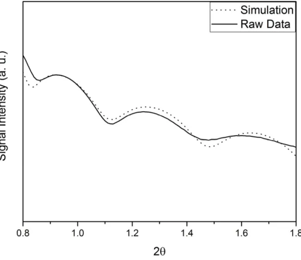
Figure S1: The experimental and software-generated XRR curves featuring Kiessig fringes
S-3