Alcohol-Based Digital Etch for III–V Vertical
Nanowires With Sub-10 nm Diameter
The MIT Faculty has made this article openly available.
Please share
how this access benefits you. Your story matters.
Citation
Lu, Wenjie et al. "Alcohol-Based Digital Etch for III–V Vertical
Nanowires With Sub-10 nm Diameter." IEEE Electron Device Letters
38, 5 (May 2017): 548 - 551 © 2017 IEEE
As Published
http://dx.doi.org/10.1109/led.2017.2690598
Publisher
Institute of Electrical and Electronics Engineers (IEEE)
Version
Author's final manuscript
Citable link
https://hdl.handle.net/1721.1/126190
Terms of Use
Creative Commons Attribution-Noncommercial-Share Alike
Abstract—This letter introduces a novel alcohol-based digital
etch technique for III-V FinFET and nanowire MOSFET fabrication. The new technique addresses the limitations of the conventional water-based approach in enabling structures with sub-10 nm 3D features. Using the same oxidation step, the new technique shows an etch rate of 1 nm/cycle, identical to the conventional approach. Sub-10 nm fins and nanowires with a high mechanical yield have been achieved. InGaAs nanowires with diameter of 5 nm and an aspect ratio > 40 have been demonstrated. The new technique has also been successfully applied to InGaSb-based heterostructures, the first demonstration of digital etch in this material system. Vertical InGaAs nanowire gate-all-around MOSFETs with a subthreshold swing of 70 mV/dec at VDS = 50 mV have been obtained at a
nanowire diameter of 40 nm, demonstrating the good interfacial quality that the new technique provides.
Index Terms— Digital etch, InGaAs, InGaSb, nanowire,
FinFETs, nanowire MOSFETs
I. INTRODUCTION
-V compound semiconductors are regarded as promising candidates to replace silicon in future generations of CMOS technology. In the quest for enhanced performance over silicon devices at advanced nodes, III-V multi-gate transistors such as FinFETs or nanowire gate-all-around MOSFETs (NW-MOSFETs) are being pursued with fin width or nanowire diameter in the sub-10 nm range. In this dimensional regime, precise etching control is paramount. Inspired by the atomic layer etching technology developed in silicon [1], [2], the concept of digital etch (DE) was introduced to III-V compound semiconductors [3]–[8]. In digital etch, the oxidation and oxide removal steps characteristic of chemical etching are performed separately. This makes them both self-limiting affording nanometer-scale control of the etching process. Digital etch has been shown to preserve high aspect ratio features, enabling precise device dimension engineering.
Manuscript received Nov. 9, 2016; revised Mar. 3, 2017; accepted Mar. 27, 2017. This work was supported by Samsung Electronics, Defense Threat Reduction Agency grant HDTRA 1-14-1-0057, NSF Center for Energy Efficient Electronics Science (award 0939514), Lam Research, and Korea Institute of Science and Technology. The review of this letter was arranged by Editor ___.
W. Lu, X. Zhao, D. Choi, and J. A. del Alamo are with the Microsystems Technology Laboratories, Massachusetts Institute of Technology, Cambridge, MA 02139, USA (e-mail: wenjie@mit.edu).
S. El Kazzi is with IMEC, 3001 Leuven, Belgium.
It has also been shown to be effective in mitigating surface damage induced by RIE [9]. In the last few years, the use of digital etch has enabled demonstrations of aggressively scaled III-V FinFETs and NW-MOSFETs with exciting electrical characteristics [10]–[14].
So far, DE has been solely applied to arsenide-based III-Vs, achieving a smallest feature size of 5 nm in fins [15] and 7 nm in lateral nanowires [10]. On the other hand, demonstrations of high aspect ratio vertical nanowires (VNW) by DE have been limited to 11-15 nm diameter [12]. This is a result of nanowire breakage as a consequence of the strong mechanical stress exerted by the water-based acids used in the oxide removal step of DE. In addition, conventional DE does not work on antimonide-based III-Vs, an important class of materials with potential for p-channel MOSFETs and tunnel-FETs [12], [16]– [18]. Antimonides are highly reactive and can be etched by water, negating the tight etching control that is sought in DE.
In this letter, we introduce a novel non-aqueous DE technique that overcomes these challenges. The new approach uses acids dissolved in alcohol which has less surface tension than water. We obtain a consistent 1 nm/cycle etching rate on both InGaAs and InGaSb-based heterostructures. We also demonstrate a 97% mechanical yield of sub-10 nm VNWs after 7 etch cycles. In addition, we show InGaAs vertical single
Alcohol-based Digital Etch for III-V Vertical
Nanowires with Sub-10 nm Diameter
Wenjie Lu, Student Member, Xin Zhao, Student Member, Dongsung Choi, Salim El Kazzi,
and Jesús A. del Alamo, Fellow, IEEE
III
Fig. 1 (a) Evolution of InGaAs VNWs in a sequential etch experiment involving different numbers of digital etch cycles in 10% HCl:IPA. (b) InGaAs VNW with 5 nm diameter, 230 nm height obtained after 10 cycles of digital etch in H2SO4:methanol. (c) 10 nm wide InGaSb fin obtained after 5
NW-MOSFETs fabricated by this technique with excellent subthreshold characteristics.
II. EXPERIMENT
DE of a III-V semiconductor consists of an oxidation step, typically performed dry in oxygen plasma [7], or wet in ozonated water [13] or H2O2 [3], [4], followed by an oxide
removal step, conventionally carried in water-based H2SO4 [3],
[9], [11] or HCl [3], [10], [12], [13]. When performed separately, both steps are self-limiting resulting in a highly controlled etch rate in the nanometer per cycle range.
We explore the use of alcohol-based acids for the oxide removal sub-cycle. The motivation is twofold. On the one hand, we seek to reduce the surface tension of the acid removal step in an effort to enhance the survivability of very thin nanowires. Secondly, we seek a DE technique for antimonides which are highly reactive and easily oxidized and etched in water. This is particularly the case if there are defects from material growth or plasma damage.
We compare three oxide removal chemistries: 4.1 M H2SO4
in DI water, 2.0 M H2SO4 in methanol, and 0.1 M HCl in
isopropanol IPA1. H2SO4 and HClare chosen as they are the
most used acids for InGaAs DE. For antimonides, only HCl-based etch is studied since antimonides are attacked by H2SO4. In all cases, oxidation is performed in oxygen plasma
for 3 min in a barrel asher. The starting arsenide heterostructure consists of multiple layers of In0.53Ga0.47Asand In0.52Al0.48As
grown by MBE on an InP substrate. The antimonide heterostructure consists of 20 nm of In0.28Ga0.62Sb on 200 nm
Al0.65Ga0.35Sb buffer, grown by MBE on a GaAs substrate.
After standard surface cleaning and native oxide removal, a 2 nm Si3N4 adhesion layer is deposited, followed by 100 nm
hydrogen silsesquioxane (HSQ). Fin and vertical nanowire
1 The solvent-based acids are commercially available at Sigma-Aldrich Co., as methanolic H2SO4 and HCl-2-proponol solution.
patterns are defined by e-beam lithography. The samples are then dry etched by BCl3/Ar/SiCl4 ICP at 250°C for 2 min [9],
resulting in a final fin or VNW height of about 230 nm. After RIE, the arsenide sample is dipped in BOE for 30 s to remove the HSQ mask and native oxide. The antimonide sample is dipped in the HCl:IPA solution for 30 s, to remove the native oxide, with the HSQ remaining. At this point, various cycles of digital etch are carried out. Between cycles, fin width and VNW diameter are measured by SEM to monitor the etch rate. Fig. 1(a) demonstrates the thinning process of an arsenide VNW with initial diameter of 34 nm, after 2, 5, and 10 DE cycles in HCl:IPA. Fig. 1(b) shows the narrowest arsenide VNW obtained with a 5 nm diameter and 230 nm height (aspect ratio = 46). Fig. 1(c) shows a 10 nm wide antimonide fin.
III. RESULTS AND DISCUSSION
Etch-rates were obtained by measuring VNW diameter by SEM on sets of 12 NWs of various initial diameters. Figs. 2(a) and (b) show the evolution of arsenide NW diameter in alcohol-based HCl and H2SO4, respectively. The average radial
etch rate in HCl:IPA is 1.0 ± 0.04 nm/cycle, and in H2SO4:methanol is 1.2 ± 0.05 nm/cycle . These values closely
match the etch rate using H2SO4:DI water which is
1.0 ± 0.1 nm/cycle.
Fig. 2(c) shows the change in an antimonide NW after dipping in DI water for 2 minutes. The diameter decreases from
Fig. 2 Evolution of arsenide VNW diameter with number of DE cycles in (a) 10% HCl:IPA; (b) 10% H2SO4:methanol; (c) Antimonide VNW and fin before
and after dipping in DI water for 2 min; (d) Antimonide VNW after dipping in HCl:IPA for 2 min; (e) Same as (a) but for antimonide VNW in 10% HCl:IPA. In (a), (b) and (e), the legends indicate the initial VNW diameter after RIE.
Fig. 3 Arsenide VNW array after 7 DE cycles in (a) 10% HCl in DI water, (b) 10% HCl in IPA, and (c) 10% H2SO4 in methanol. The insets show close ups
of the etched structures. The nanowire mechanical yield in (a) is 0%, while the one in (b) is 97% and in (c) is 90%. (d) Tightly-packed arsenide VNW array after 7 DE cycles in 10% HCl:IPA. The NW diameter is 10 nm and spacing is 80 nm.
TABLEI
MECHANICAL YIELD OF INGAAS VNWS AFTER 7 CYCLES OF DIGITAL ETCH
DIntial (nm) DFinal (nm) DE:HCl/H2O Rinse:H2O DE:HCl/IPA Rinse:IPA DE:H2SO4/methanol Rinse:IPA DE:HCl/H2O Rinse:IPA 28 14 100% 100% 100% 100% 26 12 31% 100% 100% 100% 24 10 5% 100% 100% 0% 22 8 0% 97% 95% 0% 20 6 0% 5% 90% 0%
100 nm to 92 nm. Also, the NW sidewall and AlGaSb field surface become rough and trenches appear at the heterojunction interfaces. The antimonide fin sidewall in Fig. 2(c) also reveals such etching. Therefore, water-based DE is not viable for antimonides. This issue is relieved by using alcohol-based solutions. Fig. 2(d) shows an antimonide NW after dipping in 10% HCl:IPA for 2 minutes. No excessive sidewall etching or surface damage is observed, implying that the etching is self-limited after removing the layer of oxide on the sidewall. Fig. 2(e) shows the HCl:IPA digital etch rate of antimonide NWs, exhibiting a radial etching rate of 1.0 ± 0.1 nm/cycle.
A key challenge for devices fabricated by DE is the low mechanical yield of the process in the sub-10 nm regime. This is a result of the high surface tension of water during dipping and rinsing, and is particularly problematic for VNWs which, unlike fins, cannot be anchored at both ends. Fig. 3(a) shows an arsenide VNW array (initial diameter = 22 nm) after 7 cycles of conventional DE. A final NW diameter of 8 nm is expected but all structures are destroyed. In contrast, Fig. 3(b) shows an identical sample processed side-by-side in HCl:IPA. 8 nm diameter VNWs are demonstrated with over 97% mechanical yield. Moreover, no clustering is observed for tightly spaced VNWs [19]. This is revealed in Fig. 3(d) where a 10 nm diameter VNW array spaced by 80 nm is shown.
Table 1 summarizes the mechanical yield of arsenide VNWs after 7 DE cycles with various nominal final diameters, for water as well as alcohol-based acids. The superiority of the new technique is clearly demonstrated. It should be noted that 7 DE cycles is a harsh process that is typically unnecessary in actual device fabrication. In a shortened process, higher mechanical yields at smaller diameters should be possible.
It is worth noting that, although there are other drying methods which can minimize surface tension, such as critical
point drying (CPD), a solvent-based treatment is most compatible with CMOS manufacturing. Drying methods such as CPD are often time consuming, making them infeasible when multiple cycles of DE are required. In addition, breakage of VNWs can happen both in the etching and rinsing steps. To clarify the relative contributions, Table 1 includes the mechanical yield of methanolic H2SO4 DE, and aqueous HCl
DE with IPA rinsing. Although IPA rinsing improves the mechanical yield of HCl:H2O DE drastically at D = 12 nm, it
shows no difference at and below 10 nm. Interestingly, the H2SO4:methanol DE shows much better yield at the smallest
final diameter of 6 nm than the HCl:IPA DE, even though both methods are rinsed with IPA. This is shown in Fig. 3(c). This is likely due to the smaller viscosity of methanol (0.54 cP) than that of IPA (2.0 cP). These results indicate that NW breakage happens during the oxide etch process as well as while rinsing.
IV. INGAAS NW-MOSFETS
To illustrate the practical applicability of the new DE process, we have fabricated InGaAs VNW-MOSFETs through a process similar to that of [14] using a similar heterostructure to [20]. The process includes 5 DE cycles in 4.1 M H2SO4:methanol.
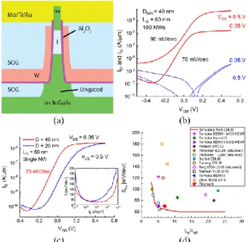
Fig. 4(a) shows a schematic cross-section of the device which features a 2 nm thick Al2O3 gate dielectric (EOT = 1 nm), W
gate metal, and Mo ohmic contacts. NW diameters range from 20 to 40 nm, the channel length is 80 nm.
The linear subthreshold characteristics of a typical device consisting of 100 NWs with 40 nm diameter is shown in Fig. 4(b). A linear subthreshold swing, Slin, of 78 mV/dec is
obtained on the NW array. As shown in Fig. 4(c), a single NW device with 40 nm diameter exhibits a minimum Slin of
70 mV/dec. The 20 nm diameter device shows a minimum S of 74 mV/dec at VDS = 0.5 V. The Dit estimated from the linear
subthreshold characteristics is approximately 3.9∙1012 eV-1cm-2.
Devices with such narrow diameters suffer from high contact resistance at low VDS due to small top contact area. The inset of
Fig. 3(c) shows that S remains below 80 mV/dec over two orders of magnitude of ID. This is one of the best linear
subthreshold swings reported in InGaAs VNW-MOSFETs, as shown in Fig. 4(d) [21]. This indicates that the new DE technique delivers sidewall quality comparable to the conventional approach.
V. CONCLUSIONS
In this work, a novel digital etch scheme utilizing alcohol-based etchants for use in III-V nanostructures is reported. The new approach exhibits excellent mechanical yield at sub-10 nm critical dimensions. Digital etch on the antimonide material system is demonstrated for the first time. Vertical nanowire InGaAs MOSFETs have been fabricated using the new technique. Subthreshold characteristics with minimum S of 70 mV/dec and 74 mV/dec are obtained on single NW MOSFET with diameters of 40 and 20 nm, respectively.
VI. ACKNOWLEDGEMENT
Device fabrication was carried out at the Microsystems Technology Laboratories and SEBL of MIT.
Fig. 4 (a) Schematic cross-section of InGaAs VNW-MOSFET; (b) subthreshold characteristics for a VNW transistor array with D = 40 nm and 100 VNWs, treated with 5 DE cycles in H2SO4:methanol; (c) subthreshold
characteristics of a single VNW transistor with D = 40 nm with lowest Slin of
70 mV/dec. The inset shows S vs. ID of this device. (d) Linear subthreshold
VII. REFERENCES
[1] K. J. Kanarik, T. Lill, E. A. Hudson, S. Sriraman, S. Tan, J. Marks, V. Vahedi, and R. A. Gottscho, “Overview of atomic layer etching in the semiconductor industry,” J. Vac. Sci. Technol. A, vol. 33, no. 2, pp. 020802.1-020802.15, Mar. 2015, DOI: 10.1116/1.4913379.
[2] J. Yamamoto, T. Kawasaki, H. Sakaue, S. Shingubara, and Y. Horiike, “Digital etching study and fabrication of fine Si lines and dots,” Thin
Solid Films, vol. 225, no. 1, pp. 124–129, Mar. 1993, DOI:
10.1016/0040-6090(93)90140-K.
[3] G. C. DeSalvo, C. A. Bozada, J. L. Ebel, D. C. Look, J. P. Barrette, C. L. A. Cerny, R. W. Dettmer, J. K. Gillespie, C. K. Havasy, T. J. Jenkins, K. Nakano, C. I. Pettiford, T. K. Quach, J. S. Sewell and G. D. Via, “Wet chemical digital etching of GaAs at room temperature,” J.
Electrochem. Soc., vol. 143, no. 11, pp. 3652–3656, Nov. 1996, DOI:
10.1149/1.1837266.
[4] A. Alian, C. Merckling, G. Brammertz, M. Meuris, M. Heyns, and K. D. Meyer, “InGaAs MOS transistors fabricated through a digital-etch gate-recess process and the influence of forming gas anneal on their electrical behavior,” ECS J. Solid State Sci. Technol., vol. 1, no. 6, pp. 310–314, Jan. 2012, DOI: 10.1149/2.001301jss.
[5] S. Lee, C.-Y. huang, D. Cohen-Elias, J. J. M. Law, V. Chobpattanna, S. Krämer, B. J. Thibeault, W. Mitchell, S. Stemmer, A. C. Gossard, and M. J. W. Rodwell, “High performance raised source/drain InAs/In0.53Ga0.47As channel metal-oxide-semiconductor field-effect-transistors with reduced leakage using a vertical spacer,”
Appl. Phys. Lett., vol. 103, no. 23, pp. 233503.1-233503.4, Dec. 2013,
DOI: 10.1063/1.4838660.
[6] S. Lee, C.-Y. Huang, A. D. Carter, J. J. M. Law, D. C. Elias, V. Chobpattana, B. J. Thibeault, W. Mitchell, S. Stemmer, A. C. Gossard, and M. J. W. Rodwell, “High transconductance surface channel In0.53Ga0.47As MOSFETs using MBE source-drain regrowth and surface digital etching,” in 2013 International Conference on Indium
Phosphide and Related Materials (IPRM), 2013, pp. 1–2, DOI:
10.1109/ICIPRM.2013.6562630.
[7] J. Lin, X. Zhao, D. A. Antoniadis, and J. A. del Alamo, “A novel digital etch technique for deeply scaled III-V MOSFETs,” IEEE Electron Device Lett., vol. 35, no. 4, pp. 440–442, Apr. 2014, DOI: 10.1109/LED.2014.2305668.
[8] C. Y. Huang, P. Choudhary, S. Lee, S. Kraemer, V. Chobpattana, B. Thibeault, W. Mitchell, S. Stemmer, A. Gossard, and M. Rodwell, “12 nm-gate-length ultrathin-body InGaAs/InAs MOSFETs with 8.3∙105
ION/IOFF,” in 2015 73rd Annual Device Research Conference (DRC), 2015, pp. 260–260, DOI: 10.1109/DRC.2015.7175669.
[9] X. Zhao and J. A. del Alamo, “Nanometer-scale vertical-sidewall reactive ion etching of InGaAs for 3-D III-V MOSFETs,” IEEE
Electron Device Lett., vol. 35, no. 5, pp. 521–523, May 2014, DOI:
10.1109/LED.2014.2313332.
[10] X. Zhou, N. Waldron, G. Boccardi, F. Sebaai, C. Merckling, G. Eneman, S. Sioncke, L. Nyns, A. Opdebeeck, J. W. Maes, Q. Xie, M. Givens, F. Tang, X. Jiang, W. Guo, B. Kunert, L. Teugels, K. Devriendt, A. Sibaja Hernandez, J. Franco, D. van Dorp, K. Barla, N. Collaert, and A. V-Y. Thean, “Scalability of InGaAs gate-all-around FET integrated on 300mm Si platform: Demonstration of channel width down to 7nm and Lg down to 36nm,” 2016 IEEE Symposium on
VLSI Technology, Honolulu, HI, 2016, pp. 1-2, DOI: 10.1109/VLSIT.2016.7573420.
[11] A. Vardi and J. A. del Alamo, “Sub-10 nm fin-width self-aligned InGaAs FinFETs,” IEEE Electron Dev. Lett., vol. 37, no. 9, pp. 1104-1107, Sept. 2016, DOI: 10.1109/LED.2016.2596764.
[12] E. Memišević, J. Svensson, M. Hellenbrand, E. Lind, and L. E. Wernersson, “Scaling of vertical InAs-GaSb nanowire tunneling field-effect transistors on Si,” IEEE Electron Device Lett., vol. 37, no. 5, pp. 549–552, May 2016, DOI: 10.1109/LED.2016.2545861. [13] N. Waldron, S. Sioncke, J. Franco, L. Nyns, A. Vais, X. Zhou, H. C.
Lin, G. Boccardi, J. W. Maes, Q. Xie, M. Givens, F. Tang, X. Jiang, E. Chiu, A. Opdebeeck, C. Merckling, F. Sebaai, D. van Dorp, L. Teugels, A. Sibaja Hernandez, K. De Meyer, K. Barla, N. Collaert, and Y-V. Thean, “Gate-all-around InGaAs nanowire FETS with peak transconductance of 2200uS/um at 50nm Lg using a replacement fin RMG flow,” 2015 IEEE Int. Electron Dev. Meeting, Washington, DC 2015, p. 31.1.1-31.1.4, DOI: 10.1109/IEDM.2015.7409805.
[14] X. Zhao, A. Vardi, and J. A. del Alamo, “InGaAs/InAs heterojunction vertical nanowire tunnel FETs fabricated by a top-down approach,”
2014 IEEE Int. Electron Dev. Meeting, San Francisco, CA, 2014, pp.
25.5.1-25.5.4, DOI: 10.1109/IEDM.2014.7047108.
[15] A. Vardi, X. Zhao, and J. A. del Alamo, “Quantum-size effects in sub 10-nm fin width InGaAs FinFETs,” in 2015 IEEE Int. Electron Dev.
Meeting, Washington, DC, 2015, pp. 31.3.1-31.3.4, DOI: 10.1109/IEDM.2015.7409807.
[16] A. Nainani, T. Irisawa, Z. Yuan, Y. Sun, T. Krishnamohan, M. Reason, B. R. Bennett, J. B. Boos, M. G. Ancona, Y. Nishi, and K. C. Saraswat, “Development of high-k dielectric for antimonides and a sub 350 C III-V pMOSFET outperforming germanium,” 2010 IEEE Int. Electron
Dev. Meeting, San Francisco, CA, 2010, pp. 6.4.1-6.4.4, DOI:
10.1109/IEDM.2010.5703309.
[17] W. Lu, J. K. Kim, J. F. Klem, S. D. Hawkins, and J. A. del Alamo, “An InGaSb p-channel FinFET,” 2015 IEEE Int. Electron Dev. Meeting, Washington, DC, 2015, pp. 31.6.1-31.6.4, DOI: 10.1109/IEDM.2015.7409810.
[18] Q. Smets, A. S. Verhulst, S. El Kazzi, D. Gundlach, C. A. Richter, A. Mocuta, N. Collaert, A. V-Y. Thean, and M. M. Heyns, “Calibration of the effective tunneling bandgap in GaAsSb/InGaAs for improved TFET performance prediction,” IEEE Trans. on Electron Devices, vol. 63, no. 11, pp. 4248–4254, Nov. 2016, DOI: 10.1109/TED.2016.2604860.
[19] C. Thelander, C. Rehnstedt, L. E. Fröberg, E. Lind, T. Mårtensson, P. Caroff, T. Löwgren, B. J. Ohlsson, L. Samuelson, and L-E. Wernersson, "Development of a vertical wrap-gated InAs FET," IEEE
Trans. on Electron Devices, vol. 55, no. 11, pp. 3030- 3036, Nov. 2008,
DOI: 10.1109/TED.2008.2005151.
[20] X. Zhao, J. Lin, C. Heidelberger, E. A. Fitzgerald, and J. A. del Alamo, “Vertical nanowire InGaAs MOSFETs fabricated by a top-down approach,” 2013 IEEE Int. Electron Dev. Meeting, 2013, pp. 28.4.1-28.4.4, DOI: 10.1109/IEDM.2013.6724710.
[21] J. A. del Alamo, D. A. Antoniadis, J. Lin, W. Lu, A. Vardi, and X. Zhao, “Nanometer-scale III-V MOSFETs,” IEEE Journal of the
Electron Device Society, vol. 4, no. 5, pp. 205-214, Sept. 2016, DOI: