Chemical Vapor Deposition of Organosilicon and
Sacrificial Polymer Thin Films
by
Thomas Bryan Casserly
B.S. in Chemical Engineering
Texas A&M University, 1999
Submitted to the Department of Chemical Engineering in Partial Fulfillment of the Requirements for the Degree of
DOCTOR OF PHILOSOPHY IN CHEMICAL ENGINEERING
AT THE
MASSACHUSETTS INSTITUTE OF TECHNOLOGY
June 2005
©
2005 Massachusetts Institute of Technology. All rights reserved.
Signature
of Author
...
... ...
Department of Cemical Enering
May 13, 2005Certified by .. ...
... ... ...
Karen K. Gleason
Professor of Chemical Engineering
Thesis Supervisor
Accepted by ...
...
... ...
Daniel Blankschtein
PrFnfr nF (-h4 m
,al
l-nrioo riirMASSACHUSETTS INST/E
OF TECHNOLOGY
JUN 01 2005
Chemical Vapor Deposition of Organosilicon and
Sacrificial Polymer Thin Films
By
Thomas Bryan Casserly
Submitted to the Department of Chemical Engineering
on May 13, 2005 in Partial Fulfillment of the
Requirements for the Degree of
Doctor of Philosophy in Chemical Engineering
ABSTRACT
Chemical vapor deposition (CVD) produced films for a wide array of
applications from a variety of organosilicon and organic precursors. The
structure and properties of thin films were controlled by varying
processing conditions such as the method and power of precursor
activation, pressure, flow rates, and substrate temperature. Systematic
variance of deposition conditions allows for the design of materials for a
specific application, highlighting the versatility of CVD processes.
Spectroscopic tools including Fourier transform infrared spectroscopy,
variable
angle
spectroscopic
ellipsometry,
X-ray photoelectron
spectroscopy, Raman spectroscopy, and nuclear magnetic resonance
(NMR) spectroscopy were utilized to characterize film structure and
understand the relationship between the structure and properties of
materials. Computational quantum mechanics is a power tool applied to
explain observed phenomena such as unreferenced chemical shifts in the
29Si
NMR of organosilicon
thin films, and to examine the
thermochemistry of a family of methyl- and methoxymethylsilanes
enabling the prediction of initial reactions occurring in the CVD process.
Thesis Supervisor: Karen K. Gleason
Title: Professor of Chemical Engineering
To Mom and Dad
&
ACKNOWLEDGEMENTS
While many applaud the accomplishment that is the conclusion of my graduate career at MIT, the praise is most often misplaced. I accomplish nothing on my own merit but what is made possible by Christ. I owe a great deal of thanks to countless individuals for their thoughts, prayers, support, friendship, generosity and advice which carried me to this end.
To my advisor, Karen, for always pushing the right buttons leading me and guiding me and fostering my maturation as a writer and scientist, I am eternally grateful. You expect the best of me and your encouragement even in the face of my greatest challenges provided the drive to succeed for you, myself and everyone counting on me and supporting me.
To my thesis committee members, Professors Herb Sawin and Bernhardt Trout, who generously gave of their time, talent and expertise while always encouraging me to pursue and develop new ideas.
On this journey, I have been blessed to work with some truly exceptional individuals. Many thanks to the members of the Gleason group, past and present, I am proud to have shared time with each of you. Ken, your knowledge, kindness, generosity and heart are without rival. Dan, your inspired leadership of "team low-k" even in the face your own self deprecating humorous pessimism rang true to the great teacher and researcher that you are. April, your smile and grace made the long hours in lab and interminable conference sessions enjoyable.
Kelvin, I am honored to have worked with such a brilliant and generous researcher and you will always be "the man."
To all the individuals who played alongside me on the intramural fields, I will always look back fondly on the memories made and championships won. I am especially grateful to the fourteen other members of the victorious CHEME Octathon team that won in my final year after four runner up finishes. I must also thank all the department degenerates whose money I have taken and who more often have taken my money at the table. You gentlemen of the fields and tables provided many a night of camaraderie that will surely be missed. To Paul, who I shared not only the field and the table with but also the first year offices, thanks for your humor, generosity and lasting friendship and for helping Holly with her accent.
To my sisters, Colleen and Amanda, who will never let my head get to big and have been a constant well of support, prayers, and entertainment, I thank you and love you and families dearly.
To my loving, caring, supportive parents, who have always believed in me and instilled in me the desire to always learn something new and make new discoveries, you have given me the greatest gift, a perfect example of a loving family. You have taught me to love selflessly, give freely, and dream beyond my imagination. No words can ever express the depth of my gratitude and love.
Finally to my bride, Holly, there are not words in any language that can describe how I feel about you. You have given so freely of yourself, supported our family, met my every need, showed me how it was done by beating me to graduation with your commencement at Harvard, and provided the motivation to finally graduate. There is no way that I would have made it to this point without you. To my baby Catherine, you are my pride and joy and I love you with all of my heart. Without your smile or Daddy playtime or especially your naps with Daddy, the final push to graduation would have been unbearable. Thank you all.
LIST OF ACRONYMS, ABBREVIATIONS, AND SYMBOLS
Bond angle between atoms listed Average Connectivity Number
Methylsilane Dimethoxydimethylsilane Dimethylsilane Trimethoxymethylsilane Trimethylsilane Tetramethoxysilane Tetramethylsilane
Atomic Force Microscopy Asymmetric stretching mode Bond dissociation energies Capacitance
Chemical Mechanical Polishing Cross-polarization
Continuous Set of Gauge Transformations Chemical Vapor Deposition
Continuous Wave
Di-oxygen substituted (CH3)2SiO2
Dimethylsilanone
Tetramethylcyclodisiloxane Hexamethylcyclotrisiloxane Octamethylcyclotetrasiloxane Density functional theory Total Energy
Mass Flow
Fourier Transform Infrared Spectroscopy Gaussian 2 theory for calculating heats of formation
Gauge-Independent Atomic Orbital Hot filament Chemical Vapor Deposition Individual Gauges for Atoms In Molecules Interlayer dielectric
Inter-metal dielectric
Interferometry for Thermal Stability Dielectric Constant
Length
Mono-oxygen substituted (CH3)3SiO
Molecular Weight Magic angle spinning
Methyl (CH3) Methylmethacrylate Methoxytrimethylsilane Methylsilsesquioxane zXYZ <r> iMS 2MO2MS 2MS 3MOMS 3MS 4MOS 4MS AFM ASM BDE C CMP CP CSGT CVD CW D D1 D2 D3 D4 DFT E FM FTIR G2 GIAO HFCVD IGAIM ILD IMD ITS k L M M, MW MAS Me MMA MO3MS MSQ
n Index of Refraction
n63 3 Index of refraction at 633 nm
NMR Nuclear magnetic resonance
NSF National Science Foundation
oRn Organically substituted n unit siloxane ring bound to film structure
OSG Organosilicate Glass
P
Pitch
P Pressure
PDMS Polydimethylsiloxane
PECVD Plasma-Enhanced Chemical Vapor Deposition
PMMA Polymethylmethacrylate
PNB Polynorbornene
PP Pulsed plasma
PPECVD Pulsed Plasma-Enhanced Chemical Vapor Deposition
ppm Parts per million
PTFE Polytetrafluoroethylene
Q
Quad-oxygen substituted SiO4r Deposition Rate
R Gas Constant
R Resistance
RF Radio Frequency
scem Standard Cubic Centimeters per Minute
SIA Semiconductor Industry Association
SiCOH Organosiloxane / Carbon Doped Oxide
SRC Semiconductor Research Corporation
SSM Symmetric stretching mode
T Temperature
T Tri-oxygen substituted (CH3)SiO3
Tf Filament Temperature
Ti Thickness of layer i
TMS Tetramethylsilane
VASE Variable Angle Spectroscopic Ellipsometry
XPS X-Ray photoelectron spectroscopy
ZPE Zero-point energy
y Vibrational rocking mode
6 Vibrational bending mode
LAG°rxn Standard Gibbs Free Energy of Reaction
AH°f or rxn Standard Enthalpy of Formation or Reaction
co Vacuum Permittivity
v Vibrational stretching mode
p Metal resistivity
YDo Sum of the atomization energies
TABLE OF CONTENTS
ABSTRACT ... 2
DEDICATION ... 3
ACKNOWLEDGEMENTS
...
4
LIST OF ACRONYMS, ABBREVIATIONS, AND SYMBOLS ... 5
LIST OF FIGURES ... 11
LIST OF TABLES ... 14
CHAPTER ONE
INTRODUCTION ... 161.1 MOTIVATION ... 17
1.2 LOW-K MATERIAL OPTIONS AND APPROACHES ... 19
1.3 CHEMICAL VAPOR DEPOSITION ... 23
1.4 COMPUTATIONAL QUANTUM MECHANICS ... 25
1.5 THESIS FRAMEWORK ... 26
REFERENCES ... 28
CHAPTER
Two
HOT-FILAMENT CHEMICAL VAPOR DEPOSITION OF ORGANOSILICON THIN FILMS FROM HEXAMETHYLCYCLOTRISILOXANE AND OCTAMETHYLCYCLOTETRASILOXANE ... 29ABSTRACT ... 30
2.1 INTRODUCTION ... 31
2.2 EXPERIMENTAL ... 32
2.3 RESULTS AND DISCUSSION ... 34
2.3.1
Deposition Rate ...
34
2.3.3
Raman Spectroscopy ...
41
2.3.4
Nuclear Magnetic Resonance (NMR) Spectroscopy ...
47
2.3.5
X-Ray Photoelectron Spectroscopy (XPS) ...
51
2.3.6
Atomic Force Microscopy (AFM) ...
52
2.3.7
Chemical Reactions ...
53
2.3.8
Film Structure ...
59
2.4 CONCLUSIONS ... 61
REFERENCES ... 62
CHAPTER THREE
DENSITY FUNCTIONAL THEORY CALCULATION OF 29SI NMR CHEMICAL SHIFTS OF ORGANOSILOXANES ... 64ABSTRACT ... 65
3.1 INTRODUCTION ... 66
3.2 METHODOLOGY AND EXPERIMENTS ... 69
3.3 RESULTS AND DISCUSSION ... 72
3.4 CONCLUSIONS ...81
REFERENCES ... 83
CHAPTER FOUR
ENTHALPIES OF FORMATION AND REACTION FOR PRIMARY REACTIONS OF METHYL- AND METHOXYMETHYLSILANES FROMDENSITY FUNCTIONAL
THEORY ...
...
85
ABSTRACT ... 86
4.1 INTRODUCTION ... 87
4.2 COMPUTATIONAL METHOD ... 89
4.3 RESULTS AND DISCUSSION ... 92
4.3.1 Enthalpies
of Formation
...
92
4.3.2
Reaction Enthalpies and Bond Dissociation Energies ...97
REFERENCES
...
107
CHAPTER FIVE
CHEMICAL VAPOR DEPOSITION OF ORGANOSILICON THIN FILMSFROM METHOXYMETHYLSILANES
.
...
ABSTRACT ... 1105.1 INTRODUCTION ... 111
5.2 RESULTS AND DISCUSSION ... 112
5.2.1. Fourier Transform Infrared (FTIR) Spectroscopy ... 112
5.2.2.
Optical and Electrical Characterization
...
1225.2.3. Interpreting the results in light of
DFT
simulations ...124
5.3 CONCLUSIONS ... 126
5.4 EXPERIMENTAL ... 127
REFERENCES... 130
CHAPTER SIX
EFFECT OF SUBSTRATE TEMPERATURE ON THE PLASMA POLYMERIZATION OF POLY(METHYL MEHTACRYLATE) ... ... 131ABSTRACT ... 132
6.1 INTRODUCTION ... 133
6.2 RESULTS AND DISCUSSION ... 134
6.2.1
Fourier Transform Infrared (FTIR) Spectroscopy to determine
optimal W/FM ...
134
6.2.2
Thermal properties/degradation of PMMA ...
137
6.2.3
X-Ray Photoelectron Spectroscopy (XPS) ...
142
6.2.4
Raman Spectroscopy ...
146
6.2.5
Deposition Kinetics ...
151
6.3 CONCLUSIONS ... 152
6.4 EXPERIMENTAL ... 153
CHAPTER SEVEN
CONCLUSIONS AND FUTURE DIRECTIONS ... 158
7.1 CONCLUSIONS ... ... 159
7.1.1 CVD Materials...159
7.1.2 Computational Quantum Mechanics ... 161
LIST OF FIGURES
CHAPTER ONE
FIGURE 1-1. PROGRESSION OF THE SIA TECHNOLOGY ROADMAP FOR DIELECTRICS ... 18
FIGURE 1-2. PROCESS FLOW FOR SIMPLE AIR GAP FABRICATION ... 21
FIGURE 1-3. SCHEMATIC OF A TYPICAL PECVD VACUUM REACTOR ... 25
CHAPTER TWO
FIGURE 2-1. FIGURE 2-2. FIGURE 2-3. FIGURE 2-4. FIGURE 2-5. FIGURE 2-6. FIGURE 2-7. FIGURE 2-8. FIGURE 2-9. FIGURE 2-10.ARRHENIUS PLOT OF D3 AND D4 FILMS PRODUCED BY HFCVD. MEASURED DEPOSITION RATES, R (LEFT AXIS), ARE DENOTED BY SOLID MARKERS, AND
THICKNESS-BASED DEPOSITION YIELDS, R/FM (RIGHT AXIS), ARE DENOTED BY
EMPTY MARKERS. STRAIGHT LINES WERE FIITED TO THE DEPOSITION YIELD DATA
BY REGRESSION ... 35 FTIR SPECTRA OF A. D3 PECVD FILM DEPOSITED UNDER CONTINUOUS-WAVE
EXCITATION AND B. D3 HFCVD FILM DEPOSITED AT 10000C ... 37
FTIR SPECTRA OF D3 HFCVD FILMS DEPOSITED AT FILAMENT TEMPERATURES OF A. 8600C, B. 10000°C, AND C. 1100o C ... 38
FTIR SPECTRA OF D4 HFCVD FILMS DEPOSITED AT FILAMENT TEMPERATURES OF
A. 8000C, B. 9000C, AND C. 10000C ... 39
MICRO-RAMAN SPECTRA OF A. D3, B. D4, C. PDMS, D. D4 HFCVD FILM DEPOSITED AT A FILAMENT TEMPERATURE OF 10000C, AND E. D3 HFCVD FILM
DEPOSITED AT A FILAMENT TEMPERATURE OF 11000C ... 42
MICRO-RAMAN SPECTRA OF D3 HFCVD FILMS DEPOSITED AT FILAMENT
TEMPERATURES OF 8600ooC, 10000°C, AND 1100°C ... 46
MICRO-RAMAN SPECTRA OF D4 HFCVD FILMS DEPOSITED AT FILAMENT
TEMPERATURES OF 800oC, 9000C, AND 10000Cloooo ... 46 29SI SOLID-STATE CP-MAS NMR SPECTRA OF D3 HFCVD FILM DEPOSITED AT FILAMENT TEMPERATURES OF 860°C, 1000C, AND 11000C ... 48 29SI SOLID-STATE CP-MAS NMR SPECTRA OF D4 HFCVD FILM DEPOSITED AT FILAMENT TEMPERATURES OF 800ooC, 9000°C, AND 10000C ... 49
ATOMIC FORCE MICROGRAPH OF D4 HFCVD FILM DEPOSITED AT A FILAMENT TEMPERATURE OF 9000C. RMS ROUGHNESS OVER IMAGE AREA IS 1.1 NM. RMS
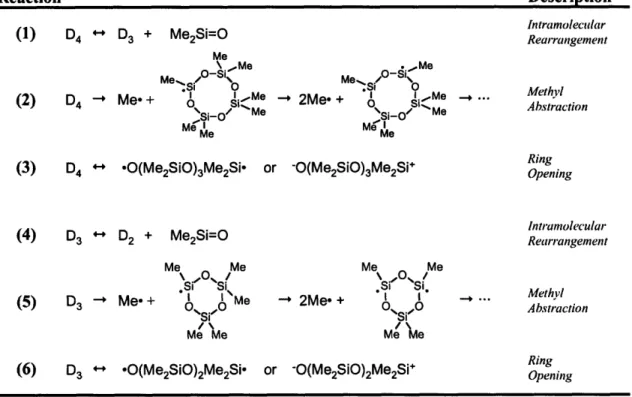
FIGURE 2-11. REACTION PATHWAYS FOR THE PRODUCTION OF POLYMERIZATION PRECURSOR SPECIES IN D3 AND D4 HFCVD ... 54
CHAPTER THREE
FIGURE 3-1. FIGURE 3-2. FIGURE 3-3. FIGURE 3-4. FIGURE 3-5. FIGURE 3-6.NON-BRANCHING GROUPS, M (+6 PPM) & D (-22PPM) AND BRANCHING GROUPS, T
(-68 PPM) & Q (-105 PPM) COMMONLY FOUND IN OSG THIN FILMS WITH 29SI
CHEMICAL SHIFTS IN ( ) ... 68
LABELED 29SI NMR SPECTRA OF HFCVD FILM FROM D3 WITH A FILAMENT
TEMPERATURE OF 1150°C ... 68
OSG GROUPS SIMULATED: A. SIH 3CAPPED D, B. D GROUPS WITH MH ENDGROUPS,
C. TWO D3* RINGS BONDED VIA SI-SI, D. D3* PENDANT TO LINEAR CHAIN OF 3 D UNITS VIA SI-SI, E. D3* PENDANT TO LINEAR CHAIN OF 3 D UNITS VIA SI-O, AND F.
D3* TERMINAL TO LINEAR CHAIN OF TWO D UNITS VIA SI-O. (D3* METHYL
ABSTRACTED D3) ... 72 29SI NMR OF HFCVD FILMS FROM D3 WITH FILAMENT TEMPERATURES OF
86o0 C, 1ooo0 C, & 110oo0 C. 11... 78
29SI NMR OF HFCVD FILMS FROM D4 WITH FILAMENT TEMPERATURES OF
8000C, 9000 C, & 1000C. 11 ... 79 29SI NMR SPECTRA OF 1150°C D3 FILM FIT TO RESOLVE CHEMICAL SHIFTS AT -8.5
PPM, -14.5 PPM AND -19.1 PPM ... 80
CHAPTER FOUR
FIGURE 4-1. FIGURE 4-2. FIGURE 4-3. FIGURE 4-4.FAMILY PLOT FOR METHOXYMETHYLSILANES - A. (CH3)NSI(OCH 3)-N, B.4
(CH3)NSIOH(OCH 3)-N, C. (CH3 3)NSIH(OCH 3-N, D. (CH)3 3)NSIH2(OCH3)2-N, E.
(CH3)NSIO-(OCH3)3-N, AND F. (CH3)NSI-(OCH 3) 3-N ... 96
FAMILY PLOT FOR METHYLSILANES - A. (CH3)NSIH4-N, B. (CH3)NSI-H3_N, C.
(CH3)NSI-..H2-N ('A1), AND D. (CH 3)NSI.H 2-N (3B1) ... 97
BDES FOR METHYLSILANES AND METHYLSILYL RADICALS AS A FUNCTION OF
METHYL SUBSTITUTION (N) ... 99
BDES FOR THE SI-C, SI-O, AND O-C BONDS FOR METHOXYMETHYLSILANES AS A
CHAPTER FIVEE FIGURE 5-1. FIGURE 5-2. FIGURE 5-3. FIGURE 5-4. FIGURE 5-5.
FTIR SPECTRA OF PECVD THIN FILMS DEPOSITED FROM MO3MS, 2MO2MS,
AND 3MOMS WITH INSET FOCUSED ON M, D, T REGION FROM 1300-1240 CM-1.
... ... ... ... ... ... ... .. ... ... 113 FTIR SPECTRA OF PECVD THIN FILMS FROM 2MO2MS, 2MO2MS + H2, AND
2MO2MS + 02 WITH AN ADDITIONAL (- - -) SPECTRUM OF THE 2MO2MS + 02
FILM AFTER ANNEAL ... 117
FTIR SPECTRA OF PECVD FILMS DEPOSITED FROM 3MOMS AND HYDROGEN WITH 3MOMS:H 2GAS FLOW RATIOS OF 1:1.5, 1:4 AND 1:8... 120
FTIR SPECTRA OF FILMS DEPOSITED FROM 3MOMS, 3MOMS + H2, AND 3MOMS
+ 02 AT PLASMA POWERS OF 20W (BLACK LINES), 40W (MEDIUM GRAY LINES), AND 100W (LIGHT GRAY LINES) ... 122
DIELECTRIC CONSTANT OF PECVD FILMS FROM METHOXYMETHYLSILANES, WITH
HYDROGEN, AND WITH OXYGEN FOR THE AS DEPOSITED SAMPLES AND AFTER
ANNEALING AS A FUCNTION OF THE INDEX OF REFRACTION AT A WAVELENGTH OF
633 NM ... 123
CHAPTER SIX
FIGURE 6-1. FIGURE 6-2. FIGURE 6-3. FIGURE 6-4. FIGURE 6-5. FIGURE 6-6. FIGURE 6-7. FIGURE 6-8.FTIR SPECTRA OF PECVD THIN FILMS FROM MMA WITH W/FM OF (A) 168.3, (B)
84.2, (C) 67.3, AND (D) 4.8 J/G ALONG WITH A (E) PMMA STANDARD ... 135
ONSET OF THERMAL DECOMPOSITION AS A FUNCTION OF SUBSTRATE
TEMPERATURE FOR BOTH CW AND PP CVD PMMA FILMS ... 140
PERCENT RESIDUE REMAINING AFTER ANNEAL AS A FUNCTION OF SUBSTRATE
TEMPERATURE FOR BOTH CW AND PP CVD PMMA FILMS ... 141
FIT XPS SPECTRA, C 1S AND O 1S FOR THE PMMA STANDARD AND THE PECVD
FILM CW 1 ... 143
PMMA WITH LABELED CARBON (1-4) AND OXYGEN (1*-2*) MOIETIES ... 144
RAMAN SPECTRA OF FILMS PP4, CW4, PP1, CW1, AND A PMMA STANDARD
(STD.) ... 149
DETAIL OF THE RAMAN SPECTRA OF FILMS PP4, CW4, PP1, CW1, AND A PMMA
STANDARD AT THE METHOXY AND SKELETAL STRETCHING REGION ... 150 ARRHENIUS PLOT OF DEPOSITION RATE AS A FUNCTION OF SUBSTRATE
TEMPERATURE AT CONSTANT W/FM = 4.8 J/G SHOWING RELATIVE APPARENT
LIST OF TABLES
CHAPTER TWO
TABLE 2-1. FTIR ASSIGNMENTS FROM THE LITERATURE ... 37
TABLE 2-2. RAMAN ASSIGNMENTS FROM THE LITERATURE ... 43 TABLE 2-3. RAMAN SILOXANE SYMMETRIC STRETCHING MODE (SSM) ASSIGNMENTS ... 45
TABLE 2-4. 29SI NMR STRUCTURES AND CHEMICAL SHIFTS COMMONLY OBSERVED IN OSG
CVD FILMS ... 48 TABLE 2-5. XPS ELEMENTAL RATIOS FOR HFCVD FILMS FROM D3 AND D4. ... 51
CHAPTER THREE
TABLE 3-1. SUMMARY OF CALCULATED 29SI NMR CHEMICAL SHIFTS OF KNOWN MOIETIES
USING VARIOUS METHODS AT THE B3LYP/6-311++G(D,P) LEVEL. (TMS aoso
GIAO: 339.2 PPM, IGAIM: 338.0 PPM, CSGT: 338.0 PPM) ... 73
TABLE 3-2. SUMMARY OF CALCULATED 29SI NMR CHEMICAL SHIFTS OF UNKNOWN MOIETIES
USING VARIOUS METHODS AT THE B3LYP/6-311++G(D,P) LEVEL. (TMS aso
GIAO: 339.2 PPM, IGAIM: 338.0 PPM, CSGT: 338.0 PPM) ... 75
CHAPTER FOUR
TABLE 4-1. TOTAL ENERGIES AND UN-SCALED ZERO-POINT ENERGIES, IN HARTREE, WITH
THERMAL CORRECTIONS TO ENTHALPY, SUM OF ATOMIZATION ENERGIES AND
ENTHALPIES OF FORMATION (BOTH THEORY AND EXPERIMENTAL WITH
DEVIATIONS), IN KCAL/MOL .. ... 94
TABLE 4-2. BOND DISSOCIATION ENERGIES FOR METHYLSILANES AND METHYLSILYL
RADICALS ... .... ... ... 98...
TABLE 4-3. BOND DISSOCIATION ENERGIES FOR METHOXYMETHYLSILANES ... 100
TABLE 4-4. GIBBS FREE ENERGY OF REACTION AND ENTHALPY OF REACTION AT 298 K AND 1
ATM FOR A SERIES OF REACTIONS OF METHYLSILANES WITH OXYGEN AND
METHOXYMETHYLSILANES WITH OXYGEN AND WITH HYDROGEN ... 103
CHAPTER FIVE
FTIR ASSIGNMENTS FOR PMMA FROM THE LITERATURE2 0 ... 137 SUMMARY OF ONSET OF THERMAL DECOMPOSITION AND % RESIDUE FOR PECVD
FILMS DEPOSITED AT VARIOUS SUBSTRATE TEMPERATURES WITH A CONSTANT W /FM OF 4.8 J/G ... 138
COMPARISON OF XPS SPECTRA FITS FROM FIGURE 6-4 WITH REFERENCE DATA.
... 144
ELEMENTAL ANALYSIS AND C/O RATIO FROM XPS SCANS ALONG WITH
CALCULATED UPPER AND LOWER BOUNDS FOR FUNCTIONAL GROUP LOSS ... 146
RAMAN ASSIGNMENTS FROM THE LITERATURE.1 0, 40 ... 148
CHAPTER SIX
TABLE 6-1. TABLE 6-2. TABLE 6-3. TABLE 6-4. TABLE 6-5.CHAPTER ONE
1.1 MOTIVATION
As the semiconductor industry continues to decrease device feature size, processor clock speeds are increasingly limited by the resistance-capacitance (RC) delay of interconnect structures.' Advances in lithography have enabled semiconductor manufacturers to decrease device size allowing for shorter, thinner, and more densely packed metal interconnects. For instances in which each level of a dielectric, metal, dielectric stack are of equal thickness, the RC delay can be expressed as:'
RC =2pKo(4L2 + L2
where
p is the metal resistivity
K is the dielectric constant of the material between the metal lines co is the permittivity of space
L is the line length P is the metal pitch
T is the thickness of the metal line
As is evident in Equation 1-1, as the wire density increases, indicated by a decrease in pitch (P), RC delay increases. There are two approaches to this problem from a materials standpoint. Semiconductor companies have implemented the use of copper in place of aluminum at the 0.13 micron process node to take advantage its lower resistivity.l The other is to lower the dielectric constant of the insulating film. The introduction of copper is a logical first step to reduce the RC delay; however, the
RC delay will continue to increase for future process nodes if the dielectric constant remains unchanged. Reducing the dielectric constant not only reduces the RC delay, but has the added benefit of reducing power consumption and line-to-line crosstalk noise as well. Therefore, there is a need for and a large field of research dedicated to developing low-k materials for future process nodes.
4.0 3.5
3.0
I
2.5
1
2.0 ,e pa10i
- ?I
[ * SIA Roadmap 99SIA Roadmap 010.05 0.07 0.10 0.13 0.18 0.25Upm
2011 2008 2005 2002 1999 1997
Figure 1-1. Progression of the SIA Technology Roadmap for Dielectrics.
The Semiconductor Industry Association (SIA) technology roadmap for dielectrics outlines the dielectric constant requirements for the next ten years and is updated regularly. From Figure 1-1 it can be seen that the implementation of low-k materials has been repeatedly pushed back. The most recent roadmap pushed integration of low-k films back even further, calling for a dielectric constant below 3.0 for the first time in 2007. This is due to the inability of the industry to develop and integrate a single choice for the next generation low-k material. Silicon dioxide (SiO2) is an excellent dielectric material due to its excellent mechanical and thermal
properties and has been the industry standard from the beginning. However, SiO
2-i
I
-: SIA Roadmap 97
* SIA Roadmap Update 98
* J. Ryan, SSDM, Sept 98 - --f I.! I l l~ l, . . _ . . _ . .v_
has a dielectric constant of approximately 4.0, which is too high for future devices. The current industry standard for low-k dielectrics is a fluorine-doped oxide (SiOF, 3.3 < K <3.7). Companies and researchers have developed a variety of CVD organosilicate glasses (OSG, 2.7 < K <3.3) for use as the next low-k material such as
Black DiamondTM from AMD, FlowfillT M from Trikon, and CORALTM
from Novellus.2
Companies have also developed spin-on OSGs, such as Dow's SILKTM and AlliedSignal's Accuspin 418TM. Each of these products still face many challenges before wide spread implementation. Further down the dielectric roadmap fluorocarbons (2.0 < K < 2.7) and other polymers have been proposed. While these materials all have dielectric constants lower than that of SiO2, they also create many
challenges for integration due to issues concerning thermal and dimensional stability, chemical and mechanical polishing (CMP) stability, as well as the complexity of integrating an entirely new material into the fabrication process.3
1.2 Low-K MATERIAL OPTIONS AND APPROACHES
Dielectric requirements for the sub-o.1 micron process node indicate a dielectric constant less than 2.0 (see Figure 1-1). Air has the lowest dielectric constant of -. o. Incorporating void space in the form of pores into current low-k films will enable a reduction of the dielectric constant below 2.0. Creating a porous
low-k material typically utilizes a porogen, which is removed following deposition by a thermal annealing or UV radiation step. Kohl et al.4 demonstrated this idea by spin coating a 80/20 mixture of a commercially available spin-on dielectric composed of methyl silsesquioxane (MSQ, k = 2.7) and a sacrificial polymer,
substituted polynorbornene (PNB) containing cross-linking groups. After spin coating and soft bake below the decomposition temperature of PNB, the MSQ/PNB film was heated to 425°C thermally decomposing the PNB leaving a porous MSQ film with a measured dielectric constant of 2.3. While porous films have the desired effect of reducing the dielectric constant of the remaining material, the mechanical and heat transfer properties of the film are adversely affected. The mechanical strength of porous films scales with porosity, p, by (1-p)3 while the thermal conductivity scales by (1-p)1.5.5
Most porous films lack the mechanical strength required for integration into current semiconductor manufacturing. Due to poor mechanical strength porous films may collapse or otherwise fail during various fabrication steps and affect the surrounding structures decreasing yield and increasing cost. Due to the uncertainty involved in using porous films, some researchers have investigated the possibility of using air as a dielectric.3 6, 7 While air does not have the thermal conductivity or
mechanical strength of other dielectrics, it does have the lowest possible dielectric constant, 1.0, and is the only choice for the ultimate low-k material. By using air as a dielectric, concerns about inhomogeneous pore structure causing device failure are eliminated. While the mechanical and thermal conductivity of air leaves much to be desired, the sacrificial material chosen can be a robust material providing mechanical strength and dimensional stability during critical fabrication steps eliminating risks and uncertainties associated with porous low-k materials.
The first logical step of integration of air as a dielectric is in the form of air gaps. Air gaps can be created in one of two ways. The first is to deposit a non-conformal dielectric layer on top of a patterned surface.8, 9 This technique has many
challenges. This process can only be used with metals that can be etched (which excludes copper interconnects) or requires removal of the inter-metal dielectric (IMD) via a challenging etch step. Another challenge is reproducibility of air gaps across structures of varying dimensions and non-ideal air gap geometries which often require multiple steps to ensure the dielectric overcoat does not fail. An alternative process is to deposit and pattern sacrificial layer, followed by metal deposition and etch back. The stack is then capped with a dielectric overcoat. Finally, the sacrificial layer is removed by a thermal annealing step. In a process using a sacrificial layer it is important to remove all of the sacrificial material. Any remaining residue will raise the dielectric constant and may have negative interactions with the final device. It is therefore very important to understand the decomposition mechanism, diffusion of the sacrificial material through the overlying inter-layer dielectric (ILD), and the completeness of removal.
Sacrificial Material DepositionI
Photolithography
Pattern transfer via RIE
Photoresist Strip SiO2 Deposition
Sacrificial Material Decomposition
_--Figure 1-2. Process flow for simple air gap fabrication.
Fabrication techniques for closed cavity void space using sacrificial materials have been proposed by Anand et al.6and Kohl
et
al.3, 7 The methods effectively differThe process of Anand et al. utilized magnetron sputtered amorphous carbon as a sacrificial material. The carbon was patterned to create trenches for metal deposition. Tungsten was deposited via blanket-CVD over a barrier layer of titanium nitride followed by an etchback. Silicon dioxide was then sputter-deposited capping the carbon and tungsten. The stack was then placed in an oxygen ambient furnace at 450o°C for 2 hr which ashed the amorphous carbon leaving behind air gap structures. The effective dielectric constant of the air gaps was measured to be 1.01. While
successful in creating air gap structures, the high-temperature annealing step in an oxygen environment would cause copper oxidation increasing the interconnect resistivity.
Kohl et al.3, 7 propose a similar process using spin-on deposited functionalized polynorbornene (PNB) as the sacrificial material. The PNB polymer used was heated at a rate of 3C/min under constant nitrogen purge. TGA shows decomposition occurring between 370°C and 425C. This process included etching holes in the overcoat material to prevent overcoat damage during SL removal, and approximately 3% of the polymer remained as residue negatively impacting the dielectric properties of the air gap structure. For both process, the elevated temperatures for extended annealing times may cause undesired changes in dopant profiles. The use of a CVD sacrificial material is preferred over a spin-coated material because the latter produces more waste, increases worker solvent exposure, and may dissolve previous layers when attempting to build multilevel structures. While these approaches pose integration issues, they do demonstrate the feasibility of fabricating air gap structures via the use of a sacrificial material and the ability to lower the dielectric constant by incorporating air gaps.
The key to successful air gap fabrication is the sacrificial material. The ideal sacrificial material should be safe and easy to deposit, be thermally and dimensionally stable below its decomposition temperature able to withstand patterning, metal deposition and etchback, and decompose efficiently and completely in the absence of oxygen without affecting the overlying dielectric or metal lines. Facile and repeatable synthesis is a requirement of any material introduced into semiconductor manufacturing. It is necessary for device fabrication that a sacrificial material be dimensionally stable during patterning and the subsequent deposition of metal and overlying dielectric materials which may include wet and/or plasma chemistries. Industry experts expect level-1 dielectric materials (and thus a sacrificial material) will face eight or more thermal cycles during production.2 Any instability during these steps will cause device failure. During decomposition of the sacrificial material gas molecules formed must diffuse through the overlying dielectric without altering its chemical or mechanical properties. Any interactions of the decomposition species with the metal or overlying dielectric will alter their material properties and affect device performance. For this same reason, it is necessary for the sacrificial material to decompose in the absence of oxygen.
1.3 CHEMICAL VAPOR DEPOSITION
There are two techniques for the deposition of low dielectric constant films, chemical vapor deposition (CVD) and spin-on. In a spin-on process, the low-k material dissolved in a solvent is poured onto a wafer which is spun at a high rate to remove excess material and create a thin coating. The solvent is removed during a
soft bake or curing step which is followed by a hard bake during which the low-k material is cross-linked and solidified. This process increases risk to workers due to solvent exposure and generates large quantities of waste. On a per wafer basis for a base case comparing spin-on and CVD organosilicon low-k dielectric films, chemical consumption was 350% higher for the spin-on deposition method.1o In a CVD process, the precursor gas is activated by thermal or plasma excitation and reacts to grow film on the surface of the wafer. While development of porous films by CVD has proved to be difficult, CVD is an entirely solventless process with minimal worker exposure to any potentially harmful materials. Also, CVD is used for current dielectric deposition meaning the changes in manufacturing process flow would be evolutionary.
Organosilicon (OSG) films have been proposed for use as a low-k material (2.7 < k < 3.3) to replace current inter-layer dielectrics (ILDs). Hot filament chemical vapor deposition (HFCVD) is one method to deposit organosilicon films." HFCVD utilizes a resistively heated wire to thermally activate gases fed into the CVD reactor. Thin films are deposited on a silicon wafer placed on a cooled substrate beneath the filament array. Another CVD method more familiar to the semiconductor industry is plasma enhanced CVD (PECVD) which utilizes a
low-density plasma generated by radio frequency excitation of the precursor gas. The plasmas are composed of ions, radicals, and excited neutrals from the gas that react
on a temperature-controlled substrate to deposit a thin film.12 A typical PECVD
I
Pulsed or Continuous plasma (ions, electrons, activated neutrals
I
[, Thin Film " on silicon substrate-4=,.,_
;~ .. '.. 13.56 MHz RF excitation I To Vacuum PumpFigure 1-3. Schematic of a typical PECVD vacuum reactor.
There are many candidates for the next generation low-k inter-layer dielectric (ILD). Many of these materials, whether deposited by spin-on or CVD, contain the same atoms; silicon, carbon, oxygen, and hydrogen (Si:O:C:H). These materials, commonly referred to as organosilicate glasses (OSGs), are typically carbon-doped oxides or siloxanes deposited by CVD or plasma-enhanced CVD.13-15 Research in this field has primarily focused on the use of plasma-enhanced chemical vapor deposition (PECVD) for producing organosilicon films with desirable properties (see Wr6bel and WertheimerI6 for an extensive review).
1.4 COMPUTATIONAL QUANTUM MECHANICS
Recent advances in computing computation quantum mechanics. Ab calculate molecular geometries and densities, examine reaction pathways,
power have increased the application for initio molecular simulations can be used to energies, vibrational frequencies, electron and calculate properties such as shielding
.
-1
I r f-- I -If Jl II l·L - I·~-
I
1LIU 10VI III Il
I
tensors. Utilizing commercially available packages such as GAUSSIAN,17 the thermochemistry and kinetics of many systems has been examined.
1.5 THESIS FRAMEWORK
This thesis examines the chemistry involved in the deposition of thin OSG and sacrificial polymer thin films by hot filament and plasma enhanced CVD as well as the structure property relationship of the resulting films. This thesis utilizes computational quantum mechanics to explain observed phenomena in some cases and predict CVD chemistry in others. Always, the focus is the development and analysis of new materials created using CVD.
CHAPTER TWO reports the HFCVD deposition and structure determination of OSG thin films from hexamethylcyclotrisiloxane and octamethylcyclotetrasiloxane. The impact of filament temperature was evaluated on the structure and properties of the films.
CHAPTER THREE reports the use of density functional theory to predict 29Si nuclear magnetic resonance chemical shifts of Organosilicon material. Quantum mechanics was utilized to identify previously unreported chemical shifts in the OSG literature and provide detailed insight into the deposition chemistry of OSG thin films from cyclic siloxane precursors.
CHAPTER FOUR reports the heats of formation and reaction for a family of methyl- and methoxymethylsilanes. Density functional theory was utilized to calculate the thermochemistry of OSG precursor fragmentation patterns, bond
dissociation energies, and elementary reactions with oxygen and hydrogen. The finding resulted in the design of an experimental CVD study.
CHAPTER FIVE reports the PECVD deposition and characterization of OSG thin films from methoxytrimethylsilane, dimethoxydimethylsilane, and trimethoxymethylsilane. The relationship between the optical and electric properties of the films with the deposition chemistry and resulting film structure are examined. Low-k OSG thin films are deposited using selective reducing chemistry.
CHAPTER SIX reports the PECVD deposition of polymethylmethacrylate and examines the impact of plasma power and substrate temperature on the structure and thermal properties of the polymer film. Polymethylmethacrylate has a wide range of applications including use as a porogen for creating porous OSGs or as sacrificial material for air gap fabrication. The thermal properties of the PECVD polymethylmethacrylate can be systematically varied to fit the needs of the desired application.
CHAPTER SEVEN presents concluding thoughts concerning the five technical chapters and comments on the extendibility of this work for future applications.
REFERENCES
1. G. A. Sai-Halasz, Proc. IEEE, 83, 20 (1995).
2. L. Peters, in Semiconductor International, Vol. 25, 2002, 55.
3. P. A. Kohl, Q. Zhao, K. Patel, D. Schmidt, S. A. Bidstrup-Allen, R. Shick, and S. Jayaraman, Electrochem. Solid-State Lett., 1, 49 (1998).
4. A. T. Kohl, R. Mimna, R. Shick, L. Rhodes, Z. L. Wang, and P. A. Kohl, Electrochemical and
Solid-State Letters, 2, 77 (1999).
5. M. Morgen, E. T. Ryan, C. H. Jie-Jue Hua, T. Cho, and P. S. Ho, Annual Review of Material Science, 30, 645 (2000).
6. M. B. Anand, M. Yamada, and H. Shibata, IEEE Trans. Electron Devices, 44, 1965 (1997). 7. D. Bhusari, H. A. Reed, M. Wedlake, A. M. Padovani, S. A. Bidstrup-Allen, and P. A. Kohl,
Journal of Microelectromechanical systems, to, 400 (2001).
8. B. P. Shieh, The Center for Integrated Systems, Stanford University, Stanford CA, 2002. 9. V. Arnal, J. Torres, P. Gayet, R. Gonella, P. Spinelli, M. Guillermet, J.-P. Reynard, and C.
Vrove, in UTC 2001, STMicroelectronics (2001).
10. N. H. Hendricks, in NSF/SRC ERC for Environmentally Benign Semiconductor
Manufacturing Retreat 2000, (2000).
11. M. C. Kwan and K. K. Gleason, Chemical Vapor Deposition, 3, 299 (1997).
12. R. D'Agostino, Plasma deposition, treatment, and etching of polymers, p. xiii, Academic Press, Boston, (199o).
13. L. Peters, in Semiconductor International, Vol. 23, 2000, 108. 14. M. J. Loboda, Microelectronic Engineering, 50, 15 (2000). 15. A. Grill and V. Patel, Journal ofApplied Physics, 85, 3314 (1999).
16. A. M. Wr6bel and M. R. Wertheimer, in Plasma deposition, treatment and etching of polymers, R. d'Agostino, Editor, p. 163, Academic Press, Boston (199o).
17. M. J. Frisch, G. W. Trucks, H. B. Schlegel, G. E. Scuseria, M. A. Robb, J. R. Cheeseman, V. G. Zakrzewski, J. J. A. Montgomery, R. E. Stratmann, J. C. Burant, S. Dapprich, J. M. Millam, A. D. Daniels, K. N. Kudin, M. C. Strain, O. Farkas, J. Tomasi, V. Barone, M. Cossi, R. Cammi, B. Mennucci, C. Pomelli, C. Adamo, S. Clifford, J. Ochterski, G. A. Petersson, P. Y. Ayala, Q. Cui, K. Morokuma, D. K. Malick, A. D. Rabuck, K. Raghavachari, J. B. Foresman, J. Cioslowski, J.
V. Ortiz, A. G. Baboul, B. B. Stefanov, G. Liu, A. Liashenko, P. Piskorz, I. Komaromi, R.
Gomperts, R. L. Martin, D. J. Fox, T. Keith, M. A. Al-Laham, C. Y. Peng, A. Nanayakkara, C. Gonzalez, M. Challacombe, P. M. W. Gill, B. G. Johnson, W. Chen, M. W. Wong, J. L. Andres, M. Head-Gordon, E. S. Replogle, and J. A. Pople, Gaussian, Inc., Pittsburg PA, 1998.
CHAPTER TWO
HOT-FILAMENT CHEMICAL VAPOR DEPOSITION OF
ORGANOSILICON
THIN
FILMS
FROM
HEXAMETHYLCYCLOTRISILOXANE
AND
OCTAMETHYLCYCLOTETRASILOXANE
H. G. Pryce Lewis, T. B. Casserly, and K. K. Gleason, J. Electrochem. Soc., 148, F212 (2001).
ABSTRACT
A non-plasma technique, hot-filament chemical vapor deposition (HFCVD), is an alternative method to produce organosilicon films of novel structure. Films are deposited onto room temperature substrates from the precursors hexamethylcyclotrisiloxane (D3) and octamethylcyclotetrasiloxane (D4) at high rates (>1 micron/min). Filament temperature can be used to control film structure, and the limited reaction pathways available via thermal decomposition make it possible to elucidate the chemistry of the growth process. During film growth, there appears to be competition between reaction pathways for the incorporation of cyclic and linear siloxane structures. For both D3 and D4 HFCVD films, Infrared, Raman, and Nuclear Magnetic Resonance spectroscopies indicate the incorporation of ring structures consisting of three siloxane units. The concentration of these structures increases as filament temperature is raised, and is especially pronounced for films deposited from D3. In comparison, films grown from D4 show a greater degree of incorporation of linear, unstrained structures over the range of filament temperatures studied. In contrast to plasma-deposited organosilicon films, crosslinking in HFCVD films occurs predominantly via silicon-silicon bonding and not from siloxane bonds with tertiary or quaternary silicon atoms.
Acknowledgments: We gratefully acknowledge the support of the NIH under contract NO1-NS-9-2323, and the NSF/SRC Engineering Research Center for Environmentally Benign Semiconductor
Manufacturing in funding this work. This work also made use of the MRSEC Shared Facilities supported by the National Science Foundation under Award Number DMR-9400334 and NSF Laser Facility grant #9708265-CHE.
2.1 INTRODUCTION
Organosilicon thin films produced by chemical vapor deposition (CVD) have attracted considerable interest in a wide variety of applications, ranging from biocompatible coatings for medical implants to permselective membranes.1-9 In particular, organosilicon films are presently under consideration as low dielectric constant, or low-k, interlayer dielectric (ILD) candidates for future semiconductor processing. These materials, termed organosilicate glasses (OSGs), are typically carbon-doped oxides or siloxanes deposited by CVD or plasma-enhanced CVD.l-12
Research in this field has primarily focused on the use of plasma-enhanced chemical vapor deposition (PECVD) for producing organosilicon films with desirable properties (see Wr6bel and Wertheimerl for an extensive review).
A plasma-based deposition technique, however, has inherent deficiencies. Plasma polymers tend to show high dielectric loss as compared to conventional polymers, as well as an aging effect upon exposure to the atmosphere. It has been proposed that exposure of the growing film to UV irradiation and ion bombardment during the deposition process can result in the formation of trapped free radicals, or dangling bonds, in the film.13 These defect sites are then subject to oxidation upon exposure to the atmosphere. The effect of ion bombardment is also to increase the crosslink density in plasma films, which often results in brittle, inflexible films. Pulsed-PECVD is a technique that can be used to minimize plasma exposure during film growth. In this method, plasma excitation is modulated to alter the dynamics of competing deposition pathways, allowing for greater compositional control and lower crosslink density in the resulting films.13-17 Using pulsed-PECVD with the
precursor hexamethylcyclotrisiloxane (D3), we have demonstrated flexible, conformal coatings on nonplanar substrates suitable for implantation.3
Hot-filament chemical vapor deposition (HFCVD, also known as pyrolytic CVD) does not suffer from the UV irradiation and ion bombardment associated with plasma exposure. In addition, HFCVD allows for more control over precursor fragmentation pathways than PECVD. Thermal activation is limited to the gas phase and independent control of the substrate temperature can be exercised. Indeed, HFCVD using hexafluoropropylene oxide as the precursor gas has been shown to produce fluorocarbon films with low dangling bond density and having a chemical structure which is spectroscopically similar to polytetrafluoroethylene (PTFE).17 18
In this study, we consider the structure of films produced by HFCVD using the precursors hexamethylcyclotrisiloxane, [(CH3)2SiO]3, and
octamethylcyclotetrasiloxane, [(CH3)2SiO]4, commonly known as D3 and D4.
Previously, we demonstrated that polymeric thin films could be deposited from D4 by HFCVD at rates of up to 2500 nm/min depending on filament temperature.'9 In this work, we show that filament temperature (Tf) has a strong influence on composition for both D3 and D4 HFCVD films, and postulate a structure for these novel films.
2.2
EXPERIMENTAL
Films were deposited on silicon wafer substrates in a custom built vacuum chamber, which has been described previously.ls Thermal excitation was accomplished by resistively heating tantalum wire (diameter o.5 mm) strung on a
filament holder. Springs on the holder maintained wire tension to compensate for thermal expansion and prevent drooping. The filament wire was mounted in a parallel array designed to minimize thermal gradients between individual wires and offer uniform heating over an area the size of a wafer. The filament holder straddled a cooled stage on which a silicon wafer substrate was placed. A filament to substrate standoff of 1.3 cm was used. Pure precursor was vaporized in a heated vessel and delivered through a needle valve to maintain flow rates of approximately 14 sccm for D3 and 11 sccm for D4. Pressure in the reactor was maintained at 300 mtorr by a butterfly valve. No diluent gas was used.
Filament temperature was measured using a 2.2 ptm infrared pyrometer. For oxidized tantalum, a spectral emissivity of 0.20 was estimated from direct contact thermocouple measurements. Due to the difficulties of direct measurement at high temperatures, reported temperatures are probably accurate to 500C. However,
temperatures were consistent from run to run and there was little variation in power requirements for heating the wire. Substrate temperature was maintained below 60°C by backside water cooling. Films were deposited on 1oo mm diameter p-type (loo) silicon wafers at filament temperatures ranging from 8oo0 °C to 12000 C.
Deposition rates were monitored in situ using interferometry and checked using profilometry at the center of each wafer after deposition.
For film characterization, infrared spectroscopy was performed using a Nicolet Magna 860 FTIR spectrometer operating in transmission mode. All spectra were normalized to a standard thickness of 150 nm and baseline corrected for purposes of comparison. Resonant Raman spectra were obtained using a Kaiser Optical Systems Hololab 5oooR Modular Research Micro-Raman Spectrograph,
with 785 nm laser line excitation and 15 mW power at the sampling stage under 5ox magnification. High resolution solid-state NMR spectra were acquired on a homebuilt NMR spectrometer20 equipped with a 6.338 T Oxford superconducting
magnet and a 3.2 mm Chemagnetics probe with spinning capabilities up to 25 kHz. Magic angle spinning (MAS) and cross-polarization (CP) from the proton spin bath were used to resolve isotropic chemical shifts and reduce acquisition time. Approximately 10 mg of film was scraped off the wafer and packed into a zirconia rotor, which was spun at 7 kHz. 14,512 acquisitions were performed for signal averaging. A H-29Si CP time of 5 ms was chosen to maximize the overall signal intensity. Experiments confirmed that the contact time between the silicon and proton spin baths was sufficient to provide uniform 29Si polarization. Indeed, a direct comparison of NMR spectra acquired with direct- and cross-polarization confirmed that CP spectra were quantitative. All NMR spectra were referenced to tetramethylsilane (TMS) and are plotted in ppm. X-Ray Photoelectron Spectroscopy
(XPS) was performed on a Kratos AXIS ULTRA spectrometer using a
monochromatized aluminum K-a source. Atomic force microscopy (AFM) was performed on a Digital Instruments Dimension 3000. Images were taken under tapping mode with a standard etched silicon tip.
2.3
RESULTS
AND DISCUSSION
2.3.1 DEPOSITION RATE
The measured deposition rate, r, and the thickness-based deposition yield, r/FM (where F is the volumetric flow rate, and M is the molecular weight of the
precursor), are plotted in Arrhenius form in Figure 2-1. The deposition yield expresses the deposition rate per unit mass of the precursor compound, and allows the relative reactivities of D3 and D4 to be compared directly.21 As shown in Figure
2-1, the deposition yield appears to follow an Arrhenius-type relationship as a
function of filament temperature. The highest deposition rate observed was 1574 nm/min, for D4 at a filament temperature of lo5o°C. No film deposition was
detected at filament temperatures below 8oo0 °C with either precursor. At the higher
filament temperatures, run times were limited to 1.5 minutes to produce thin films appropriate for subsequent characterization. These temperatures are consistent with other studies of the vacuum pyrolysis of D4.22 Regression of the data in Figure 2-1
yielded apparent activation energies of 218±35 kJ/mol for D3, and 301±102 kJ/mol
for D4 (at a 90% confidence level).
T, (C) E 0 E 0. a, *0 0 5 to 0 ,I Z I In -10' 0.65 0.70 0.75 0.80 0.85 0.90 0.95 l/T, (10-3 K')
Figure
2-1.Arrhenius plot of D3 and D4 films produced by HFCVD. Measured
deposition rates, r (left axis), are denoted by solid markers, and
thickness-based deposition yields, r/FM (right axis), are denoted by empty markers.
Straight lines were fitted to the deposition yield data by regression.
2.3.2 FOURIER TRANSFORM INFRA-RED (FTIR) SPECTROSCOPY
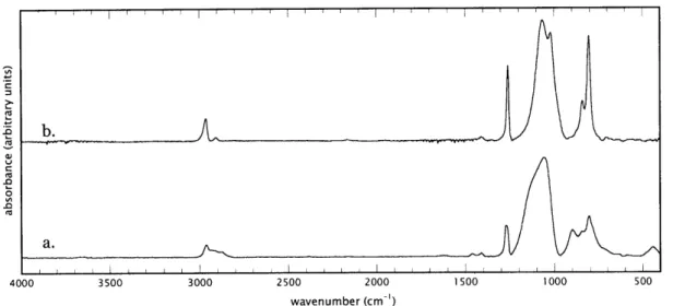
A comparison of the FTIR spectra of D3 films deposited using HFCVD and continuous-wave excitation PECVD is shown in Figures 2-2a and 2-2b. The spectrum for the CW PECVD film (Figure 2-2a) was taken from previous work by our group.3 Assignments have been made from the literature and are shown in Table 2-1. Comparison of these spectra indicates that the HFCVD film differs structurally from the PECVD film. Only sp3-carbon bonding is observed in the HFCVD film, and no crosslinking of Type II, i.e. via carbon-crosslinks, is evident.3 Carbon is thus preserved primarily as methyl, giving rise to the distinct pair of symmetric and asymmetric CH stretches23-25 at 2907 and 2964 cm-1. The asymmetric stretching
mode (ASM) of the siloxane group (SiOSi) shows two distinct bands for the HFCVD film, a characteristic observed in the IR signatures of polydimethylsiloxanes with chain lengths of more than two siloxane units or ring sizes of larger than eight units.26, 27 Below 1000 cm-l, absorption bands associated with SiMe
2 rocking and
stretching are observed at 878 and 805 cm-l, and those associated with SiMe3
rocking near 840 cm-'. Qualitatively, the PEVD film appears to have a higher SiMe3/SiMe2 ratio, suggesting that the HFCVD film may be less branched than its PECVD analog.3
. 0 3 .r (U a Iz -20 "I -0 4000 3500 3000 2500 2000 1500 1000 500 wavenumber (cm-')
Figure 2-2. FTIR spectra of a. D3 PECVD film deposited under continuous-wave
excitation and b. D3 HFCVD film deposited at ioooC.
Table 2-1. FTIR assignments from the literature.
Wavenumber (cm-) Modea Comment Reference
2963 - 2965 VAcH in sp3CH3 24, 25, 31,36 2935 VAcH in sp3CH2 24, 25 2907 VScH in sp3CH3 24, 25, 31,36 2878 VSCH in sp3CH2 24, 25 1463 8AcH2 24, 25 1412 BACH3 in SiMex 24, 25, 27,31,36 1262 8SCH3 in SiMex 25, 27, 30, 31, 36 1020 - 1075 VAsiosi 24, 25, 27, 31, 36 878 YSCH3 in SiMe2 25, 27, 30, 36
804 - 806 VAsi-c, yAcH3 in SiMe2 25, 27, 30, 31, 36
839 - 845 yAcH3 in SiMe3 25, 27, 30, 36
a, 8, and y denote stretching, bending and rocking modes respectively, A and S denote asymmetric and symmetric vibrations.
FTIR spectra of films deposited at filament temperatures of 86o0 C, 1ooo0 C, and 12000C using D3, and 8oo0 C, 9oo0C, and loooC using D4, are also shown
(Figures 2-3 and 2-4, respectively). The region around the ASM has been expanded for detail. Strong absorptions associated with SiMe2 (805 cm-'), methyl in SiMex
(1412 cm-'), and the ASM (1020-1075 cm-') are apparent. The band at about 880 cm-'
observed in the low filament temperature D4 film is usually associated with the symmetric CH3 rocking mode in SiMe2. The disappearance of this band at higher
filament temperatures may be due to the conformational constraints present in a more highly networked structure. Similar effects in this infrared region have been observed in temperature-dependent spectroscopy studies of other organosilicon compounds.2 29 'E.J C e-0 wavenumber (cm-')
Figure 2-3. FTIR spectra of D3 HFCVD films deposited at filament temperatures
of a. 86o
0C, b. ooo°C, and c. iloo°C
t) C -o I0Cd 0) -0 wavenumber (cm-')
Figure 2-4. FTIR spectra of D4 HFCVD films deposited at filament
temperatures of a. 8000C, b. 9ooC, and c. iooo°C.
Conventionally25, 27, 30, the band around 845 cm-1 is assigned to an asymmetric CH3-rocking mode in SiMe3, with an accompanying symmetric CH3-rocking mode at
760 cm-1. The SiMe3group is a chain or branch termination group that is associated
with an M group in siloxanes3, where M is the trimethylsiloxane unit (CH3)3SiO-. The
relative intensities of the SiMe2and SiMe3bands depends on the length of chains in
open-chain regions of the film structure, and the strength of the SiMe3 band is an
indication that chains are either short or highly branched.26, 31 The SiMe3/SiMe2 ratio
also increased only slightly as filament temperature was increased, suggesting that the chain length and branching was similar for both sets of films. Other data obtained for these films, particularly from NMR analysis, show only small quantities of M groups in the films, with the highest concentrations appearing in low
filament-temperature D3 and high filament-filament-temperature D4 films. This implies that short chain segments or branches of similar length are present in low concentrations in almost all the films produced.
Significant changes in the relative intensities of the bands of the ASM band are observed for both D3 and D4 films. The spectra of the D3 film shows a doublet for all three filament temperatures, with the shoulder on the doublet switching from the low- to high-wavenumber side at higher filament temperatures (compare Figures 2-3a and 2-3c). By contrast, the spectra of the D4 film deposited at a filament temperature of 800°C (Figure 2-4a) showed only a singlet, and the IR spectra resembled that of the precursor D4.2 6, 27 Unlike D4, however, which is a liquid at
room temperature, the film was solid and contiguous and came off the wafer in flakes when scraped with a razor. The D4 film deposited at higher filament temperature showed behavior similar to that of the D3 film. As filament temperature was increased, the low-wavenumber peak of the ASM doublet increased in intensity, exceeding that of the high-wavenumber peak above lo5o0C (spectra not shown), as
in the case of the D3 film.
The ASM doublet of the film deposited from D3 at a filament temperature of looC (Figure 2-3c) resembles that observed in FTIR analyses of other organosilicon PECVD films.3, 25, 32 Typically for these films, the low-wavenumber band was more intense than the high-wavenumber band. This ASM signature is also observed in spin-on methyl silsesquioxane (MSQ) films.33 For bulk polydimethylsiloxane (PDMS), the intensities of these bands are approximately equal at room temperature.34 To our knowledge, no IR spectra with an ASM doublet similar to that observed in Figures 2-3a, 2-3b and 2-4c have been reported for
organosilicon films deposited by CVD from comparable precursors. The configuration of the ASM doublet is likely to be conformational in origin. For PDMS, the splitting of the doublet has been attributed to coupling between adjacent chain
segments.31 In other work using Raman spectroscopy, the splitting of the symmetric SiOSi stretching mode has been correlated to the crystalline state of PDMS.35
The intensity ratio of the two bands of the ASM doublet has been correlated with the length of chains or size of rings in the polymethylsiloxane network.25-27 In particular, for a series of linear and cyclic polymethylsiloxanes of increasing chain length or ring size, a doublet was observed in FTIR spectra only when chain lengths exceeded two siloxane units and ring size exceeded five siloxane units. The ASM singlet for D3 was offset at 1,020 cm- 1compared to larger ring structure. The band at
1,020 cm-1 may thus be associated with an increasing proportion of six-membered D3-like rings in the film structure. This is in the same region as the low-wavenumber band of the ASM doublet in PDMS, however, making it difficult to differentiate between the presence of chains and bound D3 rings using IR analysis.3'
2.3.3 RAMAN SPECTROSCOPY
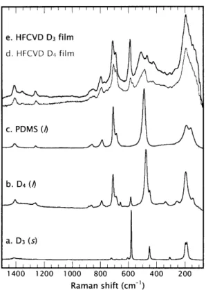
Though some work has been done in characterizing pure organosilicon compounds using Raman spectroscopy, little has been reported on the use of Raman for characterizing more complex organosilicon materials, such as those produced by CVD. Figure 2-5 compares the Raman spectra of the pure compounds D3, D4, and PDMS with that of HFCVD films grown from D3 and D4 using high filament temperatures. Assignments in Table 2-2 have been made based on the literature.28, 31,
is strong in the Raman spectra. The position of the symmetric siloxane Raman band is shifted to higher wavenumbers for D3 due to ring strain, and bands associated with ring deformation can be observed for both D3 and D4.31 Raman spectroscopy is thus a sensitive probe for observing ring structure. Indeed, Raman spectroscopy is capable of identifying siloxane ring "defects" in SiO2 films produced by sol-ge138-41
and CVD processes.42 Raman spectra for these materials exhibit specific bands corresponding to ring structures comprised of different numbers of silicon atoms. In particular, Raman bands at 605 cm-' and 495 cm-' in silica have been attributed to rings with three and four siloxane units, termed R3and R4respectively.38 39, 41 42
1400 1200 1000 800 600 400 200 Raman shift (cm-')
Figure 2-5. Micro-Raman spectra of a. D3, b. D4, c. PDMS, d. D4 HFCVD film
deposited at a filament temperature of 1ooo0 C, and e. D3 HFCVD film
Table 2-2. Raman assignments from the literature.
Raman shift (cm-l) Modea Comment Reference
1410 BACH3 23, 28, 36 1260 - 1265 8SCH3 23, 28,36 795 vAsic In SiC2 23, 28,36,37 707 - 712 VSSiC In SiC2 23, 28, 36, 37 690 YACH3 23, 28,37 581 VSsiosi In D3 31,37,72 489 VSsiosi In PDMS 23, 36
476 vssiosi and/or ring deformation In D4 23, 37
450 Ring deformation In D3 and D4 23, 37
424 - 426 Possible Si-Si stretch 44
190 - 194 §Ssic in SiC2 31,37
160 §Ssic and twist In PDMS 31
145 8Ssic In D4 31
av, 6 and y, denote stretching, bending and rocking modes respectively, A and A denote asymmetric and symmetric vibrations.
As observed in Figure 2-5, the Raman shift region of the HFCVD films from 400 cm-' to 60o cm-l differs from that of the pure compounds. Both HFCVD films show a band in the range 586 - 590 cm-l which is not observed in PDMS or other linear siloxane compounds.3' This is close to the band assigned to the siloxane symmetric stretching mode (SSM) at 581 cm-l in pure D3. During an experiment in which polarization of the Raman beam was changed from the parallel to the perpendicular mode, the band in the HFCVD film was also found to be polarized, which is consistent with results observed for the SSM in D3. 3, 37 This band may thus be evidence of a bound D3-like ring structure in the film. The 5 - lo cm-' shift from the position of this band in D3 may be conformational in origin and a result of the strain of being locked into a semi-networked structure. Such shifts are possible, and Table 2-3 shows Raman assignments for the SSM mode in different chemical
environments. In the highly networked environment of vitreous and chemical vapor-deposited silica, the characteristic vibrational mode of the six-membered planar ring of siloxane units,
R
3, has been observed at shifts as high as6o8
cm-.38, 40, 43 By contrast, the SSM mode is typically observed from 581-587 cm-' for unconstrained D3. The band around 590 cm-' for the HFCVD films falls between these extremes, and is thus assigned to an oR3 group. The term oRn is derived from theRn
unitobserved in silica, and is intended to represent an organically substituted ring consisting of n siloxane units, which is bound into the film structure. By analogy, there may also be rings consisting of four siloxane units bound into the film structure
(oR4). Table 2-3 shows that the band at 485 cm-' observed primarily for the D4
HFCVD films falls between the SSM bands for D in PDMS, R4 in silica, and
unperturbed D4. This suggests that the band is associated with oR4 groups and/or
unstrained siloxane units in the film. The unstrained siloxane units may be present in linear structures or in ring structures larger than four units, and are designated as
ID. The predominance of these groups in the D4 films, particularly at low filament
temperature, suggest that they are unique to the pyrolysis chemistry of D4 and may be the four siloxane-unit ring analog, oR4.
Table 2-3. Raman siloxane symmetric stretching mode (SSM) assignments
Symbol Raman shift (cm-l) Comment Reference
R3 600-608 In vitreous and/or CVD silica. 38-42 oR3 586-590 In D3 and D4 HFCVD films.
D3 581-587 In D3. 31,37, 72
D 489-497 In PDMS. 23,36
R4 490-495 In vitreous and/or CVD silica. 38-42
oR4 and/or ID 485 In D3 and D4 HFCVD films.
D4 475-480 In D4. 23,28,36,37
The Raman spectra of the HFCVD films also show a low-intensity band at 425 cm-' not observed in any of the pure compounds. No assignment could be found for this band in the literature, but it is in the region associated with a silicon-silicon stretching mode.44 The Si-Si stretch gives a strong Raman band at 400 - 405 cm-l for hexamethyldisilane, and is highly sensitive to silicon substituents. For polar substituents, shifts can be large. For example, the Si-Si stretching mode for FMe2SiSiMe2F has been reported at 433 cm-', a shift of 30 cm-' from the
unsubstituted disilane.45 Hence, this band is tentatively assigned to a Si-Si bond in the film structure.
900 800 700 600 500 400 300 200 100 Raman shift (cm- ')
Figure 2-6. Micro-Raman spectra of D3 HFCVD films deposited at filament
temperatures of 86o0 C, 1ooo0 C, and 110oo0 C.
900 800 700 600 500 400 300 200 Raman shift (cm- ')
1 00
Figure 2-7. Micro-Raman spectra of D4 HFCVD films deposited at filament
Figure 2-6 and 2-7 show the effect of filament temperature as probed by Raman spectroscopy. The spectra of the films deposited from D3 (Figure 2-6) show an increasing intensity of the bands from oR3 units and Si-Si bonds as filament
temperature is increased, and the D3 film deposited at n1oo0 C shows significant ring incorporation. FTIR spectra for these films show a similar increase in intensity in the low-wavenumber band of the ASM doublet (see Figure 2-3), suggesting that this band at 1020 cm-' is indeed associated with three siloxane-unit ring structures. By
contrast, the spectra of the films deposited from D4 (Figure 2-7) show a strong band at 485 cm-', assigned to the presence of oR4 and/or unstrained D units. A slight
increase in oR3 incorporation is observed as Tf increases, but this band does not
dominate as it does in the spectra of the D3 films (Figure 2-6). Hence, the D3 and D4 films differ structurally at high filament temperatures, despite the similarities in structures suggested by FTIR.
2.3.4 NUCLEAR MAGNETIC RESONANCE (NMR) SPECTROSCOPY
The 29Si CP-MAS NMR spectra obtained for the D3 and D4 HFCVD films are
shown in Figures 2-8 and 2-9. Typical chemical shifts reported in the literature for organosilicon CVD films are included in Table 2-4.20, 32, 46-49 As suggested by the data in this table, films deposited by other CVD methods commonly show a wide variety of bonding environments, including the presence of M, D, T, and Q groups as well as their hydrogenated analogs.32, 49, 50 By contrast, only two primary peaks were observed in these HFCVD films.