HAL Id: hal-02920129
https://hal.archives-ouvertes.fr/hal-02920129
Submitted on 7 Nov 2020
HAL is a multi-disciplinary open access
archive for the deposit and dissemination of
sci-entific research documents, whether they are
pub-lished or not. The documents may come from
teaching and research institutions in France or
abroad, or from public or private research centers.
L’archive ouverte pluridisciplinaire HAL, est
destinée au dépôt et à la diffusion de documents
scientifiques de niveau recherche, publiés ou non,
émanant des établissements d’enseignement et de
recherche français ou étrangers, des laboratoires
publics ou privés.
Architecture for SiC MOSFETs
Nicolas Rouger, Yazan Barazi, Marc Cousineau, Frédéric Richardeau
To cite this version:
Nicolas Rouger, Yazan Barazi, Marc Cousineau, Frédéric Richardeau.
Modular Multilevel
SOI-CMOS Active Gate Driver Architecture for SiC MOSFETs. 2020 32nd International Symposium
on Power Semiconductor Devices and ICs (ISPSD), Sep 2020, Vienna (virtual ), Austria. pp.278-281,
�10.1109/ISPSD46842.2020.9170181�. �hal-02920129�
Modular Multilevel SOI-CMOS Active Gate Driver
Architecture for SiC MOSFETs
Nicolas Rouger, Yazan Barazi, Marc Cousineau, Fréderic Richardeau
LAPLACE, Université de Toulouse, CNRS, INPT, UPS, Toulouse, France 2 rue Charles Camichel Toulouse, BP7122 – 31071 Toulouse Cedex 07, FranceAbstract— High Voltage SiC power MOSFETs have specific driving challenges such as a reduced short circuit capability (compared
to Si IGBTs) and a weak field oxide layer, a large gate to source driving voltage (compared to GaN FETs), a high electric field under negative gate bias in off-state and a high switching speed. The negative bias in off-state creates a high stress which reduces the reliability of the SiC MOSFET. The high positive gate bias can generate large drain saturation current in case of short circuit events. We propose a modular multilevel architecture, which takes benefits of SOI isolation and low voltage CMOS transistors to drive SiC MOSFETs and to improve their reliability using an active and dynamic multilevel-selection on the switching sequences and on/off states.
Keywords—active gate driver; multi-level; SiC gate drivers; SOI CMOS.
I. INTRODUCTION
Wide bandgap power transistors such as SiC MOSFETs show improvements on the efficiency – power density trade-off for next generation power converters. However, SiC MOSFETs have specific behaviors which impact performances, reliability and their dedicated gate drivers: the drain current is governed by majority carriers and channel characteristics [1-3], the gate to source voltage swing is rather large to achieve a low on state resistance (high positive VGS, e.g. +18V or +20V) and to guarantee a
sufficient immunity to higher dVDS/dt and Miller parasitic coupling (negative VGS, e.g. -4V). To improve the overall performances
and reliability of SiC MOSFETs and to offer new gate driving degrees of freedom, we propose an original multilevel gate driver architecture (building-block approach) on a single CMOS IC. The principle is to use the highly efficient low voltage 5V transistors and capacitors for the gate driver, and to connect several stages in series, each stage being isolated via Deep Trench Isolation (DTI) and integrated on the same chip. As a consequence, the applied gate-to-source voltage of the SiC power MOSFET can be easily shaped, with new functionalities.
II. CLASSICAL TOPOLOGY
Typically, the output buffer stage of gate drivers for SiC MOSFETs is based on a split output current amplification push-pull (Fig. 1,2). However, this simple circuit suffers from important limitations: a) the SiC gate driving voltages are linked with the IC technology and gate driver supply levels, hence neither their values nor the switching speed can be dynamically and quickly tuned. High voltage CMOS MOSFETs (e.g. >40V) are required to be compatible with SiC driving voltages. b) Under hard switching fault (HSF) type I short-circuit, the SiC MOSFET’s drain current is only limited by the high saturation current (between 7 and 10 times the rated current), which is related to the large applied gate-to-source voltage during turn-on and the low VGSth compared to Si
MOSFETs (Fig. 3). c) to increase the safety margin of parasitic Miller coupling during dVDS/dt, the negative VGS during off-state
charge is dissipated through the RGoff gate resistor during turn-off, whereas recycling such a gate charge would offer the possibility
to downsize the isolated gate power supply. As a consequence of these limitations, one would like to actively tune the gate to source driving voltage of SiC MOSFETs, to combine a high switching speed capability, low on-state resistance, high immunity to dVDS/dt, improved short circuit capability, and to modify the gate driver architecture.
III. PROPOSED ARCHITECTECTURE
A. Modular Multilevel Active Gate Driver
PWM Vgs Igs tp=10ns tr=30ns Ipeak=1.55 A RgON=RgOFF=10 Ω Ciss= 1nF 0V +4.5V -4V
Generates large SiC saturation currents in case of HSF +16V
-4V Generates high
Electric Field, SiC gate oxide stress
50ns
Fig. 2. Simulated waveforms of Fig. 1, with a constant Ciss (1nF). Two key challenges are highlighted in red, with a typical +16V/-4V VGS driving.
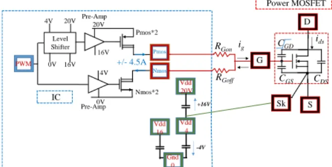
ids ig CGD CGS CDS 20V 16V Level Shifter 20V 16V 4V 0V Pmos*2 Pre-Amp 4V 0V Nmos*2 Pre-Amp RGon RGoff PWM Pmos Nmos +/- 4.5A S G D Sk IC Vdd 16 Gnd 0 Vdd 20V Vdd 4 +16V -4V Power MOSFET
Fig. 1. Classical CMOS push-pull buffer with split output, driving SiC MOSFET with Kelvin Source.
Vgs=+23V .. +18V Step 1V
Ids Vds
Fig. 3. Experimental Short-Circuit behavior of a 80mOhm - 1.2kV SiC MOSFET at 600V. Left, the measured dependence of the saturation IDS
To offer an improved driving scheme for SiC MOSFETs, we propose a Modular Multilevel Active Gate Driver (MMAGD). Other attempts for multilevel gate drivers have been presented in the literature, mainly with discrete solutions [4-10], while active gate drivers focused on improved switching loss – EMI tradeoff [11,12] or short circuit protection [13]. The core idea here is to cascade 5V CMOS push-pull circuits in series, each being supplied by the energy stored in 5V floating capacitors (Fig 4.). This technique can also be applied with 1.8V or other voltages, which takes benefits of low voltage transistors and integrated capacitors with better figures of merit than high voltage CMOS transistors (e.g. >40V) for 2-level gate drivers. However, it is required to isolate each low voltage transistor, due to the non-zero common mode voltage (e.g. higher than 20V) and floating potentials as a function of the state of the other series-connected transistors. As a consequence, the XFAB XT018 SOI CMOS technology (180nm) was chosen, thanks to its isolation capability with DTI, efficient 1.8V digital, 5V-40V analog CMOS, high density passive
components, high temperature capability and its availability through MPW. Each floating push-pull, pre-amplification circuits and
level shifters are identical and can be described as an elementary 5V submodule, which must be compatible with the specified common mode voltages. As presented in Fig 4., we propose to monolithically integrate five identical submodules (four towards the gate, one to the Kelvin source) to allow a 6-level driving possibility, and both positive and negative VGS. There is no modification
on the SiC MOSFET and its interconnection with the gate driver, as highlighted by the IC boundary in Fig 1. and Fig 4. Fig 5. shows the simulation of the MMAGD, where each floating capacitor is previously charged at 4V and an improved SiC driving is proposed. The PWM0..4 signals are generated based on the input PWM signal and the desired SiC VGS voltage sequence. Several
voltage levels can also be obtained by a different combination of PWM0..4 signals (e.g. VGS =0V, +4V..+12V). Benefits of the
MMAGD are highlighted in Fig 5: a reduced HSF short circuit current thanks to a reduced VGS only during turn-on (albeit higher
than the worst case Miller plateau voltage), a high VGS for low SiC conduction losses, a dynamic negative VGS to improve immunity
to dVDS/dt (high/low side crosstalk), and a zero VGS in off-state to reduce the SiC field oxide stress [1-2]. Even if the VGS voltage is
reduced to +12V during turn-on, the peak gate current is maintained high to guarantee high switching speeds and low SiC switching losses thanks to a lower gate resistance than the one in classical 2-level operation. One has to note that the source internal resistance distributed on each submodule naturally contributes to this apparent gate resistance. The floating capacitors can be recharged by two ways: each submodule has a bootstrap-like circuit which can recharge its floating capacitor as long as the floating ground GND_HV0..4 is connected to the IC GND, and/or by harvesting a part of the SiC gate charge during switching transitions.
B. Preliminary results
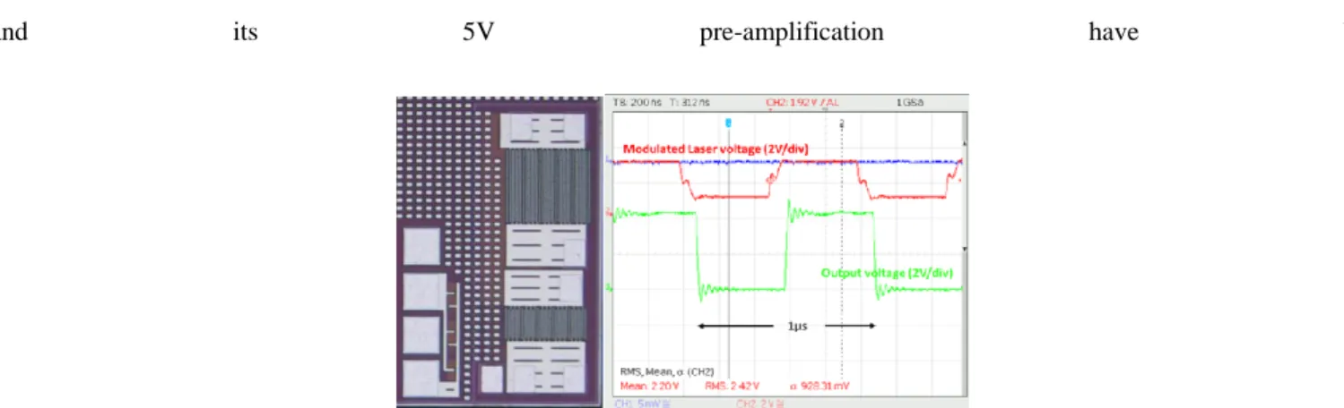
Fig. 7. presents the characterization of one 5V submodule, which was designed and previously validated [14]. The output 5V PMOS and NMOS of one submodule have a RDSon of 0.26Ω (25°C), +/- 5A source/sink capability and a maximum slew rate of
5V/ns. Other specifications can be found in [14].
C. Design and layout of the SOI-CMOS MMAGD
Each submodule is based on the previously proposed 5V-0.26Ω split output buffer. Hence the complete MMAGD exhibits a maximal total gate driver resistance of 1.3Ω for 5 submodules connected in series. In each submodule, the 5V split output buffer
Level 1: Vgs=0V
static turn-off at low field stress for DUT'SiO2
and improved 3rq quadrant operation (static and dynamic)
Level 2: Vgs=+12V
dynamic turn-on with low drain – source saturation current enabling a safe operation and a non critical protection delay in short-circuit event
Level 1 Vgs=0V Level 3 Vgs=+16V Level 2 Vgs=+12V Level 4 Vgs=-4V 2µs
Level 3: Vgs=+16V
static on-state at high gate – source bias with low drop voltage and low on-state losses
Level 4: Vgs=-4V
dynamic turn-off
with high cross-talk immunity
Fig. 5. VGS simulated waveform with the multilevel architecture from Fig.4., highlighting the benefits of the proposed multilevel driving scheme on the SiC
and its 5V pre-amplification have been
within DTI-isolated P-type substrates. To be able to send the PWM0..4 activation signals from an input signal referenced to the IC global GND (labeled Gnd! on Fig 4.), differential level shifters are also integrated in each submodule. The level shifters are based on 40V-class CMOS transistors and optimized to reduce propagation delays and consumption. The comparison of turn-on and turn-off for a grounded or floating submodule is presented in fig.8. To store enough energy and to generate 4V floating supplies for each submodule, 180pF double density 5V-class MIM capacitors are integrated on chip. It is however possible to extend the stored energy through external capacitors, however it is then required to add extra bonding wires to further connect to external capacitors for Gnd_HV2..4 and Vdd_HV2..4. This tradeoff between floating capacitor integration and constraints on packaging will be further optimized. In order to recharge the 4V floating capacitors for each submodule, a low voltage drop bootstrap circuit is integrated. This bootstrap consists of a current source associated with a high voltage transistor rated for a maximum current of 0.1A and blocking capability of more than 40V. First, an enable signal, En_LV0..4, referenced to the chip ground Gnd!, activates the charge transfer from the global 4V Vdd_LV to the floating submodule, should its floating ground Gnd_HV0..4 be connected to the IC ground Gnd!. As soon as the floating Vdd_HV0..4 has a high enough value, the low drop bootstrap can be activated through En_HV0..4, reducing to less than 1mV the total bootstrap voltage drop to guarantees that Vdd_HV0..4 reaches Vdd_LV (e.g. 4V). These floating capacitors can also be recharged by recycling the stored SiC gate charge, if the PWM0..4 states offer a path for the gate current to flow through the floating capacitors. A protection diode is also integrated to prevent over voltages. Fig 4. and 5. show the fabricated IC, which has been packaged in QFN40 6mmx6mm. The ongoing experimental validations are aiming to compare the fabricated monolithic CMOS MMAGD with a PCB-integration of five submodules, and to demonstrate the driving and reliability improvements on SiC MOSFETs.
IV. CONCLUSION
An innovative architecture for an active gate driver for SiC MOSFET has been proposed, simulated and designed. This modular multilevel active gate driver (MMAGD) offers new perspectives to tune the voltage levels of power MOSFETs during their switching transients. The key benefits of the MMAGD are to use elementary low differential voltage submodules, to reduce the stress for SiC short-circuit detection and protection, to reduce the electric field on the SiC gate stack during on-state while keeping a high immunity to Miller coupling, to offer the recharge of the integrated floating capacitors on each submodule and to reduce the isolated gate driver supply to 5V rather than 16-20V. In our first prototype, large values of floating capacitors are integrated on-chip to be able to assess the possibility to remove any external floating capacitor to supply the floating submodules. Experimental characterization of the monolithic MMAGD on SOI-CMOS is ongoing, with a focus on the optimized control technique to actively drive SiC MOSFETs and to recharge the floating capacitors with the highest efficiency. The benefits of the modified gate driving scheme are also under investigation by further experimentations.
5V Capacitor – 180pF 5V PMOS 5V NMOS 5V preamp Low drop Bootstrap 6V protection diode Vdd HV1 GND HV1
Fig. 9. Optical microscope picture of one submodule (Zoom of fig 4. on the submodule 1). Area is 1050µm x 500µm.
Fig. 8. Simulations of one 5V submodule from Fig. 4. a) Input and output waveforms for different voltage supply values (submodule floating ground at 0V). b) Input and output waveforms at 4V, with the submodule floating ground at 12V (Rg at 0 or 10 ohms).
ACKNOWLEDGMENT
The authors thank Dr. F. Boige and Ing. J.M Blaquiere (Laplace) for the short circuit test bench, Dr. L.T. Le, Dr. JC. Crébier (G2Elab) for the preliminary experimental results of the 5V buffer. We thank Europractice-IC and IMEC for MPW and technical support, as well as XFAB for fruitful discussions and technical exchanges.
REFERENCES
[1] T. Hosoi et al., "Reliability-aware design of metal/high-k gate stack for high-performance SiC power MOSFET," 2017 29th (ISPSD), Sapporo, 2017, pp. 247-250.
[2] S. Wirths et al., "Vertical 1.2kV SiC Power MOSFETs with High-k/Metal Gate Stack," 2019 31st (ISPSD), Shanghai, China, 2019, pp. 103-106.
[3] A Fayyaz, F. Boige, A Borghese, G Guibaud, V. Chazal, et al. “Aging and failure mechanisms of SiC Power MOSFETs under repetitive short- circuit pulses of different duration”, ICSCRM 2019, Japan
[4] S. Zhao et al., "Adaptive Multi-Level Active Gate Drivers for SiC Power Devices," in IEEE Transactions on Power Electronics, vol. 35, no. 2, pp. 1882-1898, Feb. 2020.
[5] R. Ning, Y. Zhou, A. Kundu and Z. J. Shen, "Feasibility and Limitation of DC/DC Multilevel Converter Power ICs Using Standard CMOS Transistors," 2019 31st (ISPSD), Shanghai, China, 2019, pp. 107-110.
[6] Z. Dong, Z. Zhang, X. Ren, X. Ruan and Y. Liu, "A gate drive circuit with mid-level voltage for GaN transistors in a 7-MHz isolated resonant converter," 2015 IEEE Applied Power Electronics Conference and Exposition (APEC), Charlotte, NC, 2015, pp. 731-736.
[7] H. C. P. Dymond, D. Liu, J. Wang, J. J. O. Dalton and B. H. Stark, "Multi-level active gate driver for SiC MOSFETs," 2017 IEEE Energy Conversion Congress and Exposition (ECCE), Cincinnati, OH, 2017, pp. 5107-5112.
[8] A. Dearien, S. Zhao, C. Farnell and H. A. Mantooth, "Slew Rate Control of High-Voltage SiC MOSFETs using Gate Resistance vs. Intermediate Voltage Level," 2019 10th International Conference on Power Electronics and ECCE Asia (ICPE 2019 - ECCE Asia), Busan, Korea (South), 2019, pp. 2146-2152. [9] Z. Zeng and X. Li, "Comparative Study on Multiple Degrees of Freedom of Gate Drivers for Transient Behavior Regulation of SiC MOSFET," in IEEE
Transactions on Power Electronics, vol. 33, no. 10, pp. 8754-8763, Oct. 2018.
[10] N. Idir, R. Bausiere and J. J. Franchaud, "Active gate voltage control of turn-on di/dt and turn-off dv/dt in insulated gate transistors," in IEEE Transactions on Power Electronics, vol. 21, no. 4, pp. 849-855, July 2006.
[11] P. Bau et al., "Sub-Nanosecond Delay CMOS Active Gate Driver for Closed-Loop dV/dt Control of GaN Transistors," 2019 31st International Symposium on Power Semiconductor Devices and ICs (ISPSD), Shanghai, China, 2019, pp. 75-78.
[12] J. Chen et al., “A Smart IGBT Gate Driver IC with Temperature Compensated Collector Current Sensing”, in IEEE Transactions on Power Electronics, vol. 34, no. 5, pp. 4613-4627, May 2019.
[13] D. Sadik et al., “Short-Circuit Protection Circuits for Silicon-Carbide Power Transistors”, in IEEE Transactions on Industrial Electronics, vol. 63, no. 4, pp. 1995-2004, April 2016.
[14] N. Rouger, L. T. Le, D. Colin and J. Crébier, "CMOS SOI gate driver with integrated optical supply and optical driving for fast power transistors," 2016 28th ICs (ISPSD), Prague, 2016, pp. 427-430.
![Fig. 7. presents the characterization of one 5V submodule, which was designed and previously validated [14]](https://thumb-eu.123doks.com/thumbv2/123doknet/14360445.502523/5.893.150.758.204.378/fig-presents-characterization-v-submodule-designed-previously-validated.webp)